EP1197943A2 - Driving circuit for an organic electroluminescent element, electronic equipment, and electro-optical device - Google Patents
Driving circuit for an organic electroluminescent element, electronic equipment, and electro-optical device Download PDFInfo
- Publication number
- EP1197943A2 EP1197943A2 EP01308730A EP01308730A EP1197943A2 EP 1197943 A2 EP1197943 A2 EP 1197943A2 EP 01308730 A EP01308730 A EP 01308730A EP 01308730 A EP01308730 A EP 01308730A EP 1197943 A2 EP1197943 A2 EP 1197943A2
- Authority
- EP
- European Patent Office
- Prior art keywords
- reverse
- electro
- organic electroluminescent
- driving circuit
- switch
- Prior art date
- Legal status (The legal status is an assumption and is not a legal conclusion. Google has not performed a legal analysis and makes no representation as to the accuracy of the status listed.)
- Granted
Links
- 239000011159 matrix material Substances 0.000 claims description 34
- 230000002035 prolonged effect Effects 0.000 abstract description 6
- 238000010586 diagram Methods 0.000 description 17
- 230000003071 parasitic effect Effects 0.000 description 15
- 238000010276 construction Methods 0.000 description 12
- 239000010410 layer Substances 0.000 description 12
- 239000012212 insulator Substances 0.000 description 11
- 230000004044 response Effects 0.000 description 7
- 239000010409 thin film Substances 0.000 description 7
- 239000011229 interlayer Substances 0.000 description 6
- 229910052751 metal Inorganic materials 0.000 description 5
- 239000002184 metal Substances 0.000 description 5
- 238000000034 method Methods 0.000 description 5
- 239000000463 material Substances 0.000 description 4
- 230000003287 optical effect Effects 0.000 description 3
- 230000015556 catabolic process Effects 0.000 description 2
- 238000006731 degradation reaction Methods 0.000 description 2
- 239000010408 film Substances 0.000 description 2
- 230000006870 function Effects 0.000 description 2
- 239000004065 semiconductor Substances 0.000 description 2
- 229920001621 AMOLED Polymers 0.000 description 1
- 241001076195 Lampsilis ovata Species 0.000 description 1
- 108010075750 P-Type Calcium Channels Proteins 0.000 description 1
- 239000003990 capacitor Substances 0.000 description 1
- 239000003086 colorant Substances 0.000 description 1
- 239000004020 conductor Substances 0.000 description 1
- 230000005684 electric field Effects 0.000 description 1
- 238000001962 electrophoresis Methods 0.000 description 1
- 239000011521 glass Substances 0.000 description 1
- AMGQUBHHOARCQH-UHFFFAOYSA-N indium;oxotin Chemical compound [In].[Sn]=O AMGQUBHHOARCQH-UHFFFAOYSA-N 0.000 description 1
- 238000002347 injection Methods 0.000 description 1
- 239000007924 injection Substances 0.000 description 1
- 239000004973 liquid crystal related substance Substances 0.000 description 1
- 238000012544 monitoring process Methods 0.000 description 1
- 238000000926 separation method Methods 0.000 description 1
- 239000000758 substrate Substances 0.000 description 1
- 230000001052 transient effect Effects 0.000 description 1
Images


Classifications
-
- G—PHYSICS
- G09—EDUCATION; CRYPTOGRAPHY; DISPLAY; ADVERTISING; SEALS
- G09G—ARRANGEMENTS OR CIRCUITS FOR CONTROL OF INDICATING DEVICES USING STATIC MEANS TO PRESENT VARIABLE INFORMATION
- G09G3/00—Control arrangements or circuits, of interest only in connection with visual indicators other than cathode-ray tubes
- G09G3/20—Control arrangements or circuits, of interest only in connection with visual indicators other than cathode-ray tubes for presentation of an assembly of a number of characters, e.g. a page, by composing the assembly by combination of individual elements arranged in a matrix no fixed position being assigned to or needed to be assigned to the individual characters or partial characters
- G09G3/22—Control arrangements or circuits, of interest only in connection with visual indicators other than cathode-ray tubes for presentation of an assembly of a number of characters, e.g. a page, by composing the assembly by combination of individual elements arranged in a matrix no fixed position being assigned to or needed to be assigned to the individual characters or partial characters using controlled light sources
- G09G3/30—Control arrangements or circuits, of interest only in connection with visual indicators other than cathode-ray tubes for presentation of an assembly of a number of characters, e.g. a page, by composing the assembly by combination of individual elements arranged in a matrix no fixed position being assigned to or needed to be assigned to the individual characters or partial characters using controlled light sources using electroluminescent panels
- G09G3/32—Control arrangements or circuits, of interest only in connection with visual indicators other than cathode-ray tubes for presentation of an assembly of a number of characters, e.g. a page, by composing the assembly by combination of individual elements arranged in a matrix no fixed position being assigned to or needed to be assigned to the individual characters or partial characters using controlled light sources using electroluminescent panels semiconductive, e.g. using light-emitting diodes [LED]
- G09G3/3208—Control arrangements or circuits, of interest only in connection with visual indicators other than cathode-ray tubes for presentation of an assembly of a number of characters, e.g. a page, by composing the assembly by combination of individual elements arranged in a matrix no fixed position being assigned to or needed to be assigned to the individual characters or partial characters using controlled light sources using electroluminescent panels semiconductive, e.g. using light-emitting diodes [LED] organic, e.g. using organic light-emitting diodes [OLED]
- G09G3/3225—Control arrangements or circuits, of interest only in connection with visual indicators other than cathode-ray tubes for presentation of an assembly of a number of characters, e.g. a page, by composing the assembly by combination of individual elements arranged in a matrix no fixed position being assigned to or needed to be assigned to the individual characters or partial characters using controlled light sources using electroluminescent panels semiconductive, e.g. using light-emitting diodes [LED] organic, e.g. using organic light-emitting diodes [OLED] using an active matrix
- G09G3/3233—Control arrangements or circuits, of interest only in connection with visual indicators other than cathode-ray tubes for presentation of an assembly of a number of characters, e.g. a page, by composing the assembly by combination of individual elements arranged in a matrix no fixed position being assigned to or needed to be assigned to the individual characters or partial characters using controlled light sources using electroluminescent panels semiconductive, e.g. using light-emitting diodes [LED] organic, e.g. using organic light-emitting diodes [OLED] using an active matrix with pixel circuitry controlling the current through the light-emitting element
- G09G3/3241—Control arrangements or circuits, of interest only in connection with visual indicators other than cathode-ray tubes for presentation of an assembly of a number of characters, e.g. a page, by composing the assembly by combination of individual elements arranged in a matrix no fixed position being assigned to or needed to be assigned to the individual characters or partial characters using controlled light sources using electroluminescent panels semiconductive, e.g. using light-emitting diodes [LED] organic, e.g. using organic light-emitting diodes [OLED] using an active matrix with pixel circuitry controlling the current through the light-emitting element the current through the light-emitting element being set using a data current provided by the data driver, e.g. by using a two-transistor current mirror
- G09G3/325—Control arrangements or circuits, of interest only in connection with visual indicators other than cathode-ray tubes for presentation of an assembly of a number of characters, e.g. a page, by composing the assembly by combination of individual elements arranged in a matrix no fixed position being assigned to or needed to be assigned to the individual characters or partial characters using controlled light sources using electroluminescent panels semiconductive, e.g. using light-emitting diodes [LED] organic, e.g. using organic light-emitting diodes [OLED] using an active matrix with pixel circuitry controlling the current through the light-emitting element the current through the light-emitting element being set using a data current provided by the data driver, e.g. by using a two-transistor current mirror the data current flowing through the driving transistor during a setting phase, e.g. by using a switch for connecting the driving transistor to the data driver
-
- G—PHYSICS
- G09—EDUCATION; CRYPTOGRAPHY; DISPLAY; ADVERTISING; SEALS
- G09G—ARRANGEMENTS OR CIRCUITS FOR CONTROL OF INDICATING DEVICES USING STATIC MEANS TO PRESENT VARIABLE INFORMATION
- G09G2300/00—Aspects of the constitution of display devices
- G09G2300/08—Active matrix structure, i.e. with use of active elements, inclusive of non-linear two terminal elements, in the pixels together with light emitting or modulating elements
- G09G2300/0809—Several active elements per pixel in active matrix panels
- G09G2300/0819—Several active elements per pixel in active matrix panels used for counteracting undesired variations, e.g. feedback or autozeroing
-
- G—PHYSICS
- G09—EDUCATION; CRYPTOGRAPHY; DISPLAY; ADVERTISING; SEALS
- G09G—ARRANGEMENTS OR CIRCUITS FOR CONTROL OF INDICATING DEVICES USING STATIC MEANS TO PRESENT VARIABLE INFORMATION
- G09G2300/00—Aspects of the constitution of display devices
- G09G2300/08—Active matrix structure, i.e. with use of active elements, inclusive of non-linear two terminal elements, in the pixels together with light emitting or modulating elements
- G09G2300/0809—Several active elements per pixel in active matrix panels
- G09G2300/0842—Several active elements per pixel in active matrix panels forming a memory circuit, e.g. a dynamic memory with one capacitor
- G09G2300/0861—Several active elements per pixel in active matrix panels forming a memory circuit, e.g. a dynamic memory with one capacitor with additional control of the display period without amending the charge stored in a pixel memory, e.g. by means of additional select electrodes
- G09G2300/0866—Several active elements per pixel in active matrix panels forming a memory circuit, e.g. a dynamic memory with one capacitor with additional control of the display period without amending the charge stored in a pixel memory, e.g. by means of additional select electrodes by means of changes in the pixel supply voltage
-
- G—PHYSICS
- G09—EDUCATION; CRYPTOGRAPHY; DISPLAY; ADVERTISING; SEALS
- G09G—ARRANGEMENTS OR CIRCUITS FOR CONTROL OF INDICATING DEVICES USING STATIC MEANS TO PRESENT VARIABLE INFORMATION
- G09G2310/00—Command of the display device
- G09G2310/02—Addressing, scanning or driving the display screen or processing steps related thereto
- G09G2310/0243—Details of the generation of driving signals
- G09G2310/0251—Precharge or discharge of pixel before applying new pixel voltage
-
- G—PHYSICS
- G09—EDUCATION; CRYPTOGRAPHY; DISPLAY; ADVERTISING; SEALS
- G09G—ARRANGEMENTS OR CIRCUITS FOR CONTROL OF INDICATING DEVICES USING STATIC MEANS TO PRESENT VARIABLE INFORMATION
- G09G2310/00—Command of the display device
- G09G2310/02—Addressing, scanning or driving the display screen or processing steps related thereto
- G09G2310/0243—Details of the generation of driving signals
- G09G2310/0254—Control of polarity reversal in general, other than for liquid crystal displays
- G09G2310/0256—Control of polarity reversal in general, other than for liquid crystal displays with the purpose of reversing the voltage across a light emitting or modulating element within a pixel
-
- G—PHYSICS
- G09—EDUCATION; CRYPTOGRAPHY; DISPLAY; ADVERTISING; SEALS
- G09G—ARRANGEMENTS OR CIRCUITS FOR CONTROL OF INDICATING DEVICES USING STATIC MEANS TO PRESENT VARIABLE INFORMATION
- G09G2320/00—Control of display operating conditions
- G09G2320/04—Maintaining the quality of display appearance
- G09G2320/043—Preventing or counteracting the effects of ageing
-
- H—ELECTRICITY
- H10—SEMICONDUCTOR DEVICES; ELECTRIC SOLID-STATE DEVICES NOT OTHERWISE PROVIDED FOR
- H10K—ORGANIC ELECTRIC SOLID-STATE DEVICES
- H10K59/00—Integrated devices, or assemblies of multiple devices, comprising at least one organic light-emitting element covered by group H10K50/00
- H10K59/10—OLED displays
- H10K59/12—Active-matrix OLED [AMOLED] displays
Definitions
- the present invention relates to a driving circuit for driving an active-matrix display device employing organic electroluminescent elements, and electronic equipment and an electro-optical device, incorporating the driving circuit, and, more particularly, to a driving circuit having the function of applying a reverse-bias voltage to an organic electroluminescent element for controlling degradation of the organic electroluminescent element, and electronic equipment and an electro-optical device, incorporating the driving circuit.
- an organic EL display device is produced by arranging a plurality of pixels of organic electroluminescent elements, i.e., one of electro-optical elements, in a matrix.
- the organic electroluminescent element includes a metal electrode of Mg:Ag or A1:Li, etc., as a cathode, a transparent electrode such as an ITO (Indium Tin Oxide) as an anode, and an organic thin-film laminate, including an emission layer, interposed between the cathode and the anode.
- FIG. 9 shows a typical construction of a driving circuit for an active matrix display device employing an organic electroluminescent element.
- the organic electroluminescent element is shown as a diode 10.
- the driving circuit is composed of transistors Tr 1 and Tr 2, each constructed of a thin-film transistor (TFT), and a capacitive element 2 storing charge.
- TFT thin-film transistor
- Both the transistor Tr 1 and the transistor Tr 2 are of a p-channel TFT.
- the conduction state of the transistor Tr 1 is controlled in response to a charge stored in the capacitive element 2 as shown.
- the capacitive element 2 is charged through a data line V DATA by the transistor Tr 2, which is turned on with a selection voltage V SEL driven low.
- V DATA data line
- V SEL selection voltage
- FIG. 10 shows a simple timing diagram for the circuit shown in FIG. 9.
- the selection voltage V SEL is driven low as shown FIG. 10.
- the transistor Tr 2 is turned on, thus charging the capacitive element 2.
- the charge duration is a write period T W .
- An actual presentation period follows the write period T W .
- charge stored in the capacitive element 2 controls the conduction state of the transistor Tr 1.
- the presentation period is represented by T H as shown.
- FIG. 11 shows another arrangement of the organic electroluminescent element driving circuit.
- the driving circuit shown is described in a paper entitled “The Impact of Transient Response of Organic Light Emitting Diodes on the Design of Active Matrix OLED Displays” (1998 IEEE IEDM98-875).
- a driving transistor Tr 1 a charge control transistor Tr 2
- a first selection transistor Tr 3 a first selection transistor Tr 3
- a second selection transistor Tr 4 which is turned off during a charging period of the capacitive element 2.
- transistors even complying with the same specifications, suffer variations in performance. Even when the same voltage is applied to the gates of transistors, these transistor do not necessarily permit current of equal values to flow therethrough. Such variations cause nonuniformity in brightness.
- a current source 4 feeds a write current corresponding to a data signal, and the data signal thus controls the gate voltage of the transistor. In this way, the emission state of the organic electroluminescent element is controlled.
- Transistors Tr 1 through Tr 4 are all of a p-type channel transistor.
- the selection voltage V SEL is driven low, the transistors Tr 2 and Tr 3 are turned on, thereby storing in the capacitive element 2 a charge corresponding to the value of the output of the current source 4.
- the selection voltage V SEL is driven high, the transistors Tr 2 and Tr 3 are turned off.
- the conduction state of the transistor Tr 1 is thus controlled by the charge stored in the capacitive element 2.
- a data hold control signal V gp turning on the transistor Tr 4
- an electroluminescent element 10 is supplied with a current corresponding to the charge stored in the capacitive element 2. This duration of time is a presentation period T H .
- FIG. 12 shows a simple timing diagram of the circuit shown in FIG. 11.
- the selection voltage V SEL is driven low, thereby turning on the transistors Tr 2 and Tr 3.
- the capacitive element 2 is thus charged.
- the charge period equals a write period T W .
- the selection voltage V SEL driven high, the transistors Tr 2 and Tr 3 are turned off.
- the data hold control signal V gp driven low, the conduction state of the transistor Tr 1 is determined based on the charge stored in the capacitive element 2.
- the electroluminescent element 10 is supplied with a current corresponding to the charge stored in the capacitive element 2. This duration of time is a presentation period T H .
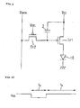
- FIG. 13 shows another driving circuit of an organic electroluminescent element.
- the driving circuit shown here is disclosed in Japanese Unexamined Patent Application Publication No. 11-272233.
- the driving circuit includes a driving transistor Tr 1 which supplies an electroluminescent element 10 with a current from a power source during the on state thereof, a capacitive element 2 which stores a charge for controlling the conduction state of the transistor Tr 1, and a charge control transistor Tr 5 which controls the charging of the capacitive element 2 in response to an external signal.
- a voltage V rscan is driven low to turn off a charge control transistor Tr 7 to cause the electroluminescent element 10 to emit light, and then, a reset signal V rsig is not output.
- a transistor Tr 6 is included for adjustment purposes.
- the transistor Tr 5 When the electroluminescent element 10 emits light in the driving circuit, the transistor Tr 5 is turned on, and the capacitive element 2 is charged by a transistor Tr 6 through a data line V DATA . Conductance between the source and drain of the transistor Tr 1 is controlled in response to a charge level of the capacitive element 2 to allow a current to flow through the electroluminescent element 10. Referring to FIG. 14, when the voltage V SCAN is driven high to turn on the transistor Tr 5, the capacitive element 2 is charged through the transistor Tr 6. Conductance between the source and drain of the transistor Tr 1 is controlled in response to a charge level of the capacitive element 2 to allow a current to flow through the electroluminescent element 10.
- Reverse-biasing the organic electroluminescent element is known as an effective means to prolong the service life of the organic electroluminescent element.
- Japanese Unexamined Patent Application Publication No. 11-8064 discloses a technique for prolonging the service life of the organic electroluminescent element.
- an additional power source for a negative voltage needs to be prepared and controlled to reverse-bias the organic electroluminescent element.
- a first driving circuit of the present invention drives an organic electroluminescent display device in which a plurality of pixels, each containing an organic electroluminescent element, is arranged in a matrix, and the first driving circuit includes a reverse-bias setting circuit which sets the organic electroluminescent elements in a reverse-bias state on an area-by-area basis.
- a second driving circuit of the present invention drives an organic electroluminescent display device in which a plurality of pixels, each containing an organic electroluminescent element, is arranged in a matrix, and the second driving circuit includes a reverse-bias setting circuit which sets organic electroluminescent elements contained in a predetermined area, from among the organic electroluminescent elements, in a reverse-bias state.
- the reverse-bias setting circuit includes a switch which switches an electrical connection state of at least one of electrodes of each of the organic electroluminescent elements between being connected to a first power source line for supplying a first voltage and being connected to a second power source line for supplying a second voltage that is lower in level than the first voltage.
- the switch Since the switch is used to switch the connection state of the driving circuit between being connected to a first power source and a second power source, no additional power is required. Without involving an increase in power consumption and a cost increase, a reverse-bias is supplied to the organic electroluminescent element.
- the first power source is Vcc
- the second power source is ground (GND).
- the reverse-bias setting circuit includes a switch which switches an electrical connection state of a cathode of each of the organic electroluminescent elements between being connected to a first power source line for supplying a first voltage and being connected to a second power source line for supplying a second voltage that is lower in level than the first voltage.
- the switches are arranged with one switch for each pixel, and the organic electroluminescent elements are set to be in a reverse-bias state on a pixel-by-pixel basis by controlling the switches.
- the switches are arranged with one switch for each line of pixels, and the organic electroluminescent elements are set to be in a reverse-bias state on a line-by-line basis by controlling the switches.
- the switch is arranged with the single switch for all pixels, and the organic electroluminescent elements of all pixels are set to be in a reverse-bias state by controlling the switch.
- the switches are arranged with one switch for each of particular pixels, and the organic electroluminescent elements of the particular pixels are set to be in a reverse-bias state by controlling the switches.
- a ninth driving circuit of the present invention drives an electro-optical device in which a plurality of electro-optical elements is arranged in a matrix, and includes a reverse-bias setting circuit which sets at least one of the electro-optical elements in a reverse-bias state.
- First electronic equipment of the present invention includes an active-matrix display device including the driving circuit.
- a first electro-optical device of the present invention includes a driving circuit for actively driving a display device in which a plurality of pixels, each including an electro-optical element, is arranged in a matrix, and the driving circuit includes a reverse-bias setting circuit which sets the electro-optical elements in a reverse-bias state on an area-by-area basis.
- a second electro-optical device of the present invention includes a driving circuit for driving a display device in which a plurality of pixels, each including an electro-optical element, is arranged in a matrix, and the driving circuit includes a reverse-bias setting circuit which sets electro-optical elements contained in a predetermined area, from among the electro-optical elements, in a reverse-bias state.
- the reverse-bias setting circuit includes a switch which switches an electrical connection state of at least one of electrodes of each of the electro-optical elements between being connected to a first power source line for supplying a first voltage and being connected to a second power source line for supplying a second voltage that is lower in level than the first voltage.
- the reverse-bias setting circuit includes a switch which switches an electrical connection state of a cathode of each of the electro-optical elements between being connected to a first power source line for supplying a first voltage and being connected to a second power source line for supplying a second voltage that is lower in level than the first voltage.
- the switches are arranged with one switch for each pixel, and the electro-optical elements are set to be in a reverse-bias state on a pixel-by-pixel basis by controlling the switches.
- the switches are arranged with one switch for each line of pixels, and the electro-optical elements are set to be in a reverse-bias state on a line-by-line basis by controlling the switches.
- the switch is arranged with the single switch for all pixels, and the organic electroluminescent elements of all pixels are set to be in a reverse-bias state by controlling the switch.
- the switches are arranged with one switch for each of particular pixels, and the electro-optical elements of the particular pixels are set to be in a reverse-bias state by controlling the switches.
- a ninth electro-optical device of the present invention includes a driving circuit for driving a matrix of electro-optical elements, wherein the driving circuit includes a reverse-bias setting circuit which sets at least one of the plurality of electro-optical elements in a reverse-bias state on an area-by-area basis.
- the electro-optical element is an organic electroluminescent element.
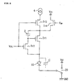
- FIG. 2 is a circuit diagram showing one embodiment of a driving circuit for an active-matrix display device that incorporates organic electroluminescent elements.
- the organic electroluminescent element driving circuit of this embodiment includes a switch 20 which switches the connection of the cathode of each organic electroluminescent element from a second potential (GND) to a first potential (Vcc). To cause the organic electroluminescent element 10 to emit light, the switch 20 is simply connected to the second potential (Vcc). This state is identical to the state shown in FIG. 9.
- the transistor Tr 1 is turned off and the switch 20 is set to connect the organic electroluminescent element 10 to the first potential (Vcc). Since the anode of the organic electroluminescent element 10 cannot be higher than the first potential (Vcc), the organic electroluminescent element 10 is reverse-biased.
- the anode of the organic electroluminescent element 10 rises in potential in response to a potential change in the cathode of the organic electroluminescent element 10, i.e., a potential rise from the second voltage (GND) to the first voltage (Vcc).
- the organic electroluminescent element 10 can not be applied with a sufficient reverse-bias voltage.
- a potential rise in the anode side must be restricted.
- Increasing a wiring parasitic capacitance C on the anode side is contemplated as a means to control the potential rise.
- a large reverse-bias voltage can be applied by increasing the parasitic capacitance C on the anode side, and degradation of the organic electroluminescent element 10 is thus effectively controlled.
- FIGS. 3(a)-3(b) A method of increasing the parasitic capacitance on the anode will now be discussed, referring to FIGS. 3(a)-3(b).
- FIGS. 3(a)-3(b) A typical cross-sectional construction of the organic electroluminescent element is first discussed, referring to FIG. 3(a).
- a semiconductor thin film is formed on a glass substrate 81.
- a source region 82 and a drain region 85 of a transistor are formed within the semiconductor thin film.
- a gate insulator layer 83 covers the source region 82 and the drain region 85 of the transistor.
- a gate electrode 84 is formed on the gate insulator layer 83.
- a first interlayer insulator 86 covers the gate electrode 84 and the gate insulator layer 83. Connection holes are drilled in the gate insulator layer 83 and the first interlayer insulator 86.
- the source region 82 and the drain region 85 are respectively connected to a source electrode 87 and a drain electrode 91 by filling the respective connection holes with an electrically conductive material.
- a second interlayer insulator 88 covers the source electrode 87, the drain electrode 91, and the first interlayer insulator 86.
- the drain electrode 91 is connected to an organic thin-film laminate, including an emission layer 95, through the anode 89 constructed of ITO.
- the organic thin-film laminate includes at least a hole injection layer 93 and the emission layer 95.
- a cathode 97 of the organic electroluminescent element is formed on the organic thin-film laminate.
- the switch 20 switches the potential of the cathode 97 from the second potential (GND) to the first potential (Vcc).
- a conductive member is arranged in the vicinity of wiring between the anode 89 of the organic electroluminescent element and the transistor to form a parasitic capacitance to the wiring.
- the parasitic capacitance C is increased by setting the separation between the source electrode 87 and the drain electrode 91 to be narrower than a typical distance, or by setting facing areas of these electrodes to be larger than the remaining areas. In other words, the parasitic capacitance C is set up between the source electrode and the drain electrode of the driving transistor.
- a metal layer 92 is arranged within the first interlayer insulator 86 to increase a parasitic capacitance between the metal layer 92 and the drain electrode 91.
- the parasitic capacitance C is set up between the metal layer 92 arranged within the first interlayer insulator 86 and the drain electrode 91.
- the organic electroluminescent element is put into an emission state or a reverse-bias state. No extra negative-voltage power source is required. This arrangement involves neither increase in power consumption nor additional space requirement.
- the switch 20 is easily constructed by combining a transistor.
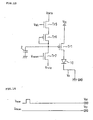
- the switch 20 is connected to the cathode of the organic electroluminescent element 10.
- the organic electroluminescent element 10 is set to be in the reverse-bias state using the parasitic capacitance in the same way as in the circuit shown in FIG. 2.
- the above-mentioned driving circuit shown in FIG. 13 may include the switch 20 to the cathode of the organic electroluminescent element 10 in the same way as in the circuit shown in FIG. 5.
- the switch 20 switches the cathode of the organic electroluminescent element from the first potential (Vcc) to the second potential (GND).
- Vcc first potential
- GND second potential
- the organic electroluminescent element 10 is easily put into the reverse-bias state.
- the organic electroluminescent element When a display device is constructed of the organic electroluminescent elements, the organic electroluminescent element corresponds to a single pixel. In the arrangements shown in FIG. 2 through FIG. 5, a switch is required for each organic electroluminescent element, i.e., for each pixel.
- FIG. 1 shows the connection of pixel circuits 1-1, 1-2, ..., each having the respective organic electroluminescent element, with the corresponding switches 20-1, 20-2, ....
- the pixel circuit 1-1 having the respective organic electroluminescent element is provided with the switch 20-1, and the pixel circuit 1-2 is provided with the switch 20-2.
- one pixel has its own switch having the above-referenced structure. These switches are respectively controlled by control signals S1 and S2.
- the control signals are input for a period of time except a duration of time during which the capacitor in each pixel circuit is charged and except a duration of time during which the organic electroluminescent element 10 emits light, thereby controlling the respective switches.
- a control signal S is easily generated referencing the selection voltage V SEL that determines the write period T W and the data hold control signal V gp that determines the display period T H .
- the time other than the write period T W determined by the selection voltage V SEL and the display period T H determined by the data hold control signal V gp becomes a reverse-bias period T B .
- the above-referenced switch may be arranged for each line of pixels forming a display screen.
- a switch 20-1 is arranged so that it is shared by pixel circuits 1-11, 1-12, ... and a switch 20-2 is arranged so that it is shared by pixel circuits 1-21, 1-22, ....
- the number of switches is smaller than in the circuit shown in FIG. 1. It is possible to reduce costs.
- the pixels are reverse-biased on a line-by-line basis as shown in FIG. 6(b), a given line of pixels is in the reverse-bias period T B , and the remaining lines of pixels are in either write period T W or the display period T H . Since a plurality of lines forming the display screen is provided with the respective switches, the pixels are periodically set to be in the reverse-bias state on a line-by-line basis. The service life of the organic electroluminescent element is thus prolonged.
- a given line may be in the reverse-bias period T W or the write period T W , and the remaining lines may be in the display period T H .
- a single switch is arranged for all pixels forming the display screen. By controlling the switch, the organic electroluminescent elements for all pixels forming the display screen are concurrently put into the reverse-bias state.
- a single switch 20 is shared by pixel circuits 1-11, 1-12, ..., and pixel circuits 1-21, 1-22, ..., and the switch 20 concurrently sets all pixels to be in the reverse-bias state.
- the single switch is shared by all pixels, the number of switches is minimized, which makes it possible to reduce costs.
- the time length of the reverse-bias period T B is set so that the write period T W and the display period T H equal each other in one frame period F.
- the reverse-bias period T B comes first at the beginning of the frame period, followed by the write period T W and the display period T H .
- the reverse-bias period T B may be at any position within the frame period F.
- a color display device employs the organic electroluminescent elements
- particular organic electroluminescent materials for emitting light of different colors such as red, green, and blue may be used.
- different organic electroluminescent materials there occurs a difference in service life therebetween.
- any organic electroluminescent material having the shortest service life determines the service life of the display device. Reverse-biasing the particular pixels only is thus contemplated. In this case, the following two methods are available. (i) Only organic electroluminescent elements for the pixels having shorter life are reverse-biased.
- the number of times a reverse bias is applied to the organic electroluminescent elements for the pixels having shorter life is set to be larger than the number of times the remaining organic electroluminescent elements will be reverse-biased. In this way, the service life of the entire display screen can be prolonged.
- Some organic electroluminescent display device produces an area display that is presented on a portion of the display screen in a particular color, such as orange, blue, green, etc.
- a display device only the organic electroluminescent elements having the shortest display life area may be reverse-biased. In this way, the service life of the display screen can be prolonged.
- the driving circuit for the active-matrix display device that uses the organic electroluminescent elements has been discussed.
- the present invention is not limited to this type of display device only.
- the present invention may be applied to an active-matrix display device employing an electro-optical element, other than the organic electroluminescent element, such as a TFT-LCD, an FED (Field Emission Display), an electrophoresis element, an electric field reversing element, a laser diode, or an LED.
- FIG. 15 shows a perspective view showing the construction of a mobile personal computer 1100 incorporating the active-matrix display device.
- the personal computer 1100 includes a main unit 1104 with a keyboard 1102, and a display unit 1106.
- the display unit 1106 includes the active-matrix display device 100
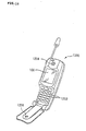
- FIG. 16 is a perspective view showing the construction of a mobile telephone 1200 which incorporates the active-matrix display device 100 including the above-referenced driving circuit.
- the mobile telephone 1200 includes a plurality of control buttons 1202, an ear piece 1204, a mouth piece 1206, and the active-matrix display device 100.
- FIG. 17 is a perspective view showing the construction of a digital still camera 1300 which incorporates the active-matrix display device 100, including the above-reference driving circuit, as a viewfinder.
- the digital still camera 1300 In contrast with a silver-film camera that exposes a film to an optical image of an object, the digital still camera 1300 generates a video signal by photoelectrically converting an optical image of an object through an image pickup device such as a CCD (Charge-Coupled Device).
- the above-referenced active-matrix display device 100 is mounted on the back of a case 1302 of the digital still camera 1300.
- the active-matrix display device 100 functions as a view finder to display the image of the object.
- a photodetector unit 1304 Arranged on the front of the case 1302 (the far side of the case 1302 in FIG. 17) is a photodetector unit 1304 including an optical lens and the CCD.
- the digital still camera 1300 is provided on the side of the case 1302 with a video signal output terminal 1312 and an input/output terminal 1314 for data exchange.
- a television monitor 1430 is connected to the video signal output terminal 1312
- a personal computer 1440 is connected to the input/output terminal 1314 for data exchange.
- the video signal stored in the memory of the circuit board 1308 is output to the television monitor 1430 and the personal computer 1430.
- the electronic equipment to which the active-matrix display device 100 of the present invention is applied may be any of a diversity of electronic equipment including a liquid-crystal display television, a viewfinder type or direct monitoring type video cassette recorder, a car navigation system, a pager, an electronic pocketbook, an electronic tabletop calculator, a word processor, a workstation, a video phone, a POS terminal, and an apparatus having a touch panel.
- the above-referenced active-matrix display device 100 is used as a display unit in each of the above electronic equipment.
- the organic electroluminescent elements are set to be in the reverse-bias state on the basis of a group of predetermined pixels at a time, and the reverse-bias voltage can be applied without involving an increase in power consumption and an increase in layout space requirement.
- the service life of the organic electroluminescent element can be thus prolonged.
- the reverse-bias voltage can be applied without the need for an additional power source.
- the service life of the organic electroluminescent element can be further prolonged.
Abstract
Description
- The present invention relates to a driving circuit for driving an active-matrix display device employing organic electroluminescent elements, and electronic equipment and an electro-optical device, incorporating the driving circuit, and, more particularly, to a driving circuit having the function of applying a reverse-bias voltage to an organic electroluminescent element for controlling degradation of the organic electroluminescent element, and electronic equipment and an electro-optical device, incorporating the driving circuit.
- It is known that an organic EL display device is produced by arranging a plurality of pixels of organic electroluminescent elements, i.e., one of electro-optical elements, in a matrix. The organic electroluminescent element includes a metal electrode of Mg:Ag or A1:Li, etc., as a cathode, a transparent electrode such as an ITO (Indium Tin Oxide) as an anode, and an organic thin-film laminate, including an emission layer, interposed between the cathode and the anode.
- FIG. 9 shows a typical construction of a driving circuit for an active matrix display device employing an organic electroluminescent element. Referring to FIG. 9, the organic electroluminescent element is shown as a
diode 10. The driving circuit is composed of transistors Tr 1 andTr 2, each constructed of a thin-film transistor (TFT), and acapacitive element 2 storing charge. - Both the transistor Tr 1 and the
transistor Tr 2 are of a p-channel TFT. The conduction state of the transistor Tr 1 is controlled in response to a charge stored in thecapacitive element 2 as shown. Thecapacitive element 2 is charged through a data line VDATA by thetransistor Tr 2, which is turned on with a selection voltage VSEL driven low. When the transistor Tr 1 is turned on, a current flows through theelectroluminescent element 10 from the transistor Tr 1. With the current flowing therethrough, theelectroluminescent element 10 continuously emits light. - FIG. 10 shows a simple timing diagram for the circuit shown in FIG. 9. When data is written, the selection voltage VSEL is driven low as shown FIG. 10. The
transistor Tr 2 is turned on, thus charging thecapacitive element 2. The charge duration is a write period TW. An actual presentation period follows the write period TW. During the presentation period, charge stored in thecapacitive element 2 controls the conduction state of the transistor Tr 1. The presentation period is represented by TH as shown. - FIG. 11 shows another arrangement of the organic electroluminescent element driving circuit. The driving circuit shown is described in a paper entitled "The Impact of Transient Response of Organic Light Emitting Diodes on the Design of Active Matrix OLED Displays" (1998 IEEE IEDM98-875). Referring to FIG. 11, there are shown a driving transistor Tr 1, a charge
control transistor Tr 2, a first selection transistor Tr 3, and a second selection transistor Tr 4 which is turned off during a charging period of thecapacitive element 2. - As is well known, transistors, even complying with the same specifications, suffer variations in performance. Even when the same voltage is applied to the gates of transistors, these transistor do not necessarily permit current of equal values to flow therethrough. Such variations cause nonuniformity in brightness. In the driving circuit, a current source 4 feeds a write current corresponding to a data signal, and the data signal thus controls the gate voltage of the transistor. In this way, the emission state of the organic electroluminescent element is controlled.
- Transistors Tr 1 through Tr 4 are all of a p-type channel transistor. When the selection voltage VSEL is driven low, the
transistors Tr 2 and Tr 3 are turned on, thereby storing in the capacitive element 2 a charge corresponding to the value of the output of the current source 4. When the selection voltage VSEL is driven high, thetransistors Tr 2 and Tr 3 are turned off. The conduction state of the transistor Tr 1 is thus controlled by the charge stored in thecapacitive element 2. With a data hold control signal Vgp turning on the transistor Tr 4, anelectroluminescent element 10 is supplied with a current corresponding to the charge stored in thecapacitive element 2. This duration of time is a presentation period TH. - FIG. 12 shows a simple timing diagram of the circuit shown in FIG. 11. When data writing is performed by the current source 4 as shown in FIG. 12, the selection voltage VSEL is driven low, thereby turning on the
transistors Tr 2 and Tr 3. Thecapacitive element 2 is thus charged. The charge period equals a write period TW. With the selection voltage VSEL driven high, thetransistors Tr 2 and Tr 3 are turned off. With the data hold control signal Vgp driven low, the conduction state of the transistor Tr 1 is determined based on the charge stored in thecapacitive element 2. Theelectroluminescent element 10 is supplied with a current corresponding to the charge stored in thecapacitive element 2. This duration of time is a presentation period TH. - FIG. 13 shows another driving circuit of an organic electroluminescent element. The driving circuit shown here is disclosed in Japanese Unexamined Patent Application Publication No. 11-272233. As shown, the driving circuit includes a driving transistor Tr 1 which supplies an
electroluminescent element 10 with a current from a power source during the on state thereof, acapacitive element 2 which stores a charge for controlling the conduction state of the transistor Tr 1, and a charge control transistor Tr 5 which controls the charging of thecapacitive element 2 in response to an external signal. A voltage Vrscan is driven low to turn off a charge control transistor Tr 7 to cause theelectroluminescent element 10 to emit light, and then, a reset signal Vrsig is not output. A transistor Tr 6 is included for adjustment purposes. - When the
electroluminescent element 10 emits light in the driving circuit, the transistor Tr 5 is turned on, and thecapacitive element 2 is charged by a transistor Tr 6 through a data line VDATA. Conductance between the source and drain of the transistor Tr 1 is controlled in response to a charge level of thecapacitive element 2 to allow a current to flow through theelectroluminescent element 10. Referring to FIG. 14, when the voltage VSCAN is driven high to turn on the transistor Tr 5, thecapacitive element 2 is charged through the transistor Tr 6. Conductance between the source and drain of the transistor Tr 1 is controlled in response to a charge level of thecapacitive element 2 to allow a current to flow through theelectroluminescent element 10. - Reverse-biasing the organic electroluminescent element is known as an effective means to prolong the service life of the organic electroluminescent element. For example, Japanese Unexamined Patent Application Publication No. 11-8064 discloses a technique for prolonging the service life of the organic electroluminescent element.
- To reverse-bias the organic electroluminescent element using the disclosed technique, an additional power source for a negative voltage needs to be prepared and controlled to reverse-bias the organic electroluminescent element.
- It is an object of the present invention to provide a driving circuit, for driving an organic electroluminescent element, which supplies the organic electroluminescent element with a reverse bias without involving an increase in power consumption and a cost increase, and to provide electronic equipment, and an electro-optical device.
- A first driving circuit of the present invention drives an organic electroluminescent display device in which a plurality of pixels, each containing an organic electroluminescent element, is arranged in a matrix, and the first driving circuit includes a reverse-bias setting circuit which sets the organic electroluminescent elements in a reverse-bias state on an area-by-area basis.
- A second driving circuit of the present invention drives an organic electroluminescent display device in which a plurality of pixels, each containing an organic electroluminescent element, is arranged in a matrix, and the second driving circuit includes a reverse-bias setting circuit which sets organic electroluminescent elements contained in a predetermined area, from among the organic electroluminescent elements, in a reverse-bias state.
- In a third driving circuit of the present invention, the reverse-bias setting circuit includes a switch which switches an electrical connection state of at least one of electrodes of each of the organic electroluminescent elements between being connected to a first power source line for supplying a first voltage and being connected to a second power source line for supplying a second voltage that is lower in level than the first voltage.
- Since the switch is used to switch the connection state of the driving circuit between being connected to a first power source and a second power source, no additional power is required. Without involving an increase in power consumption and a cost increase, a reverse-bias is supplied to the organic electroluminescent element. In this case, typically, the first power source is Vcc, and the second power source is ground (GND). These are existing power sources. The present invention is not limited to this arrangement, as long as a voltage difference large enough to cause the organic electroluminescent element to emit light is used.
- In a fourth driving circuit of the present invention, the reverse-bias setting circuit includes a switch which switches an electrical connection state of a cathode of each of the organic electroluminescent elements between being connected to a first power source line for supplying a first voltage and being connected to a second power source line for supplying a second voltage that is lower in level than the first voltage.
- In a fifth driving circuit of the present invention, the switches are arranged with one switch for each pixel, and the organic electroluminescent elements are set to be in a reverse-bias state on a pixel-by-pixel basis by controlling the switches.
- In a sixth driving circuit of the present invention, the switches are arranged with one switch for each line of pixels, and the organic electroluminescent elements are set to be in a reverse-bias state on a line-by-line basis by controlling the switches.
- In a seventh driving circuit of the present invention, the switch is arranged with the single switch for all pixels, and the organic electroluminescent elements of all pixels are set to be in a reverse-bias state by controlling the switch.
- In an eighth driving circuit of the present invention, the switches are arranged with one switch for each of particular pixels, and the organic electroluminescent elements of the particular pixels are set to be in a reverse-bias state by controlling the switches.
- A ninth driving circuit of the present invention drives an electro-optical device in which a plurality of electro-optical elements is arranged in a matrix, and includes a reverse-bias setting circuit which sets at least one of the electro-optical elements in a reverse-bias state.
- First electronic equipment of the present invention includes an active-matrix display device including the driving circuit.
- A first electro-optical device of the present invention includes a driving circuit for actively driving a display device in which a plurality of pixels, each including an electro-optical element, is arranged in a matrix, and the driving circuit includes a reverse-bias setting circuit which sets the electro-optical elements in a reverse-bias state on an area-by-area basis.
- A second electro-optical device of the present invention includes a driving circuit for driving a display device in which a plurality of pixels, each including an electro-optical element, is arranged in a matrix, and the driving circuit includes a reverse-bias setting circuit which sets electro-optical elements contained in a predetermined area, from among the electro-optical elements, in a reverse-bias state.
- In a third electro-optical device of the present invention, the reverse-bias setting circuit includes a switch which switches an electrical connection state of at least one of electrodes of each of the electro-optical elements between being connected to a first power source line for supplying a first voltage and being connected to a second power source line for supplying a second voltage that is lower in level than the first voltage.
- In a fourth electro-optical device of the present invention, the reverse-bias setting circuit includes a switch which switches an electrical connection state of a cathode of each of the electro-optical elements between being connected to a first power source line for supplying a first voltage and being connected to a second power source line for supplying a second voltage that is lower in level than the first voltage.
- In a fifth electro-optical device of the present invention, the switches are arranged with one switch for each pixel, and the electro-optical elements are set to be in a reverse-bias state on a pixel-by-pixel basis by controlling the switches.
- In a sixth electro-optical device of the present invention, the switches are arranged with one switch for each line of pixels, and the electro-optical elements are set to be in a reverse-bias state on a line-by-line basis by controlling the switches.
- In a seventh electro-optical device of the present invention, the switch is arranged with the single switch for all pixels, and the organic electroluminescent elements of all pixels are set to be in a reverse-bias state by controlling the switch.
- In an eighth electro-optical device of the present invention, the switches are arranged with one switch for each of particular pixels, and the electro-optical elements of the particular pixels are set to be in a reverse-bias state by controlling the switches.
- A ninth electro-optical device of the present invention includes a driving circuit for driving a matrix of electro-optical elements, wherein the driving circuit includes a reverse-bias setting circuit which sets at least one of the plurality of electro-optical elements in a reverse-bias state on an area-by-area basis.
- In a tenth electro-optical device of the present invention, the electro-optical element is an organic electroluminescent element.
- Embodiments of the present invention will now be described by way of further example only and with reference to the accompanying drawings, in which:-
- FIG. 1 is a circuit diagram showing a driving circuit for driving organic electroluminescent elements in accordance with one embodiment of the present invention.
- FIG. 2 is a circuit diagram showing the construction of the organic electroluminescent element driving circuit of the present invention.
- FIG. 3 is a cross-sectional view of a pixel circuit in the organic electroluminescent element driving circuit of the present invention.
- FIG. 4 is a circuit diagram showing another arrangement of the organic electroluminescent element driving circuit of the present invention.
- FIG. 5 is a circuit diagram showing still another arrangement of the organic electroluminescent element driving circuit of the present invention.
- FIG. 6 is a waveform diagram showing the operation of the organic electroluminescent element driving circuit of the present invention.
- FIG. 7 is a circuit diagram showing another embodiment of the organic electroluminescent element driving circuit of the present invention.
- FIG. 8 is a circuit diagram showing still another embodiment of the organic electroluminescent element driving circuit of the present invention.
- FIG. 9 is a circuit diagram showing the construction of a conventional organic electroluminescent element driving circuit.
- FIG. 10 is a waveform diagram showing the operation of the organic electroluminescent element driving circuit shown in FIG. 9.
- FIG. 11 is a circuit diagram showing the construction of another conventional organic electroluminescent element driving circuit.
- FIG. 12 is a waveform diagram showing the operation of the organic electroluminescent element driving circuit shown in FIG. 11.
- FIG. 13 is a circuit diagram showing the construction of yet another conventional organic electroluminescent element driving circuit.
- FIG. 14 is a waveform diagram showing the operation of the organic electroluminescent element driving circuit shown in FIG. 13.
- FIG. 15 is a perspective view showing the construction of a mobile personal computer as one example of electronic equipment that incorporates an active-matrix display device including a driving circuit of one embodiment of the present invention.
- FIG. 16 is a perspective view showing the construction of a mobile telephone as one example of the electronic equipment that incorporates an active-matrix display device including a driving circuit of one embodiment of the present invention.
- FIG. 17 is a perspective view showing the construction of a digital still camera as one example of the electronic equipment that incorporates an active-matrix display device including a driving circuit of one embodiment of the present invention.
-
- The embodiments of the present invention will now be discussed, referring to the accompanying drawings. Like components are identified with like reference numerals throughout the drawings.
- FIG. 2 is a circuit diagram showing one embodiment of a driving circuit for an active-matrix display device that incorporates organic electroluminescent elements. Referring to FIG. 2, the organic electroluminescent element driving circuit of this embodiment includes a
switch 20 which switches the connection of the cathode of each organic electroluminescent element from a second potential (GND) to a first potential (Vcc). To cause theorganic electroluminescent element 10 to emit light, theswitch 20 is simply connected to the second potential (Vcc). This state is identical to the state shown in FIG. 9. - To apply a reverse bias to the
organic electroluminescent element 10, the transistor Tr 1 is turned off and theswitch 20 is set to connect theorganic electroluminescent element 10 to the first potential (Vcc). Since the anode of theorganic electroluminescent element 10 cannot be higher than the first potential (Vcc), theorganic electroluminescent element 10 is reverse-biased. - When the parasitic capacitance C of the anode of the
organic electroluminescent element 10 is small, the anode of theorganic electroluminescent element 10 rises in potential in response to a potential change in the cathode of theorganic electroluminescent element 10, i.e., a potential rise from the second voltage (GND) to the first voltage (Vcc). As a result, theorganic electroluminescent element 10 can not be applied with a sufficient reverse-bias voltage. To apply a sufficient reverse-bias voltage, a potential rise in the anode side must be restricted. Increasing a wiring parasitic capacitance C on the anode side is contemplated as a means to control the potential rise. A large reverse-bias voltage can be applied by increasing the parasitic capacitance C on the anode side, and degradation of theorganic electroluminescent element 10 is thus effectively controlled. - A method of increasing the parasitic capacitance on the anode will now be discussed, referring to FIGS. 3(a)-3(b). A typical cross-sectional construction of the organic electroluminescent element is first discussed, referring to FIG. 3(a).
- A semiconductor thin film is formed on a
glass substrate 81. Asource region 82 and adrain region 85 of a transistor are formed within the semiconductor thin film. Agate insulator layer 83 covers thesource region 82 and thedrain region 85 of the transistor. Agate electrode 84 is formed on thegate insulator layer 83. Afirst interlayer insulator 86 covers thegate electrode 84 and thegate insulator layer 83. Connection holes are drilled in thegate insulator layer 83 and thefirst interlayer insulator 86. Thesource region 82 and thedrain region 85 are respectively connected to asource electrode 87 and adrain electrode 91 by filling the respective connection holes with an electrically conductive material. Asecond interlayer insulator 88 covers thesource electrode 87, thedrain electrode 91, and thefirst interlayer insulator 86. Thedrain electrode 91 is connected to an organic thin-film laminate, including anemission layer 95, through theanode 89 constructed of ITO. The organic thin-film laminate includes at least ahole injection layer 93 and theemission layer 95. Acathode 97 of the organic electroluminescent element is formed on the organic thin-film laminate. Theswitch 20 switches the potential of thecathode 97 from the second potential (GND) to the first potential (Vcc). - The method of increasing the parasitic capacitance on the anode will now be detailed.
- A conductive member is arranged in the vicinity of wiring between the
anode 89 of the organic electroluminescent element and the transistor to form a parasitic capacitance to the wiring. Specifically, referring to FIG. 3(b), the parasitic capacitance C is increased by setting the separation between thesource electrode 87 and thedrain electrode 91 to be narrower than a typical distance, or by setting facing areas of these electrodes to be larger than the remaining areas. In other words, the parasitic capacitance C is set up between the source electrode and the drain electrode of the driving transistor. - Referring to FIG. 3(c), a
metal layer 92 is arranged within thefirst interlayer insulator 86 to increase a parasitic capacitance between themetal layer 92 and thedrain electrode 91. Specifically, the parasitic capacitance C is set up between themetal layer 92 arranged within thefirst interlayer insulator 86 and thedrain electrode 91. - By simply resetting the
switch 20, the organic electroluminescent element is put into an emission state or a reverse-bias state. No extra negative-voltage power source is required. This arrangement involves neither increase in power consumption nor additional space requirement. Theswitch 20 is easily constructed by combining a transistor. - Referring to FIG. 4, the
switch 20 is connected to the cathode of theorganic electroluminescent element 10. When theswitch 20 is turned to the first potential (Vcc) from the second potential (GND), theorganic electroluminescent element 10 is set to be in the reverse-bias state using the parasitic capacitance in the same way as in the circuit shown in FIG. 2. - The above-mentioned driving circuit shown in FIG. 13 may include the
switch 20 to the cathode of theorganic electroluminescent element 10 in the same way as in the circuit shown in FIG. 5. Theswitch 20 switches the cathode of the organic electroluminescent element from the first potential (Vcc) to the second potential (GND). Using the parasitic capacitance C, theorganic electroluminescent element 10 is easily put into the reverse-bias state. - When a display device is constructed of the organic electroluminescent elements, the organic electroluminescent element corresponds to a single pixel. In the arrangements shown in FIG. 2 through FIG. 5, a switch is required for each organic electroluminescent element, i.e., for each pixel.
- FIG. 1 shows the connection of pixel circuits 1-1, 1-2, ..., each having the respective organic electroluminescent element, with the corresponding switches 20-1, 20-2, ....
- As shown, the pixel circuit 1-1 having the respective organic electroluminescent element is provided with the switch 20-1, and the pixel circuit 1-2 is provided with the switch 20-2. Specifically, one pixel has its own switch having the above-referenced structure. These switches are respectively controlled by control signals S1 and S2. The control signals are input for a period of time except a duration of time during which the capacitor in each pixel circuit is charged and except a duration of time during which the
organic electroluminescent element 10 emits light, thereby controlling the respective switches. In the embodiment shown in FIG. 4, a control signal S is easily generated referencing the selection voltage VSEL that determines the write period TW and the data hold control signal Vgp that determines the display period TH. Specifically, as shown in FIG. 6(a), the time other than the write period TW determined by the selection voltage VSEL and the display period TH determined by the data hold control signal Vgp becomes a reverse-bias period TB. - The above-referenced switch may be arranged for each line of pixels forming a display screen. Referring to FIG. 7, a switch 20-1 is arranged so that it is shared by pixel circuits 1-11, 1-12, ... and a switch 20-2 is arranged so that it is shared by pixel circuits 1-21, 1-22, .... When one switch is arranged for each line, the number of switches is smaller than in the circuit shown in FIG. 1. It is possible to reduce costs.
- If the pixels are reverse-biased on a line-by-line basis as shown in FIG. 6(b), a given line of pixels is in the reverse-bias period TB, and the remaining lines of pixels are in either write period TW or the display period TH. Since a plurality of lines forming the display screen is provided with the respective switches, the pixels are periodically set to be in the reverse-bias state on a line-by-line basis. The service life of the organic electroluminescent element is thus prolonged.
- In the pixel circuit that permits the reverse-bias period TB and the write period TW to concurrently take place as shown in FIG. 6(c), a given line may be in the reverse-bias period TW or the write period TW, and the remaining lines may be in the display period TH.
- A single switch is arranged for all pixels forming the display screen. By controlling the switch, the organic electroluminescent elements for all pixels forming the display screen are concurrently put into the reverse-bias state. Referring to FIG. 8, a
single switch 20 is shared by pixel circuits 1-11, 1-12, ..., and pixel circuits 1-21, 1-22, ..., and theswitch 20 concurrently sets all pixels to be in the reverse-bias state. When the single switch is shared by all pixels, the number of switches is minimized, which makes it possible to reduce costs. - When all pixels are concurrently set to be in the reverse-bias state as shown in FIG. 6(d), the time length of the reverse-bias period TB is set so that the write period TW and the display period TH equal each other in one frame period F. Referring to FIG. 6(d), the reverse-bias period TB comes first at the beginning of the frame period, followed by the write period TW and the display period TH. Alternatively, the reverse-bias period TB may be at any position within the frame period F.
- If a color display device employs the organic electroluminescent elements, particular organic electroluminescent materials for emitting light of different colors such as red, green, and blue may be used. When different organic electroluminescent materials are employed, there occurs a difference in service life therebetween. When the display device is constructed of a plurality of organic electroluminescent materials, any organic electroluminescent material having the shortest service life determines the service life of the display device. Reverse-biasing the particular pixels only is thus contemplated. In this case, the following two methods are available. (i) Only organic electroluminescent elements for the pixels having shorter life are reverse-biased. (ii) The number of times a reverse bias is applied to the organic electroluminescent elements for the pixels having shorter life is set to be larger than the number of times the remaining organic electroluminescent elements will be reverse-biased. In this way, the service life of the entire display screen can be prolonged.
- Some organic electroluminescent display device produces an area display that is presented on a portion of the display screen in a particular color, such as orange, blue, green, etc. In such a display device, only the organic electroluminescent elements having the shortest display life area may be reverse-biased. In this way, the service life of the display screen can be prolonged.
- The driving circuit for the active-matrix display device that uses the organic electroluminescent elements has been discussed. The present invention is not limited to this type of display device only. For example, the present invention may be applied to an active-matrix display device employing an electro-optical element, other than the organic electroluminescent element, such as a TFT-LCD, an FED (Field Emission Display), an electrophoresis element, an electric field reversing element, a laser diode, or an LED.
- Several pieces of electronic equipment incorporating the active-matrix display device including the above-referenced driving circuit 1 will now be discussed. FIG. 15 shows a perspective view showing the construction of a mobile
personal computer 1100 incorporating the active-matrix display device. As shown, thepersonal computer 1100 includes amain unit 1104 with a keyboard 1102, and adisplay unit 1106. Thedisplay unit 1106 includes the active-matrix display device 100 - FIG. 16 is a perspective view showing the construction of a
mobile telephone 1200 which incorporates the active-matrix display device 100 including the above-referenced driving circuit. As shown, themobile telephone 1200 includes a plurality ofcontrol buttons 1202, anear piece 1204, amouth piece 1206, and the active-matrix display device 100. - FIG. 17 is a perspective view showing the construction of a
digital still camera 1300 which incorporates the active-matrix display device 100, including the above-reference driving circuit, as a viewfinder. A simplified diagram of connections with external devices is also shown here. In contrast with a silver-film camera that exposes a film to an optical image of an object, thedigital still camera 1300 generates a video signal by photoelectrically converting an optical image of an object through an image pickup device such as a CCD (Charge-Coupled Device). The above-referenced active-matrix display device 100 is mounted on the back of acase 1302 of thedigital still camera 1300. The active-matrix display device 100 functions as a view finder to display the image of the object. Arranged on the front of the case 1302 (the far side of thecase 1302 in FIG. 17) is aphotodetector unit 1304 including an optical lens and the CCD. - When a photographer presses a
shutter button 1306 after recognizing the image of an object displayed on the active-matrix display device 100, the image taken by the CCD at the moment is transferred to and stored in a memory on acircuit board 1308. Thedigital still camera 1300 is provided on the side of thecase 1302 with a videosignal output terminal 1312 and an input/output terminal 1314 for data exchange. As shown, as required, atelevision monitor 1430 is connected to the videosignal output terminal 1312, and apersonal computer 1440 is connected to the input/output terminal 1314 for data exchange. In response to predetermined operational steps, the video signal stored in the memory of thecircuit board 1308 is output to thetelevision monitor 1430 and thepersonal computer 1430. - Besides the personal computer shown in FIG. 15, the mobile telephone shown in FIG. 16, and the digital still camera shown in FIG. 17, the electronic equipment to which the active-
matrix display device 100 of the present invention is applied may be any of a diversity of electronic equipment including a liquid-crystal display television, a viewfinder type or direct monitoring type video cassette recorder, a car navigation system, a pager, an electronic pocketbook, an electronic tabletop calculator, a word processor, a workstation, a video phone, a POS terminal, and an apparatus having a touch panel. The above-referenced active-matrix display device 100 is used as a display unit in each of the above electronic equipment. - In accordance with the present invention, the organic electroluminescent elements are set to be in the reverse-bias state on the basis of a group of predetermined pixels at a time, and the reverse-bias voltage can be applied without involving an increase in power consumption and an increase in layout space requirement. The service life of the organic electroluminescent element can be thus prolonged. Using the parasitic capacitance, the reverse-bias voltage can be applied without the need for an additional power source. The service life of the organic electroluminescent element can be further prolonged.
Claims (20)
- A driving circuit for actively driving an organic electroluminescent display device in which a plurality of pixels, each containing an organic electroluminescent element, are arranged in a matrix, the driving circuit comprising a reverse-bias setting circuit which sets the organic electroluminescent elements to a reverse-bias state on an area-by-area basis.
- A driving circuit for actively driving an organic electroluminescent display device in which a plurality of pixels, each containing an organic electroluminescent element, are arranged in a matrix, the driving circuit comprising a reverse-bias setting circuit which sets organic electroluminescent elements contained in a predetermined area, from among the organic electroluminescent elements, to a reverse-bias state.
- A driving circuit according to one of claims 1 and 2, wherein the reverse-bias setting circuit comprises a switch which switches an electrical connection state of at least one of electrodes of each of the organic electroluminescent elements between being connected to a first power source line for supplying a first potential and being connected to a second power source line for supplying a second potential that is lower in level than the first potential.
- A driving circuit according to one of claims 1 and 2, wherein the reverse-bias setting circuit comprises a switch which switches an electrical connection state of a cathode of each of the organic electroluminescent elements between being connected to a first power source line for supplying a first potential and being connected to a second power source line for supplying a second potential that is lower in level than the first potential.
- A driving circuit according to one of claims 3 and 4, wherein the switches are arranged with one switch for each pixel, so that the organic electroluminescent elements are set to be in a reverse-bias state on a pixel-by-pixel basis by controlling the switches.
- A driving circuit according to one of claims 3 through 5, wherein the switches are arranged with one switch for each line of pixels, so that the organic electroluminescent elements are set to be in a reverse-bias state on a line-by-line basis by controlling the switches.
- A driving circuit according to one of claims 3 and 4, wherein the switch is arranged with a single switch for all pixels, so that the organic electroluminescent elements for all pixels are set to be in a reverse-bias state by controlling the switch.
- A driving circuit according to one of claims 3 and 4, wherein the switches are arranged with one switch for each of particular pixels, so that only the organic electroluminescent elements for the particular pixels are set to be in a reverse-bias state by controlling the switches.
- A driving circuit for driving an electro-optical device in which a plurality of electro-optical elements are arranged in a matrix, the driving circuit comprising a reverse-bias setting circuit which sets at least one of the electro-optical elements to a reverse-bias state.
- Electronic equipment comprising an active-matrix display device mounted therein that includes the driving circuit according to one of claims 1 through 6.
- An electro-optical device comprising a driving circuit for actively driving a display device in which a plurality of pixels, each including an electro-optical element, are arranged in a matrix, the driving circuit comprising a reverse-bias setting circuit which sets the electro-optical elements to a reverse-bias state on a predetermined area-by-area basis.
- An electro-optical device comprising a driving circuit for actively driving a display device in which a plurality of pixels, each including an electro-optical element, are arranged in a matrix, the driving circuit comprising a reverse-bias setting circuit which sets electro-optical elements contained in a predetermined area, from among the electro-optical elements, to a reverse-bias state.
- An electro-optical device according to one of claims 11 and 12, wherein the reverse-bias setting circuit comprises a switch which switches an electrical connection state of at least one of electrodes of each of the electro-optical elements between being connected to a first power source line for supplying a first potential and being connected to a second power source line for supplying a second potential that is lower in level than the first potential.
- An electro-optical device according to one of claims 11 and 12, wherein the reverse-bias setting circuit comprises a switch which switches an electrical connection state of a cathode of each of the electro-optical elements between being connected to a first power source line for supplying a first potential and being connected to a second power source line for supplying a second potential that is lower in level than the first potential.
- An electro-optical device according to one of claims 13 and 14, wherein the switches are arranged with one switch for each pixel, so that the electro-optical elements are set to be in a reverse-bias state on a pixel-by-pixel basis by controlling the switches.
- An electro-optical device according to one of claims 13 through 15, wherein the switches are arranged with one switch for each line of pixels, so that the electro-optical elements are set to be in a reverse-bias state on a line-by-line basis by controlling the switches.
- An electro-optical device according to one of claims 13 and 14, wherein the switch is arranged with a single switch for all pixels, so that the organic electroluminescent elements for all pixels are set to be in a reverse-bias state by controlling the switch.
- An electro-optical device according to one of claims 13 and 14, wherein the switches are arranged with one switch for each of particular pixels, so that only the electro-optical elements for the particular pixels are set to be in a reverse-bias state by controlling the switches.
- An electro-optical device comprising a driving circuit for driving a plurality of electro-optical elements arranged in a matrix, wherein the driving circuit comprises a reverse-bias setting circuit which sets at least one of the plurality of electro-optical elements to a reverse-bias state on an area-by-area basis.
- An electro-optical device according to one of claims 11 through 19, wherein the electro-optical element is an organic electroluminescent element.
Applications Claiming Priority (4)
| Application Number | Priority Date | Filing Date | Title |
|---|---|---|---|
| JP2000312391 | 2000-10-12 | ||
| JP2000312391 | 2000-10-12 | ||
| JP2001313951A JP3937789B2 (en) | 2000-10-12 | 2001-10-11 | DRIVE CIRCUIT, ELECTRONIC DEVICE, AND ELECTRO-OPTICAL DEVICE INCLUDING ORGANIC ELECTROLUMINESCENCE ELEMENT |
| JP2001313951 | 2001-10-11 |
Publications (3)
| Publication Number | Publication Date |
|---|---|
| EP1197943A2 true EP1197943A2 (en) | 2002-04-17 |
| EP1197943A3 EP1197943A3 (en) | 2003-06-18 |
| EP1197943B1 EP1197943B1 (en) | 2007-10-10 |
Family
ID=26601985
Family Applications (1)
| Application Number | Title | Priority Date | Filing Date |
|---|---|---|---|
| EP01308730A Expired - Lifetime EP1197943B1 (en) | 2000-10-12 | 2001-10-12 | Driving circuit for an organic electroluminescent element, electronic equipment, and electro-optical device |
Country Status (7)
| Country | Link |
|---|---|
| US (1) | US6864863B2 (en) |
| EP (1) | EP1197943B1 (en) |
| JP (1) | JP3937789B2 (en) |
| KR (1) | KR100437909B1 (en) |
| CN (1) | CN1174356C (en) |
| DE (1) | DE60130856T2 (en) |
| TW (1) | TW554307B (en) |
Cited By (12)
| Publication number | Priority date | Publication date | Assignee | Title |
|---|---|---|---|---|
| EP1391869A2 (en) | 2002-08-23 | 2004-02-25 | Samsung SDI Co., Ltd. | Circuit for driving matrix display panel with photoluminescence quenching devices and matrix display apparatus incorporating the circuit |
| EP1411489A2 (en) * | 2002-10-17 | 2004-04-21 | Tohoku Pioneer Corp. | Light emitting active matrix display device |
| EP1418566A2 (en) * | 2002-11-08 | 2004-05-12 | Tohoku Pioneer Corporation | Drive methods and drive devices for active type light emitting display panel |
| EP1533838A2 (en) * | 2003-11-24 | 2005-05-25 | Samsung SDI Co., Ltd. | Method for manufacturing transistor and image display device using the same |
| WO2005071648A1 (en) * | 2003-12-23 | 2005-08-04 | Thomson Licensing | Image display screen |
| WO2006081061A1 (en) | 2005-01-26 | 2006-08-03 | Honeywell International Inc. | Active matrix organic light emitting diode display |
| US8094101B2 (en) | 2005-12-20 | 2012-01-10 | Thomson Licensing | Display panel and control method using transient capacitive coupling |
| US8362984B2 (en) | 2005-12-20 | 2013-01-29 | Thomson Licensing | Method for controlling a display panel by capacitive coupling |
| US8570456B2 (en) | 2005-08-12 | 2013-10-29 | Semiconductor Energy Laboratory Co., Ltd. | Semiconductor device, display device and electronic device equipped with the semiconductor device |
| US8895983B2 (en) | 2001-09-21 | 2014-11-25 | Semiconductor Energy Laboratory Co., Ltd. | Light emitting device, driving method of light emitting device and electronic device |
| US9153168B2 (en) | 2002-07-09 | 2015-10-06 | Semiconductor Energy Laboratory Co., Ltd. | Method for deciding duty factor in driving light-emitting device and driving method using the duty factor |
| US9997099B2 (en) | 2004-04-28 | 2018-06-12 | Semiconductor Energy Laboratory Co., Ltd. | Display device |
Families Citing this family (71)
| Publication number | Priority date | Publication date | Assignee | Title |
|---|---|---|---|---|
| JP2002076352A (en) * | 2000-08-31 | 2002-03-15 | Semiconductor Energy Lab Co Ltd | Display device and its manufacturing method |
| JP3757797B2 (en) * | 2001-01-09 | 2006-03-22 | 株式会社日立製作所 | Organic LED display and driving method thereof |
| JP2002215095A (en) * | 2001-01-22 | 2002-07-31 | Pioneer Electronic Corp | Pixel driving circuit of light emitting display |
| JP4040261B2 (en) * | 2001-03-22 | 2008-01-30 | 富士フイルム株式会社 | Solid-state imaging device and driving method thereof |
| CN1552050B (en) * | 2001-09-07 | 2010-10-06 | 松下电器产业株式会社 | EL display panel and its driving method |
| US11302253B2 (en) | 2001-09-07 | 2022-04-12 | Joled Inc. | El display apparatus |
| US6858989B2 (en) * | 2001-09-20 | 2005-02-22 | Emagin Corporation | Method and system for stabilizing thin film transistors in AMOLED displays |
| CN107230450A (en) * | 2001-09-21 | 2017-10-03 | 株式会社半导体能源研究所 | Display device and its driving method |
| JP2003122303A (en) * | 2001-10-16 | 2003-04-25 | Matsushita Electric Ind Co Ltd | El display panel and display device using the same, and its driving method |
| JP2003177709A (en) * | 2001-12-13 | 2003-06-27 | Seiko Epson Corp | Pixel circuit for light emitting element |
| US7023141B2 (en) * | 2002-03-01 | 2006-04-04 | Semiconductor Energy Laboratory Co., Ltd. | Light emitting device and drive method thereof |
| KR100674542B1 (en) * | 2002-04-26 | 2007-01-26 | 도시바 마쯔시따 디스플레이 테크놀로지 컴퍼니, 리미티드 | Semiconductor circuits for driving current-driven display and display |
| KR100702103B1 (en) | 2002-04-26 | 2007-04-02 | 도시바 마쯔시따 디스플레이 테크놀로지 컴퍼니, 리미티드 | El display device drive method |
| TWI360098B (en) | 2002-05-17 | 2012-03-11 | Semiconductor Energy Lab | Display apparatus and driving method thereof |
| TWI345211B (en) * | 2002-05-17 | 2011-07-11 | Semiconductor Energy Lab | Display apparatus and driving method thereof |
| US7474285B2 (en) * | 2002-05-17 | 2009-01-06 | Semiconductor Energy Laboratory Co., Ltd. | Display apparatus and driving method thereof |
| US7170479B2 (en) * | 2002-05-17 | 2007-01-30 | Semiconductor Energy Laboratory Co., Ltd. | Display device and driving method thereof |
| US7184034B2 (en) * | 2002-05-17 | 2007-02-27 | Semiconductor Energy Laboratory Co., Ltd. | Display device |
| JP4019843B2 (en) * | 2002-07-31 | 2007-12-12 | セイコーエプソン株式会社 | Electronic circuit, electronic circuit driving method, electro-optical device, electro-optical device driving method, and electronic apparatus |
| KR20040019207A (en) * | 2002-08-27 | 2004-03-05 | 엘지.필립스 엘시디 주식회사 | Organic electro-luminescence device and apparatus and method driving the same |
| KR100517664B1 (en) * | 2002-08-30 | 2005-09-28 | 인더스트리얼 테크놀로지 리써치 인스티튜트 | Active matrix led pixel driving circuit |
| JP2004109718A (en) * | 2002-09-20 | 2004-04-08 | Hitachi Ltd | Image display device |
| JP3949040B2 (en) * | 2002-09-25 | 2007-07-25 | 東北パイオニア株式会社 | Driving device for light emitting display panel |
| JP2004117921A (en) * | 2002-09-26 | 2004-04-15 | Toshiba Matsushita Display Technology Co Ltd | Electroluminescence display device and method for driving electroluminescence display device |
| JP2006072385A (en) * | 2002-10-03 | 2006-03-16 | Seiko Epson Corp | Electronic device and electronic equipment |
| JP2004145300A (en) | 2002-10-03 | 2004-05-20 | Seiko Epson Corp | Electronic circuit, method for driving electronic circuit, electronic device, electrooptical device, method for driving electrooptical device, and electronic apparatus |
| US7796098B2 (en) * | 2002-11-13 | 2010-09-14 | Panasonic Corporation | Light emitting device |
| JP4023335B2 (en) * | 2003-02-19 | 2007-12-19 | セイコーエプソン株式会社 | Electro-optical device, driving method of electro-optical device, and electronic apparatus |
| US7561147B2 (en) * | 2003-05-07 | 2009-07-14 | Toshiba Matsushita Display Technology Co., Ltd. | Current output type of semiconductor circuit, source driver for display drive, display device, and current output method |
| US20070080905A1 (en) * | 2003-05-07 | 2007-04-12 | Toshiba Matsushita Display Technology Co., Ltd. | El display and its driving method |
| EP1625754A2 (en) * | 2003-05-15 | 2006-02-15 | Koninklijke Philips Electronics N.V. | Display screen comprising a plurality of cells |
| JP3760411B2 (en) * | 2003-05-21 | 2006-03-29 | インターナショナル・ビジネス・マシーンズ・コーポレーション | Active matrix panel inspection apparatus, inspection method, and active matrix OLED panel manufacturing method |
| JP3755521B2 (en) * | 2003-06-13 | 2006-03-15 | セイコーエプソン株式会社 | ORGANIC EL DEVICE AND ITS DRIVE METHOD, LIGHTING DEVICE, AND ELECTRONIC DEVICE |
| CN100365690C (en) * | 2003-06-30 | 2008-01-30 | 胜华科技股份有限公司 | Current driving device and method for active organic light-emitting diode |
| US8937580B2 (en) * | 2003-08-08 | 2015-01-20 | Semiconductor Energy Laboratory Co., Ltd. | Driving method of light emitting device and light emitting device |
| CN101488322B (en) * | 2003-08-29 | 2012-06-20 | 精工爱普生株式会社 | Electro-optical device, method of driving the same, and electronic apparatus |
| JP2005099714A (en) * | 2003-08-29 | 2005-04-14 | Seiko Epson Corp | Electrooptical device, driving method of electrooptical device, and electronic equipment |
| JP2005099715A (en) | 2003-08-29 | 2005-04-14 | Seiko Epson Corp | Driving method of electronic circuit, electronic circuit, electronic device, electrooptical device, electronic equipment and driving method of electronic device |
| US8537081B2 (en) * | 2003-09-17 | 2013-09-17 | Hitachi Displays, Ltd. | Display apparatus and display control method |
| JP4223363B2 (en) * | 2003-09-26 | 2009-02-12 | シャープ株式会社 | Luminescent display device |
| KR100692854B1 (en) * | 2004-02-20 | 2007-03-13 | 엘지전자 주식회사 | Method and apparatus for driving electro-luminescensce dispaly panel |
| KR101080350B1 (en) * | 2004-04-07 | 2011-11-04 | 삼성전자주식회사 | Display device and method of driving thereof |
| KR100583126B1 (en) * | 2004-06-25 | 2006-05-23 | 삼성에스디아이 주식회사 | Light emitting display |
| TWI467541B (en) * | 2004-09-16 | 2015-01-01 | Semiconductor Energy Lab | Display device and driving method of the same |
| JP4211720B2 (en) * | 2004-09-30 | 2009-01-21 | セイコーエプソン株式会社 | Line head and image forming apparatus |
| JP4111185B2 (en) * | 2004-10-19 | 2008-07-02 | セイコーエプソン株式会社 | Electro-optical device, driving method thereof, and electronic apparatus |
| JP2006251453A (en) | 2005-03-11 | 2006-09-21 | Sanyo Electric Co Ltd | Active matrix type display device and method for driving the same |
| KR101160830B1 (en) * | 2005-04-21 | 2012-06-29 | 삼성전자주식회사 | Display device and driving method thereof |
| TWI302281B (en) * | 2005-05-23 | 2008-10-21 | Au Optronics Corp | Display unit, display array, display panel and display unit control method |
| US20070126667A1 (en) * | 2005-12-01 | 2007-06-07 | Toshiba Matsushita Display Technology Co., Ltd. | El display apparatus and method for driving el display apparatus |
| KR101143009B1 (en) * | 2006-01-16 | 2012-05-08 | 삼성전자주식회사 | Display device and driving method thereof |
| KR100965022B1 (en) * | 2006-02-20 | 2010-06-21 | 도시바 모바일 디스플레이 가부시키가이샤 | El display apparatus and method for driving el display apparatus |
| TWI338874B (en) * | 2006-03-10 | 2011-03-11 | Au Optronics Corp | Light emitting diode display and driving pixel method thereof |
| KR100698703B1 (en) * | 2006-03-28 | 2007-03-23 | 삼성에스디아이 주식회사 | Pixel and Organic Light Emitting Display Using the Pixel |
| JP4245057B2 (en) * | 2007-02-21 | 2009-03-25 | ソニー株式会社 | Display device, driving method thereof, and electronic apparatus |
| JP5176522B2 (en) | 2007-12-13 | 2013-04-03 | ソニー株式会社 | Self-luminous display device and driving method thereof |
| JP5219255B2 (en) * | 2008-03-26 | 2013-06-26 | パナソニック株式会社 | Light emitting device |
| TWI386881B (en) * | 2008-04-25 | 2013-02-21 | Chimei Innolux Corp | Backlight driver circuit and display device using the same and backlight drove method for the same |
| US8072163B2 (en) * | 2009-10-21 | 2011-12-06 | General Electric Company | Knowledge-based driver apparatus for high lumen maintenance and end-of-life adaptation |
| CN102825910B (en) * | 2011-06-16 | 2015-04-01 | 研能科技股份有限公司 | Driving control device |
| JP5795893B2 (en) * | 2011-07-07 | 2015-10-14 | 株式会社Joled | Display device, display element, and electronic device |
| JP5854212B2 (en) * | 2011-12-16 | 2016-02-09 | 日本精機株式会社 | Light emitting device and organic EL element driving method |
| JP5423859B2 (en) * | 2012-10-15 | 2014-02-19 | ソニー株式会社 | Self-luminous display device and driving method thereof |
| CN103325340B (en) | 2013-06-25 | 2015-07-01 | 京东方科技集团股份有限公司 | Pixel circuit, pixel circuit driving method and display device |
| KR102409494B1 (en) | 2014-11-24 | 2022-06-16 | 삼성디스플레이 주식회사 | Organic light emitting display apparatus and the driving method thereof |
| TW201732385A (en) * | 2015-11-30 | 2017-09-16 | 半導體能源研究所股份有限公司 | Display device, input/output device, data processing device, and driving method of data processing device |
| JP6757413B2 (en) * | 2016-09-14 | 2020-09-16 | Cyberdyne株式会社 | Knee joint correction tool manufacturing device, knee joint correction tool manufacturing method, and knee joint treatment support device |
| CN107481671B (en) | 2017-09-29 | 2019-11-01 | 京东方科技集团股份有限公司 | Pixel circuit and its driving method, array substrate, display device |
| CN107591126A (en) * | 2017-10-26 | 2018-01-16 | 京东方科技集团股份有限公司 | Control method and its control circuit, the display device of a kind of image element circuit |
| JP2022534548A (en) * | 2019-03-29 | 2022-08-02 | 京東方科技集團股▲ふん▼有限公司 | Pixel compensation circuit, display panel, driving method, and display device |
| CN115482786B (en) * | 2022-10-26 | 2023-07-07 | 惠科股份有限公司 | Pixel driving circuit and display panel |
Citations (5)
| Publication number | Priority date | Publication date | Assignee | Title |
|---|---|---|---|---|
| JPH10288965A (en) * | 1997-04-14 | 1998-10-27 | Casio Comput Co Ltd | Display device |
| EP0883191A2 (en) * | 1997-06-02 | 1998-12-09 | Canon Kabushiki Kaisha | Electroluminescence device, electroluminescence apparatus, and production methods thereof |
| WO1999053472A1 (en) * | 1998-04-15 | 1999-10-21 | Cambridge Display Technology Ltd. | Display control device with modes for reduced power consumption |
| JP2000268957A (en) * | 1999-03-18 | 2000-09-29 | Sanyo Electric Co Ltd | Electroluminescence display device |
| EP1094438A1 (en) * | 1999-10-21 | 2001-04-25 | Pioneer Corporation | Active matrix display apparatus and driving method therefor |
Family Cites Families (15)
| Publication number | Priority date | Publication date | Assignee | Title |
|---|---|---|---|---|
| JP3169974B2 (en) * | 1991-04-08 | 2001-05-28 | パイオニア株式会社 | Organic electroluminescent display device and driving method thereof |
| JP3507239B2 (en) * | 1996-02-26 | 2004-03-15 | パイオニア株式会社 | Method and apparatus for driving light emitting element |
| JP3547561B2 (en) * | 1996-05-15 | 2004-07-28 | パイオニア株式会社 | Display device |
| JP3622874B2 (en) * | 1996-07-31 | 2005-02-23 | パイオニア株式会社 | Organic electroluminescence device |
| JPH113048A (en) * | 1997-06-10 | 1999-01-06 | Canon Inc | Electroluminescent element and device and their production |
| JP4219997B2 (en) | 1997-06-18 | 2009-02-04 | スタンレー電気株式会社 | Organic EL drive circuit |
| US6023259A (en) * | 1997-07-11 | 2000-02-08 | Fed Corporation | OLED active matrix using a single transistor current mode pixel design |
| KR100467515B1 (en) | 1997-10-07 | 2005-05-19 | 삼성전자주식회사 | Pattern generator for thin film transistor substrate test |
| KR19990030880U (en) * | 1997-12-30 | 1999-07-26 | 조희재 | Driving circuit of organic EL device |
| JP3629939B2 (en) | 1998-03-18 | 2005-03-16 | セイコーエプソン株式会社 | Transistor circuit, display panel and electronic device |
| GB9812742D0 (en) * | 1998-06-12 | 1998-08-12 | Philips Electronics Nv | Active matrix electroluminescent display devices |
| JP3656805B2 (en) * | 1999-01-22 | 2005-06-08 | パイオニア株式会社 | Organic EL element driving device having temperature compensation function |
| JP3259774B2 (en) * | 1999-06-09 | 2002-02-25 | 日本電気株式会社 | Image display method and apparatus |
| JP2001109432A (en) * | 1999-10-06 | 2001-04-20 | Pioneer Electronic Corp | Driving device for active matrix type light emitting panel |
| JP3877049B2 (en) * | 2000-06-27 | 2007-02-07 | 株式会社日立製作所 | Image display apparatus and driving method thereof |
-
2001
- 2001-10-11 US US09/973,847 patent/US6864863B2/en not_active Expired - Lifetime
- 2001-10-11 JP JP2001313951A patent/JP3937789B2/en not_active Expired - Lifetime
- 2001-10-12 DE DE60130856T patent/DE60130856T2/en not_active Expired - Lifetime
- 2001-10-12 TW TW090125296A patent/TW554307B/en not_active IP Right Cessation
- 2001-10-12 KR KR10-2001-0062905A patent/KR100437909B1/en active IP Right Grant
- 2001-10-12 EP EP01308730A patent/EP1197943B1/en not_active Expired - Lifetime
- 2001-10-12 CN CNB011411910A patent/CN1174356C/en not_active Expired - Lifetime
Patent Citations (5)
| Publication number | Priority date | Publication date | Assignee | Title |
|---|---|---|---|---|
| JPH10288965A (en) * | 1997-04-14 | 1998-10-27 | Casio Comput Co Ltd | Display device |
| EP0883191A2 (en) * | 1997-06-02 | 1998-12-09 | Canon Kabushiki Kaisha | Electroluminescence device, electroluminescence apparatus, and production methods thereof |
| WO1999053472A1 (en) * | 1998-04-15 | 1999-10-21 | Cambridge Display Technology Ltd. | Display control device with modes for reduced power consumption |
| JP2000268957A (en) * | 1999-03-18 | 2000-09-29 | Sanyo Electric Co Ltd | Electroluminescence display device |
| EP1094438A1 (en) * | 1999-10-21 | 2001-04-25 | Pioneer Corporation | Active matrix display apparatus and driving method therefor |
Non-Patent Citations (2)
| Title |
|---|
| PATENT ABSTRACTS OF JAPAN vol. 1999, no. 01, 29 January 1999 (1999-01-29) -& JP 10 288965 A (CASIO COMPUT CO LTD), 27 October 1998 (1998-10-27) -& US 6 191 764 B1 (CASIO COMPUTER CO LTD) 20 February 2001 (2001-02-20) * |
| PATENT ABSTRACTS OF JAPAN vol. 2000, no. 12, 3 January 2001 (2001-01-03) -& JP 2000 268957 A (SANYO ELECTRIC CO LTD), 29 September 2000 (2000-09-29) * |
Cited By (26)
| Publication number | Priority date | Publication date | Assignee | Title |
|---|---|---|---|---|
| US10068953B2 (en) | 2001-09-21 | 2018-09-04 | Semiconductor Energy Laboratory Co., Ltd. | Light emitting device, driving method of light emitting device and electronic device |
| US9876062B2 (en) | 2001-09-21 | 2018-01-23 | Semiconductor Energy Laboratory Co., Ltd. | Light emitting device, driving method of light emitting device and electronic device |
| US9876063B2 (en) | 2001-09-21 | 2018-01-23 | Semiconductor Energy Laboratory Co., Ltd. | Light emitting device, driving method of light emitting device and electronic device |
| US9847381B2 (en) | 2001-09-21 | 2017-12-19 | Semiconductor Energy Laboratory Co., Ltd. | Light emitting device, driving method of light emitting device and electronic device |
| US8895983B2 (en) | 2001-09-21 | 2014-11-25 | Semiconductor Energy Laboratory Co., Ltd. | Light emitting device, driving method of light emitting device and electronic device |
| US9153168B2 (en) | 2002-07-09 | 2015-10-06 | Semiconductor Energy Laboratory Co., Ltd. | Method for deciding duty factor in driving light-emitting device and driving method using the duty factor |
| EP1391869A2 (en) | 2002-08-23 | 2004-02-25 | Samsung SDI Co., Ltd. | Circuit for driving matrix display panel with photoluminescence quenching devices and matrix display apparatus incorporating the circuit |
| EP1391869A3 (en) * | 2002-08-23 | 2007-08-01 | Samsung SDI Co., Ltd. | Circuit for driving matrix display panel with photoluminescence quenching devices and matrix display apparatus incorporating the circuit |
| EP1411489A2 (en) * | 2002-10-17 | 2004-04-21 | Tohoku Pioneer Corp. | Light emitting active matrix display device |
| EP1411489A3 (en) * | 2002-10-17 | 2007-07-04 | Tohoku Pioneer Corp. | Light emitting active matrix display device |
| EP1418566A2 (en) * | 2002-11-08 | 2004-05-12 | Tohoku Pioneer Corporation | Drive methods and drive devices for active type light emitting display panel |
| EP1418566A3 (en) * | 2002-11-08 | 2007-08-22 | Tohoku Pioneer Corporation | Drive methods and drive devices for active type light emitting display panel |
| US7951658B2 (en) | 2003-11-24 | 2011-05-31 | Samsung Mobile Display Co., Ltd. | Method for manufacturing diode-connected transistor and image display device using the same |
| EP1533838A2 (en) * | 2003-11-24 | 2005-05-25 | Samsung SDI Co., Ltd. | Method for manufacturing transistor and image display device using the same |
| US7615803B2 (en) | 2003-11-24 | 2009-11-10 | Samsung Mobile Display Co., Ltd. | Method for manufacturing transistor and image display device using the same |
| US7199406B2 (en) | 2003-11-24 | 2007-04-03 | Samsung Sdi Co., Ltd. | Method for manufacturing transistor and image display device using the same |
| EP1533838A3 (en) * | 2003-11-24 | 2005-08-03 | Samsung SDI Co., Ltd. | Method for manufacturing transistor and image display device using the same |
| WO2005071648A1 (en) * | 2003-12-23 | 2005-08-04 | Thomson Licensing | Image display screen |
| US8325117B2 (en) | 2003-12-23 | 2012-12-04 | Thomson Licensing | Image display screen |
| US9997099B2 (en) | 2004-04-28 | 2018-06-12 | Semiconductor Energy Laboratory Co., Ltd. | Display device |
| US9489886B2 (en) | 2005-01-26 | 2016-11-08 | Honeywell International Inc. | Active matrix organic light emitting diode display |
| WO2006081061A1 (en) | 2005-01-26 | 2006-08-03 | Honeywell International Inc. | Active matrix organic light emitting diode display |
| US10089927B2 (en) | 2005-01-26 | 2018-10-02 | Honeywell International Inc. | Active matrix organic light emitting diode display |
| US8570456B2 (en) | 2005-08-12 | 2013-10-29 | Semiconductor Energy Laboratory Co., Ltd. | Semiconductor device, display device and electronic device equipped with the semiconductor device |
| US8094101B2 (en) | 2005-12-20 | 2012-01-10 | Thomson Licensing | Display panel and control method using transient capacitive coupling |
| US8362984B2 (en) | 2005-12-20 | 2013-01-29 | Thomson Licensing | Method for controlling a display panel by capacitive coupling |
Also Published As
| Publication number | Publication date |
|---|---|
| KR20020029317A (en) | 2002-04-18 |
| KR100437909B1 (en) | 2004-06-30 |
| US6864863B2 (en) | 2005-03-08 |
| DE60130856D1 (en) | 2007-11-22 |
| EP1197943B1 (en) | 2007-10-10 |
| US20020050962A1 (en) | 2002-05-02 |
| DE60130856T2 (en) | 2008-07-17 |
| EP1197943A3 (en) | 2003-06-18 |
| CN1174356C (en) | 2004-11-03 |
| CN1348163A (en) | 2002-05-08 |
| TW554307B (en) | 2003-09-21 |
| JP2002189448A (en) | 2002-07-05 |
| JP3937789B2 (en) | 2007-06-27 |
Similar Documents
| Publication | Publication Date | Title |
|---|---|---|
| US6864863B2 (en) | Driving circuit including organic electroluminescent element, electronic equipment, and electro-optical device | |
| EP2306444B1 (en) | Driving circuit for active matrix type display, drive method of electronic equipment and electronic apparatus | |
| US10784453B2 (en) | Display apparatus and electronic apparatus | |
| US7551151B2 (en) | Electronic circuit, electroluminescent display device, electro-optical device, electronic apparatus, method of controlling the current supply to an organic electroluminescent pixel, and method for driving a circuit | |
| US7098705B2 (en) | Electronic circuit, method of driving electronic circuit, electronic device, electro-optical device, method of driving electro-optical device, and electronic apparatus | |
| JP2005309150A (en) | Electronic circuit, its driving method, optoelectronic device, and electronic equipment | |
| JP2005091724A (en) | Electronic circuit, its driving method, optoelectronic device and electronic equipment | |
| JP5441673B2 (en) | Electro-optical device and electronic apparatus | |
| JP4556957B2 (en) | Electro-optical device and electronic apparatus | |
| JP2004219466A (en) | Electronic circuit, electroluminescent display device, electrooptical device, electronic equipment, method of controlling current to organic electroluminescent pixel, and circuit driving method |
Legal Events
| Date | Code | Title | Description |
|---|---|---|---|
| PUAI | Public reference made under article 153(3) epc to a published international application that has entered the european phase |
Free format text: ORIGINAL CODE: 0009012 |
|
| AK | Designated contracting states |
Kind code of ref document: A2 Designated state(s): AT BE CH CY DE DK ES FI FR GB GR IE IT LI LU MC NL PT SE TR |
|
| AX | Request for extension of the european patent |
Free format text: AL;LT;LV;MK;RO;SI |
|
| PUAL | Search report despatched |
Free format text: ORIGINAL CODE: 0009013 |
|
| AK | Designated contracting states |
Designated state(s): AT BE CH CY DE DK ES FI FR GB GR IE IT LI LU MC NL PT SE TR |
|
| AX | Request for extension of the european patent |
Extension state: AL LT LV MK RO SI |
|
| 17P | Request for examination filed |
Effective date: 20031117 |
|
| 17Q | First examination report despatched |
Effective date: 20040123 |
|
| AKX | Designation fees paid |
Designated state(s): DE FR GB |
|
| GRAP | Despatch of communication of intention to grant a patent |
Free format text: ORIGINAL CODE: EPIDOSNIGR1 |
|
| GRAS | Grant fee paid |
Free format text: ORIGINAL CODE: EPIDOSNIGR3 |
|
| GRAA | (expected) grant |
Free format text: ORIGINAL CODE: 0009210 |
|
| AK | Designated contracting states |
Kind code of ref document: B1 Designated state(s): DE FR GB |
|
| REG | Reference to a national code |
Ref country code: GB Ref legal event code: FG4D |
|
| REF | Corresponds to: |
Ref document number: 60130856 Country of ref document: DE Date of ref document: 20071122 Kind code of ref document: P |
|
| ET | Fr: translation filed | ||
| PLBE | No opposition filed within time limit |
Free format text: ORIGINAL CODE: 0009261 |
|
| STAA | Information on the status of an ep patent application or granted ep patent |
Free format text: STATUS: NO OPPOSITION FILED WITHIN TIME LIMIT |
|
| 26N | No opposition filed |
Effective date: 20080711 |
|
| REG | Reference to a national code |
Ref country code: FR Ref legal event code: PLFP Year of fee payment: 16 |
|
| REG | Reference to a national code |
Ref country code: FR Ref legal event code: PLFP Year of fee payment: 17 |
|
| REG | Reference to a national code |
Ref country code: FR Ref legal event code: PLFP Year of fee payment: 18 |
|
| PGFP | Annual fee paid to national office [announced via postgrant information from national office to epo] |
Ref country code: FR Payment date: 20200914 Year of fee payment: 20 Ref country code: GB Payment date: 20200930 Year of fee payment: 20 |
|
| PGFP | Annual fee paid to national office [announced via postgrant information from national office to epo] |
Ref country code: DE Payment date: 20200929 Year of fee payment: 20 |
|
| REG | Reference to a national code |
Ref country code: DE Ref legal event code: R071 Ref document number: 60130856 Country of ref document: DE |
|
| REG | Reference to a national code |
Ref country code: GB Ref legal event code: PE20 Expiry date: 20211011 |
|
| PG25 | Lapsed in a contracting state [announced via postgrant information from national office to epo] |
Ref country code: GB Free format text: LAPSE BECAUSE OF EXPIRATION OF PROTECTION Effective date: 20211011 |