EP1193737A1 - Verfahren zum Transport von Wafern - Google Patents
Verfahren zum Transport von Wafern Download PDFInfo
- Publication number
- EP1193737A1 EP1193737A1 EP01121469A EP01121469A EP1193737A1 EP 1193737 A1 EP1193737 A1 EP 1193737A1 EP 01121469 A EP01121469 A EP 01121469A EP 01121469 A EP01121469 A EP 01121469A EP 1193737 A1 EP1193737 A1 EP 1193737A1
- Authority
- EP
- European Patent Office
- Prior art keywords
- wafers
- container
- container according
- webs
- inserts
- Prior art date
- Legal status (The legal status is an assumption and is not a legal conclusion. Google has not performed a legal analysis and makes no representation as to the accuracy of the status listed.)
- Withdrawn
Links
Images


Classifications
-
- H—ELECTRICITY
- H10—SEMICONDUCTOR DEVICES; ELECTRIC SOLID-STATE DEVICES NOT OTHERWISE PROVIDED FOR
- H10P—GENERIC PROCESSES OR APPARATUS FOR THE MANUFACTURE OR TREATMENT OF DEVICES COVERED BY CLASS H10
- H10P72/00—Handling or holding of wafers, substrates or devices during manufacture or treatment thereof
- H10P72/10—Handling or holding of wafers, substrates or devices during manufacture or treatment thereof using carriers specially adapted therefor, e.g. front opening unified pods [FOUP]
- H10P72/15—Horizontal carrier comprising wall type elements whereby the substrates are vertically supported, e.g. comprising sidewalls
Definitions
- the invention relates to a method for transporting wafers according to the preamble of claim 1 and a container to carry out the method according to the preamble of the claim 5th
- the wafers consist of circular ones Silicon wafers, the present invention 200 mm - wafer sourced, i.e. on silicon wafers with diameters of 200 mm.
- the Wafers performed various processing steps, whereby different manufacturing facilities in one Clean room are provided.
- each Lot comprises 25 wafers in a container, a so-called Metal trays are housed.
- a container has 25 slots according to the lot size, in which the wafers are stored individually.
- the wafers to be processed have extremely thin slice thicknesses on, typically on the order of 150 around or even below.
- the invention is based on the task of being as efficient as possible Ensure processing of wafers.
- first containers provided as wafers formed as 200 mm wafers. These containers have a storage capacity a lot of 25 wafers. Each wafer is individual stored in a slot of a given width.
- Bent wafers are second containers with a capacity intended to store a batch of 13 wafers, whereby the widths of the slots versus the widths of the slots of the first container with the same outer dimensions of both containers are enlarged.
- the basic idea of the invention is therefore to Transport the wafers to use two different containers the first container for transporting non-bent Wafers and the second container for the transport of bent Serve wafers.
- Another advantage of the method according to the invention is in that the first and second containers have the same external dimensions exhibit. So that the different containers in an identical manner via the transport system to the manufacturing facilities be fed.
- funding institutions such as conveyor belts and handling devices such as grabs, robots, or the like, which used to transport the first container, unchanged Form also for the transport and handling of the second container can be used, so in this regard no additional requirements due to the introduction of the second container become necessary.
- first and second containers will be a simple and easy-to-understand logistics when guiding the wafers achieved by the manufacturing facilities.
- the wafers are not bent in batches of 25 pieces in transported the first transport containers.
- the wafer will be bent a lot of 25 wafers divided into two partial lots, each a partial lot of 12 or 13 wafers in a second container is reloaded without remaining wafers remaining, the must be allocated to further lots.
- the Inserts to hold the individual wafers on the second Containers about twice as wide as the first containers. This is achieved particularly simply by the number which is preferably equidistant across the entire width of the container arranged, the inserts limiting webs accordingly is chosen. Compared to a first container in the second container, every second web is omitted, which doubles the width of the corresponding slot results. Otherwise, the first and second containers are preferred identical.
- Figure 1 shows an embodiment of the invention Container for transporting wafers 1.
- the container is designed as a metal tray 2 and is used for Storage of wafers designed as 200 mm wafers 1, the is called semiconductor wafers with a diameter of 200 mm.
- Wafers 1 are used to manufacture integrated circuits and the like are used for this purpose in a semiconductor manufacturing plant arranged in a clean room via a transport system to various manufacturing facilities to carry out different processing steps fed.
- the wafers 1 have extremely thin slice thicknesses, which in of the order of 150 ⁇ m and smaller. With certain Processing steps such as thin grinding the wafer 1, this will inevitably to some extent bent.
- the metal tray 2 according to the invention according to the figures 1 - 3 is used to store such bent wafers 1.
- the metal tray 2 has two essentially identical side parts 3 on which two opposite side walls of the Form metal trays 2.
- the side parts 3 are preferably made made of aluminum and coated on their surfaces with Teflon.
- Each side part 3 has a substantially flat, rectangular Rear wall on which is the outside of a side wall of the Metal tray 2 forms.
- a recess is provided in the upper area of the side wall as a handle 4 for an operator serves.
- the side parts 3 are on the front of the metal tray 2 connected via a spacer rod 5, which is preferably made of stainless steel consists.
- a spacer rod 5 which is preferably made of stainless steel consists.
- Side parts 3 On the back of the metal tray 2 are Side parts 3 connected via a back plate 6 made of aluminum.
- the back plate 6 has a substantially rectangular Cross section on.
- the metal tray 2 thus formed essentially has one cuboidal outer contour.
- the on the spacer 5 and the back plate 6 fixed side parts 3 stand with front sides running parallel to each other at a distance from each other.
- the distance between the side parts 3 is chosen so that the wafers 1 are inserted over the open top of the metal tray 2 and then in a vertical position at a distance from each other are stored.
- the wafers 1 are laterally fixed to inserts, the Widths are adapted to the deflections of the wafers 1, so that there is no danger when the wafers 1 are inserted into the slots damage, in particular breaking the wafer 1 consists.
- each side part 3 On the inside of each side part 3 are vertical Crosspieces 7 are provided, each parallel to one another run and preferably arranged equidistant to each other are.
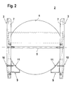
- the webs 7 are from the substantially flat inside of the side part 3 protrude vertically and have a constant height over its length (FIG. 2).
- the cross section the webs 7 is also constant over its length. As can be seen from FIG. 3, the cross section of the webs 7 essentially triangular and tapers continuously to the front end of the web 7.
- the webs 7 are over the entire width of the side part 3 evenly distributed, with the first and last web 7 is formed by a widened wall element, which the side part 3 limited to the respective edge.
- the webs 7 on the side parts 3 are each identical, so that there is a web 7 of the first in pairs Side part 3 and a web 7 of the second side part 3 face.
- the support member 9 is preferably made of Teflon and is with its flat back on the Fixed inside of the side part 3 by means of screws 10.
- the support parts 9 on both side parts 3 are identical and in the same way on the respective side part 3 mounted so that they are opposite each other at the same height are arranged.
- Each support member 9 extends in the longitudinal direction over the entire width of the respective side part 3 and has one constant cross-section over its entire length.
- the level The underside of the support part 9 runs in the horizontal direction.
- the upper edge of the support part 9 runs horizontally Direction and immediately connects to the lower one Edges of the webs 7.
- the top facing the interior of the metal tray 2 of the support member 9 has a support surface 11 which is connected to the Edge contour of the wafer 1 is adapted so that the wafer 1 with a part of its edge lie flush on the bearing surface 11.
- the contact surface 11 has a segment of a circle Cross-section, the radius of curvature of the segment of a circle corresponds to the radius of the wafer 1.
- the number is across the width of the side part 3 distributed webs 7 selected so that a total of 13 Inserts of the same width to accommodate bent wafers 1 arise.
- containers are used in the semiconductor manufacturing plant used, which are essentially identical to the metal trays 2 according to FIGS. 1-3. The only difference refer to the containers according to FIGS. 1-3 Containers double the number of webs 7 so that the The number of slots instead of 13 is now 25. Corresponding the widths of the slots are reduced by half. These containers are used to store non-bent wafers 1 used.
Landscapes
- Packaging Frangible Articles (AREA)
- Container, Conveyance, Adherence, Positioning, Of Wafer (AREA)
Abstract
Description
- Figur 1:
- Perspektivische Darstellung eines Ausführungsbeispiels des erfindungsgemäßen Behälters zum Transport von Wafern.
- Figur 2:
- Längsschnitt durch den Behälter gemäß Figur 1.
- Figur 3:
- Querschnitt durch den Behälter gemäß Figur 1.
- (1)
- Wafer
- (2)
- Metallhorde
- (3)
- Seitenteil
- (4)
- Griff
- (5)
- Distanzstange
- (6)
- Rückenblech
- (7)
- Steg
- (8)
- Stoßstange
- (9)
- Stützteil
- (10)
- Schrauben
- (11)
- Auflagefläche
Claims (18)
- Verfahren zum Transport von als 200 mm - Wafern ausgebildeten Wafern mittels erster Behälter mit einer Kapazität zur Lagerung eines Loses von 25 Wafern, wobei jeder Wafer einzeln in einem Einschub vorgegebener Breite gelagert ist, dadurch gekennzeichnet, dass zur Aufnahme von verbogenen Wafern (1) zweite Behälter mit einer Kapazität zur Lagerung eines Loses von 13 Wafern (1) vorgesehen sind, wobei die Breiten der Einschübe gegenüber den Breiten der Einschübe des ersten Behälters bei gleichen Außenabmessungen beider Behälter vergrößert sind.
- Verfahren nach Anspruch 1, dadurch gekennzeichnet, dass in den ersten Behältern ausschließlich nicht verbogene Wafer (1) und in den zweiten Behältern ausschließlich verbogene Wafer (1) gelagert werden.
- Verfahren nach einem der Ansprüche 1 oder 2, dadurch gekennzeichnet, dass die Breiten der Einschübe der zweiten Behälter doppelt so groß wie die Breiten der Einschübe der ersten Behälter sind.
- Verfahren nach Anspruch 3, dadurch gekennzeichnet, dass die Einschübe von an gegenüberliegenden Seitenwänden der Behälter äquidistant angeordneten Stegen (7) seitlich begrenzt werden, wobei gegenüber der Anordnung der Stege (7) des ersten Behälters bei dem zweiten Behälter jeweils jeder zweite Steg (7) weggelassen wird.
- Behälter zur Aufnahme von als 200 mm - Wafer ausgebildeten Wafern, insbesondere zur Durchführung des Verfahrens nach einem der Ansprüche 1 - 4, dadurch gekennzeichnet, dass dieser Einschübe zur Aufnahme eines Loses von 13 verbogenen Wafern (1) aufweist, wobei die Breiten der Einschübe an die Durchbiegungen der Wafer (1) angepasst sind.
- Behälter nach Anspruch 5, dadurch gekennzeichnet, dass dieser zwei gegenüberliegend angeordnete Seitenteile (3) aufweist, von deren Innenseiten vertikal verlaufende, in Abstand zueinander angeordnete Stege (7) hervorstehen, wobei jeweils ein Steg (7) an einem Seitenteil (3) einem entsprechenden Steg (7) am zweiten Seitenteil (3) gegenüberliegt, und dass ein Einschub zur Lagerung eines Wafers (1) von einem Zwischenraum zwischen benachbarten Stegen (7) eines Seitenteils (3) und des gegenüberliegenden Zwischenraums am anderen Seitenteil (3) gebildet ist.
- Behälter nach Anspruch 6, dadurch gekennzeichnet, dass die Stege (7) an jedem Seitenteil (3) äquidistant angeordnet sind.
- Behälter nach einem der Ansprüche 6 oder 7, dadurch gekennzeichnet, dass sich die Einschübe über nahezu die gesamte Breite der Seitenteile (3) erstrecken.
- Behälter nach einem der Ansprüche 6 - 8, dadurch gekennzeichnet, dass die Zwischenräume zwischen den Stegen (7) am oberen Rand des jeweiligen Seitenteils (3) ausmünden.
- Behälter nach Anspruch 9, dadurch gekennzeichnet, dass die oberen Ränder der Seitenteile (3) mit einer Stoßstange (8) abschließen.
- Behälter nach Anspruch 10, dadurch gekennzeichnet, dass die Stoßstange (8) aus Teflon besteht.
- Behälter nach einem der Ansprüche 6 - 11, dadurch gekennzeichnet, dass die unteren Ränder der Stege (7) eines Seitenteils (3) an ein Stützteil (9) anschließen, wobei jedes Stützteil (9) eine an die Randkontur der Wafer (1) angepasste Auflagefläche (11) aufweist, auf welcher die Wafer (1) abschnittsweise aufliegen.
- Behälter nach Anspruch 12, dadurch gekennzeichnet, dass die Auflagefläche (11) unprofiliert ist.
- Behälter nach einem der Ansprüche 12 oder 13, dadurch gekennzeichnet, dass die Auflagefläche (11) einen kreissegmentförmigen Querschnitt aufweist, wobei der Krümmungsradius des Kreissegments dem Radius eines Wafers (1) entspricht.
- Behälter nach einem der Ansprüche 12 - 14, dadurch gekennzeichnet, dass sich das Stützteil (9) über die gesamte Breite des Seitenteils (3) erstreckt und an diesem befestigt ist.
- Behälter nach einem der Ansprüche 12 - 15, dadurch gekennzeichnet, dass die Stützteile (9) an den beiden Seitenteilen (3) identisch ausgebildet und in Abstand gegenüberliegend angeordnet sind.
- Behälter nach einem der Ansprüche 12 - 16, dadurch gekennzeichnet, dass die Stützteile (9) aus Teflon bestehen.
- Behälter nach eine der Ansprüche 6 - 17, dadurch gekennzeichnet, dass die Seitenteile (3) aus mit Teflon beschichtetem Aluminium bestehen.
Applications Claiming Priority (2)
| Application Number | Priority Date | Filing Date | Title |
|---|---|---|---|
| DE10046942A DE10046942A1 (de) | 2000-09-21 | 2000-09-21 | Verfahren zum Transport von Wafern |
| DE10046942 | 2000-09-21 |
Publications (1)
| Publication Number | Publication Date |
|---|---|
| EP1193737A1 true EP1193737A1 (de) | 2002-04-03 |
Family
ID=7657198
Family Applications (1)
| Application Number | Title | Priority Date | Filing Date |
|---|---|---|---|
| EP01121469A Withdrawn EP1193737A1 (de) | 2000-09-21 | 2001-09-07 | Verfahren zum Transport von Wafern |
Country Status (2)
| Country | Link |
|---|---|
| EP (1) | EP1193737A1 (de) |
| DE (1) | DE10046942A1 (de) |
Cited By (4)
| Publication number | Priority date | Publication date | Assignee | Title |
|---|---|---|---|---|
| WO2013127834A1 (en) | 2012-02-28 | 2013-09-06 | Ge Healthcare As | Vial with free float valve for sterile pharmaceutical |
| CN103693301A (zh) * | 2013-12-17 | 2014-04-02 | 徐玉文 | 一种弧形锅巴固定器 |
| CN104299937A (zh) * | 2013-07-15 | 2015-01-21 | 北大方正集团有限公司 | 一种应用于硅腐蚀的固定装置 |
| CN112670218A (zh) * | 2019-10-16 | 2021-04-16 | 沈阳芯源微电子设备股份有限公司 | 一种兼容式半导体晶圆浸泡片盒装置 |
Citations (6)
| Publication number | Priority date | Publication date | Assignee | Title |
|---|---|---|---|---|
| US4767002A (en) * | 1986-01-14 | 1988-08-30 | W. R. Grace & Co. | Multiple circuit board carrier/shipper |
| US5725101A (en) * | 1995-06-26 | 1998-03-10 | Kakizaki Manufacturing Co., Ltd. | Thin-plate supporting container |
| US5988393A (en) * | 1998-06-15 | 1999-11-23 | United Microelectronics Corp. | Storage box for semiconductor wafers |
| DE19924182A1 (de) * | 1998-05-28 | 1999-12-02 | Fluoroware Inc | Träger für zu bearbeitende, aufzubewahrende und/oder zu transportierende Scheiben |
| US6079927A (en) * | 1998-04-22 | 2000-06-27 | Varian Semiconductor Equipment Associates, Inc. | Automated wafer buffer for use with wafer processing equipment |
| EP1148536A2 (de) * | 2000-04-17 | 2001-10-24 | Shin-Etsu Polymer Co., Ltd. | Tragevorrichtung für einen Wafertransportbehälter |
Family Cites Families (2)
| Publication number | Priority date | Publication date | Assignee | Title |
|---|---|---|---|---|
| JP2791971B2 (ja) * | 1994-06-17 | 1998-08-27 | 信越ポリマー株式会社 | ウェーハ収納容器におけるウェーハバスケット |
| US5853214A (en) * | 1995-11-27 | 1998-12-29 | Progressive System Technologies, Inc. | Aligner for a substrate carrier |
-
2000
- 2000-09-21 DE DE10046942A patent/DE10046942A1/de not_active Withdrawn
-
2001
- 2001-09-07 EP EP01121469A patent/EP1193737A1/de not_active Withdrawn
Patent Citations (6)
| Publication number | Priority date | Publication date | Assignee | Title |
|---|---|---|---|---|
| US4767002A (en) * | 1986-01-14 | 1988-08-30 | W. R. Grace & Co. | Multiple circuit board carrier/shipper |
| US5725101A (en) * | 1995-06-26 | 1998-03-10 | Kakizaki Manufacturing Co., Ltd. | Thin-plate supporting container |
| US6079927A (en) * | 1998-04-22 | 2000-06-27 | Varian Semiconductor Equipment Associates, Inc. | Automated wafer buffer for use with wafer processing equipment |
| DE19924182A1 (de) * | 1998-05-28 | 1999-12-02 | Fluoroware Inc | Träger für zu bearbeitende, aufzubewahrende und/oder zu transportierende Scheiben |
| US5988393A (en) * | 1998-06-15 | 1999-11-23 | United Microelectronics Corp. | Storage box for semiconductor wafers |
| EP1148536A2 (de) * | 2000-04-17 | 2001-10-24 | Shin-Etsu Polymer Co., Ltd. | Tragevorrichtung für einen Wafertransportbehälter |
Cited By (5)
| Publication number | Priority date | Publication date | Assignee | Title |
|---|---|---|---|---|
| WO2013127834A1 (en) | 2012-02-28 | 2013-09-06 | Ge Healthcare As | Vial with free float valve for sterile pharmaceutical |
| CN104299937A (zh) * | 2013-07-15 | 2015-01-21 | 北大方正集团有限公司 | 一种应用于硅腐蚀的固定装置 |
| CN104299937B (zh) * | 2013-07-15 | 2017-11-21 | 北大方正集团有限公司 | 一种应用于硅腐蚀的固定装置 |
| CN103693301A (zh) * | 2013-12-17 | 2014-04-02 | 徐玉文 | 一种弧形锅巴固定器 |
| CN112670218A (zh) * | 2019-10-16 | 2021-04-16 | 沈阳芯源微电子设备股份有限公司 | 一种兼容式半导体晶圆浸泡片盒装置 |
Also Published As
| Publication number | Publication date |
|---|---|
| DE10046942A1 (de) | 2002-04-25 |
Similar Documents
| Publication | Publication Date | Title |
|---|---|---|
| DE102011051857B3 (de) | Warenvorschubeinsatz für ein Warenvorschubsystem | |
| EP0734974A1 (de) | Lagerregal | |
| EP1193737A1 (de) | Verfahren zum Transport von Wafern | |
| EP3420857B1 (de) | Aufstellraum zum kühlen oder tiefkühlen von waren mit einem regalsystem | |
| EP0281955B1 (de) | Langmateriallagereinrichtung | |
| DE2719763A1 (de) | Schaugestell fuer waren | |
| EP0634334B1 (de) | Lagerbehälter mit Führungselementen | |
| EP4461671A1 (de) | Regalanordnung | |
| DE102017116721B4 (de) | Lagereinrichtung für Coils oder Bandringe aller Art | |
| DE3728296A1 (de) | Werkstuecktraeger-gestell | |
| EP0614794B1 (de) | Transportgestell | |
| AT521925B1 (de) | Substratkassette | |
| EP3715008B1 (de) | Stabfördervorrichtung zum fördern von metallstäben | |
| EP3095736A2 (de) | Förderstrecke einer anzahl von mit traversen gekoppelten bandunterstützungmodulen | |
| DE4142355A1 (de) | Verfahrbare krananlage | |
| WO1981002877A1 (fr) | Installation pour l'entreposage et le transport d'objets allonges | |
| DE69206475T2 (de) | Bodenrahmen für elektrischen Kasten. | |
| EP4638309A1 (de) | Lagergutträger-einsatz, lagergutträger und lagerregal | |
| DE202025105992U1 (de) | Rollbehälter | |
| DE9303527U1 (de) | Durchlaufregal, insbesondere für Kommissionierzwecke | |
| DE29807208U1 (de) | Hochregal | |
| EP4403491A1 (de) | Regalsystemverbinder | |
| DE102022100176A1 (de) | Leitsegement, Geländer zur Fördermittelflankierung, Lebensmittelbehälter-Förderanlage, Computerprogrammprodukt und Lebensmittelbehälter-Förderverfahren | |
| DE202025001800U1 (de) | Ladenbaugitter | |
| DE9301050U1 (de) | Ständer für Compact-Disks |
Legal Events
| Date | Code | Title | Description |
|---|---|---|---|
| PUAI | Public reference made under article 153(3) epc to a published international application that has entered the european phase |
Free format text: ORIGINAL CODE: 0009012 |
|
| AK | Designated contracting states |
Kind code of ref document: A1 Designated state(s): AT BE CH CY DE DK ES FI FR GB GR IE IT LI LU MC NL PT SE TR Kind code of ref document: A1 Designated state(s): AT DE FR GB IT |
|
| AX | Request for extension of the european patent |
Free format text: AL;LT;LV;MK;RO;SI |
|
| 17P | Request for examination filed |
Effective date: 20020425 |
|
| AKX | Designation fees paid |
Free format text: AT DE FR GB IT |
|
| 17Q | First examination report despatched |
Effective date: 20041208 |
|
| 17Q | First examination report despatched |
Effective date: 20041208 |
|
| GRAP | Despatch of communication of intention to grant a patent |
Free format text: ORIGINAL CODE: EPIDOSNIGR1 |
|
| STAA | Information on the status of an ep patent application or granted ep patent |
Free format text: STATUS: THE APPLICATION IS DEEMED TO BE WITHDRAWN |
|
| 18D | Application deemed to be withdrawn |
Effective date: 20081205 |