EP1193552A2 - Verfahren zum Erzeugen von Masken-Layot-Daten für die Lithografiesimulation und von optimierten Masken-Layout-Daten sowie zugehörige Vorrichtung und Programme - Google Patents
Verfahren zum Erzeugen von Masken-Layot-Daten für die Lithografiesimulation und von optimierten Masken-Layout-Daten sowie zugehörige Vorrichtung und Programme Download PDFInfo
- Publication number
- EP1193552A2 EP1193552A2 EP01118800A EP01118800A EP1193552A2 EP 1193552 A2 EP1193552 A2 EP 1193552A2 EP 01118800 A EP01118800 A EP 01118800A EP 01118800 A EP01118800 A EP 01118800A EP 1193552 A2 EP1193552 A2 EP 1193552A2
- Authority
- EP
- European Patent Office
- Prior art keywords
- layout
- data
- mask
- original
- new
- Prior art date
- Legal status (The legal status is an assumption and is not a legal conclusion. Google has not performed a legal analysis and makes no representation as to the accuracy of the status listed.)
- Granted
Links
Images



Classifications
-
- G—PHYSICS
- G03—PHOTOGRAPHY; CINEMATOGRAPHY; ANALOGOUS TECHNIQUES USING WAVES OTHER THAN OPTICAL WAVES; ELECTROGRAPHY; HOLOGRAPHY
- G03F—PHOTOMECHANICAL PRODUCTION OF TEXTURED OR PATTERNED SURFACES, e.g. FOR PRINTING, FOR PROCESSING OF SEMICONDUCTOR DEVICES; MATERIALS THEREFOR; ORIGINALS THEREFOR; APPARATUS SPECIALLY ADAPTED THEREFOR
- G03F1/00—Originals for photomechanical production of textured or patterned surfaces, e.g., masks, photo-masks, reticles; Mask blanks or pellicles therefor; Containers specially adapted therefor; Preparation thereof
- G03F1/36—Masks having proximity correction features; Preparation thereof, e.g. optical proximity correction [OPC] design processes
-
- H—ELECTRICITY
- H10—SEMICONDUCTOR DEVICES; ELECTRIC SOLID-STATE DEVICES NOT OTHERWISE PROVIDED FOR
- H10P—GENERIC PROCESSES OR APPARATUS FOR THE MANUFACTURE OR TREATMENT OF DEVICES COVERED BY CLASS H10
- H10P74/00—Testing or measuring during manufacture or treatment of wafers, substrates or devices
-
- G—PHYSICS
- G03—PHOTOGRAPHY; CINEMATOGRAPHY; ANALOGOUS TECHNIQUES USING WAVES OTHER THAN OPTICAL WAVES; ELECTROGRAPHY; HOLOGRAPHY
- G03F—PHOTOMECHANICAL PRODUCTION OF TEXTURED OR PATTERNED SURFACES, e.g. FOR PRINTING, FOR PROCESSING OF SEMICONDUCTOR DEVICES; MATERIALS THEREFOR; ORIGINALS THEREFOR; APPARATUS SPECIALLY ADAPTED THEREFOR
- G03F7/00—Photomechanical, e.g. photolithographic, production of textured or patterned surfaces, e.g. printing surfaces; Materials therefor, e.g. comprising photoresists; Apparatus specially adapted therefor
- G03F7/70—Microphotolithographic exposure; Apparatus therefor
- G03F7/70425—Imaging strategies, e.g. for increasing throughput or resolution, printing product fields larger than the image field or compensating lithography- or non-lithography errors, e.g. proximity correction, mix-and-match, stitching or double patterning
- G03F7/70433—Layout for increasing efficiency or for compensating imaging errors, e.g. layout of exposure fields for reducing focus errors; Use of mask features for increasing efficiency or for compensating imaging errors
-
- G—PHYSICS
- G03—PHOTOGRAPHY; CINEMATOGRAPHY; ANALOGOUS TECHNIQUES USING WAVES OTHER THAN OPTICAL WAVES; ELECTROGRAPHY; HOLOGRAPHY
- G03F—PHOTOMECHANICAL PRODUCTION OF TEXTURED OR PATTERNED SURFACES, e.g. FOR PRINTING, FOR PROCESSING OF SEMICONDUCTOR DEVICES; MATERIALS THEREFOR; ORIGINALS THEREFOR; APPARATUS SPECIALLY ADAPTED THEREFOR
- G03F7/00—Photomechanical, e.g. photolithographic, production of textured or patterned surfaces, e.g. printing surfaces; Materials therefor, e.g. comprising photoresists; Apparatus specially adapted therefor
- G03F7/70—Microphotolithographic exposure; Apparatus therefor
- G03F7/70483—Information management; Active and passive control; Testing; Wafer monitoring, e.g. pattern monitoring
- G03F7/70491—Information management, e.g. software; Active and passive control, e.g. details of controlling exposure processes or exposure tool monitoring processes
- G03F7/705—Modelling or simulating from physical phenomena up to complete wafer processes or whole workflow in wafer productions
Definitions
- the invention relates to a method for generating mask layout data for the simulation of a lithography process
- Original data is specified, which is an original laycut establish.
- Based on the origin data will be automatic calculated new data.
- the calculation is done in such a way that a new mask layout defined by the new data in terms of geometry one with the original data manufacturable or manufactured mask similar to that Original layout is.
- an associated device and an associated program are associated with the new layout with reduced effort.
- the invention is based on the knowledge that deviations a mask defined by a layout from one to the other this layout produced or one based on this Modeled the layout by emulating the manufacturing process Mask due to the manufacturing process. These deviations depend on the geometry of the ones to be manufactured Mask off and can already be due to the geometry largely determine the original layout. This makes possible it, a replica of the individual steps of the manufacturing process to avoid and yet the influences of Manufacturing process on the geometry quickly and without big effort to consider.
- the to be used for the lithography simulation calculated on the basis of rules based on deviations in the Geometry of a layout from one made according to this layout Mask based.
- the mask used for comparison also based on the Layout simulating the steps of the manufacturing process model. In both. Cases are with the invention Process the individual process steps of the manufacturing process the mask when calculating the new data but not replicated. Entering a variety of Process parameters for the replication of the manufacturing process and the computationally complex replication itself is eliminated in order to.
- the deviations in the geometry can be solved by simple calculate geometric relationships. Differential equations, such as. Diffusion equations cannot be solved. This allows the new mask data to be saved with an im Comparison to replicate the manufacturing process by orders of magnitude calculate reduced computing effort.
- the rules to determine geometric calculation rules the limits of a structure at a position in the new layout depending on the length and / or area of one on the same position in the original layout reference structure. Alternatively or cumulatively, the distance of the Reference structure to the neighboring structures of the original layout included in the calculation rule. The length and the area of a structure determine the size of the one to be determined Deviations.
- the neighboring structures allow Conclusions about where deviations occur become. During the mask writing process from closely neighboring Structures have different effects than when writing neighboring structures with larger ones Distance to the reference structure.
- a shortening value becomes according to a rule for an elongated reference structure, which too is referred to as a line structure or in short as a line a position of the original layout.
- a line structure or in short as a line a position of the original layout.
- the line shortening leaves attributed to the lack of neighboring structures.
- the type of line shortening and the degree of line shortening can be determined based on the geometry of the original layout. Line shortenings are shown in Figures 2 to 4, which are explained in more detail.
- an angular reference structure at a position in the original layout ermictelt.
- a corner can be created using the Angle between two lines or define straight edges.
- the structures have one usual design often corners, the edges of which are at an angle of 90 ° to each other (but there are also any angles conceivable).
- To round a corner at least one radius or curvature value determined or by an operator entered.
- the new data is calculated so that it is in the same position Structure in the new layout instead of the corner has a rounded edge.
- the radius value leaves for example directly from the width of a structure determine.
- You can then lay out the circular equation, for example use. Corner roundings are shown below using the figures 2 to 5 explained.
- the radius becomes dependent on the environment selected.
- a light absorbing structure that is around a translucent structure is arranged around a inside corner rounded with a smaller radius, as an outside corner of the light absorbing structure.
- a position of the origin layout determined.
- the narrowing value will then be at the same position in the new layout structure compared to the reference structure narrowed at least in sections transversely to the longitudinal direction. This measure creates the so-called "peanuts" effect taken into account, because narrowing of structures is reproduced be due to the lack of neighboring structures during the manufacture of the mask.
- the invention in a second aspect, relates to a method for generating optimized mask layout data for photo masks.
- Original data specified which is an original layout for the Define simulation of a lithography process. outgoing from the original data are automatically or otherwise and way new data is calculated.
- the new data insert new layout, the one with the geometry the mask produced or producible from the original data is more similar to the original layout.
- the new data can be reproduced of the procedural steps in making the mask.
- the method according to the first can also be used Aspect or according to one of the training and Use configurations to define the new data.
- the invention according to the second aspect is based on the consideration out that taking into account the influence of the manufacturing process the mask is only a partial step on the way to That is, setting final mask layout data actually used for mask making.
- the changes occurring during the manufacturing process for their part require a change in the original layout in a corrected layout.
- the inventive method according to the second aspect data automatically corrected based on the new data set so that one made with the corrected data or producible corrected mask with regard to the Geometry more similar to the original layout than one with the Original data is manufactured or manufacturable mask.
- the original layout becomes the goal of the manufacturing process looking at the mask.
- the reference to the original layout allows simple criteria for the automatic correction.
- the corrected data set so that the with the corrected data manufactured or producible mask better lithographic imaging properties than one with has the mask produced or producible from the original data.
- the lithographic imaging properties are for the achievable structure widths in the wafer exposure of fundamental importance.
- One criterion for automatic correction is one Further training the relationship of the dark areas and the bright areas of the original layout. In the corrected layout this ratio should be maintained or by a predetermined one Value to be changed.
- the area ratio is namely initially in the new layout based on the considered Effects changed.
- the corrected layout data calculated based on correction rules based on deviations in the geometry of a layout from one made according to this layout or one based on this layout below Replica of the manufacturing process modeled mask based.
- Geometry can already define so many correction rules that the correction is complete or almost complete can be automated.
- the above in connection with the Shortened value addressed methods for determining the new data. Then according to a correction rule depending on the shortening value for a reference structure on a Position of the original layout determines an extension value. Depending on the renewal value, the in the same position in the corrected layout Structure compared to that in the same position in the new layout lying structure extended in the longitudinal direction. The aim here is to be based on the original layout Approach structure in the same position. This takes place, for example, in an iteration process. however approximation rules can also be used. A correction process is explained below with reference to FIG. 8.
- the one mentioned above is discussed Procedure related to the radius or curvature value used.
- an extension value at a position of the original layout certainly.
- the renewal value is then those in the same position in the corrected layout lying structure compared to that in the same position Longitudinal structure in the new layout and / or extended in the transverse direction. With this configuration shortenings are caused by the rounding of the corners be balanced again.
- the extension and / or the broadening is in a further education while maintaining the shape of the structure in the new mask.
- the Also extend or widen simple structures. For example, if you want to correct rounding, so small squares become left and right of a central axis attached to the structure of the original mask to the corrected Maintain structure. The structure thus receives one serif-shaped shape, as used by.
- OPC method is known (Optical Proximity Correction - correction of neighborhood-induced Diffraction effects).
- Known OPC processes take into account the exposure process in particular of the wafer.
- the method according to the invention essentially takes into account the effects caused by the Mask writer and the mask manufacturing process evoked become.
- the invention also relates to a device, in particular a data processing system for generating mask layout data for lithography simulation or generation optimized mask layout data for photo masks.
- a device in particular a data processing system for generating mask layout data for lithography simulation or generation optimized mask layout data for photo masks.
- circuit arrangements or a Special hardware in a data processing system used
- the device is designed so that the method steps during operation according to one of the methods according to the first aspect or according to the second aspect or according to their further developments be carried out. So the above technicals apply Effects also for the device.
- the invention relates to a program with a a data processing system executable command sequence.
- the command sequence will be the procedural steps according to the first aspect or according to the second aspect or according to advanced training on one of these aspects.
- the program is located in a RAM module, for example (Random Access Memory), in a programmable memory chip, on a floppy disk or on a compact disc, in short Called CD.
- FIG. 1 shows a basic illustration of wafer lithography and the lithography simulation as well as the process steps to generate the layout data for a during manufacturing Photo mask used by integrated circuits.
- the data format is for input into a program for simulation of the lithography process based on the original layout data suitable.
- Such programs are, for example the "Solid-C” program from Sigma-C or the program "Prolith” from Finle.
- the data 12 becomes, for example by an upstream development department depending on the electrical properties of the circuit.
- One in an ideal manufacturing process according to the original layout 10 manufactured integrated circuit would thus meet the electrical requirements.
- join a real manufacturing process as early as the manufacturing stage a mask based on the original layout 10 deviations on.
- the original layout 10 contains three rectangular dark ones Structures 14, 16 and 18.
- An arrow 20 symbolizes the Manufacturing process of a mask based on the original layout data 12 of the original mask 10.
- One is created Mask 22 with three dark structures 24, 26 and 28, their Width each e.g. Is 100 manometers.
- the structures 24, 26 and 28 are in this order in the mask 22 on the same position as structures 14, 16 and 18 in the Source layout 10.
- As a reference point for example the top left corner 30 of the original layout 10 and Use upper left corner 32 of mask 22.
- the Deviations calculated based on the given rules The Regein take into account the extent and area of the respective machined structure 14, 16 and 18 and the Influence of neighboring structures 16 to 18.
- Result of the execution of the geometry change process are layout data of a new mask layout 42, the dark one Contains structures 44, 46 and 48 in that order correspond to structures 14, 16 and 15.
- “Correspond” in this context means that a structure in the Source layout 10 is in the same position as that corresponding structure in the new mask layout 42.
- Die Structures 44, 46 and 48 have rounded ones, for example Corners and are compared to structures 14, 16 and 18, respectively shortened. This shortening of the lines is shown below using the figure 2 to 4 explained in more detail. Structures 44, 46 and 48 have structures 24, 26 and 28 of mask 22 very similar To form.
- the new mask layout 42 manually corrected to meet the requirements of the upstream Development department, cf. arrows 50 and 52. Corrected layout data are then used instead of the layout data 12 of the original layout 10. By simple or multiple iteration arises instead of the new mask layout 42 one or more new ones Mask layout.
- the data of the last new mask layout are used for the simulation of exposure and development be used when processing a wafer, see Arrow 54 and process step 56. For example, for simulation one of the already mentioned program "Solid-C" and "Prolith" used.
- the Exposure process 60 would with an exposure device 62 are carried out at the time of simulation 56 can still be in the development stage. In this case are instead of actual parameters as development goals enter the set parameters.
- the exposure device 62 contains, for example, a laser unit 64 for generating a laser beam 66 that the structures on the mask by means of an optic, usually reduced to one silicon wafer 72 coated with a photoresist layer 70 (Wafer).
- the method steps the exposure process 60 and the development process of the photoresist is reproduced using calculations with the help of equations that are running describe physical processes.
- result data 74 are output, see arrow 76.
- the result data represent a paint sample, which essentially corresponds to a lacquer pattern 78, such as it with the help of the exposure device 62 and the development process could actually be made, see Arrow 80.
- a lacquer pattern 78 such as it with the help of the exposure device 62 and the development process could actually be made, see Arrow 80.
- On the silicon wafer 72 are elongated Photoresist structures 82, 84 and 86 remained in this Order corresponds to structures 14, 16 and 18.
- result data 74 further corrections are often made layout data required, see arrows 88 and 52.
- result data generated for the simulation of further process steps suitable in the manufacture of an integrated circuit are, see arrow 90. For example, then Etching of silicon wafer 72 simulated.
- Figure 2 shows the effects "line shortening” and "corner rounding" using structures 100, 102 and 104 of an original layout 110 and corresponding to these structures Structures 120, 122 and 124 of a new mask layout 130.
- Points 132 and 134 illustrate that the structures shown 100, 102 and 104 above and below further parallel Connect structures.
- Points 136 and 138 illustrate the same situation for structures 120, 122 and 124.
- That new mask layout 130 was created using the geometry change method 34 from the layout data of the original layout 110 generated, influences the manufacturing process have been taken into account for real masks. Thus resembles the new mask layout 130 one using the original layout 110 manufactured mask.
- Lines 140, 142 and 144 show the original in the new mask layout 130 Course of structures 100, 102 and 104.
- the line shortening is parallel for the three in the Structures 120, 122 and 124 arranged at the same distance same, so in the following only the shortening and the Corner rounding for structure 122 is explained.
- the Structure 122 is on one side compared to structure 102 End shortened by a difference value D1, which is a distance 150 corresponds.
- Figure 3 shows the effect of an increased "line shortening" at the edge of a structure of an original layout 170 in comparison to a new mask layout 190.
- the effect turns on Hand of structures 160, 162 and 164 of the original layout 170 and structures 180, 182 corresponding to these structures and 184 of the new mask layout 190.
- Points 192 clarify that the structures 160, 162 shown and 164 connect further parallel structures downwards.
- Points 194 illustrate the same situation for the Structures 180, 182 and 184. Closing upwards no structures on structures 160, 162 and 164 or 180, 182 and 184.
- the new mask layout 190 was used of the geometry change method 34 from the layout data of the original layout 170, with influences of the Manufacturing process for real masks has been taken into account are. Thus, the new mask layout 190 resembles one with the help of the original layout 170 mask.
- Lines 200, 202 and 204 show the original in the new mask layout 190 Course of structures 100, 102 and 104.
- the line shortening is greatest for structure 180.
- the structure 182 and 184 is in Compare to structure 162 or 164 at one end shortens a difference value D2, which is a distance 210 equivalent.
- the difference value D2 has approximately the same value like the difference value D1.
- the structure 180 is in Compared to structure 160 shortened by a difference value, which is greater than the difference value D3, see route D3.
- FIG. 4 shows the effect of a reduced "line shortening" due to an adjacent structure 360 or 362 Hand of structures 300, 302 and 304 of an original layout 310 and structures 320, 322 corresponding to these structures and 324 a new mask layout 330.
- Points 332 and 334 clarify that the structures 300, 302 shown and 304 connect further parallel structures above and below.
- Points 336 and 338 illustrate the same facts for structures 320, 322 and 324.
- Structure 360 lies across the structures 300, 302 and 304 at a distance from the Start of these structures, the distance between neighboring structures 300, 302 and 304 corresponds.
- Structure 362 lies across the structures 320, 322 and 324 at a distance from the Start of these structures, the distance between neighboring structures 320, 322 and 324.
- the new mask layout 330 was created using the geometry change method 34 from the layout data of the original layout 310 generated, influences the manufacturing process have been taken into account for real masks.
- the new mask layout 330 thus resembles one using the Source layouts 310 made mask.
- Lines 340, 342 and 344 in the new mask layout 330 show the original Course of structures 300, 302 and 304.
- the line shortening is parallel for the three in the Structures 120, 122 and 124 arranged at the same distance same, so in the following only the shortening and the Corner rounding for structure 322 is explained.
- the Structure 322 is on one side compared to structure 302 End shortened by a difference value D4, which is a distance 350 corresponds.
- Figure 5 shows the effect of "corner rounding" on irregular modified structures 400 to 406 of an original layout 410 compared to structures 420 to 426 one new layouts 430 using the geometry change method 34 has been calculated.
- the structures 400 to 406 have so-called serifs at the corners, see e.g. a Serif 440.
- the Sarlfan were subjected to an OPC procedure originally added rectangular structures. In the structures 420 to 426 there are roundings in the area of the corners.
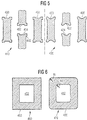
- Figure 6 shows the effect of "corner rounding" in a dark structure 450, which is a bright rectangular light Structure 452 surrounds. Both structures belong to an original layout 460. With the help of the original layout of the geometry change method 34 a new mask layout 470 calculates that corresponding to structures 450 and 452, respectively Contains structures 480 and 482, respectively. The outer corners of the dark Structure 480 are rounded with a radius R1 that is larger than a radius R2 with which the inner corners the structure 480 are rounded.
- Figure 7 shows the so-called "peanuts" effect using rectangular structures 490 to 496 of an original layout 500 compared to structures 510 to 516 one new mask layouts 520, using the geometry change method 34 calculated from the original layout 500 has been.
- the structures 510 to 516 are in central sections Restricted, see e.g. Narrowing 522, The Narrowing are due to the lack of closely adjacent structures.
- FIG. 8 shows an original layout 600 and a new mask layout 602, whose mask data by iterative application of the Geometry change method 34 have been calculated. at this calculation was first the change of structures the original layout 600, e.g. structure 604 of the manufacturing process. The changes resulted to a first new mask layout (not shown). Then the layout data was started from the first corrected new mask layout. The new mask layout 602 was then carried out again by performing the geometry change procedure 34 from the corrected layout data.
- the layout data was corrected so that the areas of dark structures 604 and 606 are the same. This is possible if the curves of structure 606 have a Frame 608 stands out, which the original location of the Structure 606 corresponds to structure 204.
- the corrected data are used to manufacture a mask used.
- the corners of the structures in the corrected layout are not rounded.
Landscapes
- Physics & Mathematics (AREA)
- General Physics & Mathematics (AREA)
- Preparing Plates And Mask In Photomechanical Process (AREA)
- Exposure And Positioning Against Photoresist Photosensitive Materials (AREA)
Abstract
Description
- Figur 1
- eine Prinzipdarstellung Wafer-Lithografie und Lithografiesimulation sowie Verfahrensschritte zum Erzeugen der Layout-Daten für eine LithografieMaske,
- Figur 2
- die Effekte "Linienverkürzung" und "Eckenabrundung" an Hand von Strukturen in der Mitte eines Ursprungs-Layouts,
- Figur 3
- den Effekt einer verstärkten "Linienverkürzung" am Rand einer Struktur eines Ursprungs-Layouts,
- Figur 4
- den Effekt einer verringerten "Linienverkürzung" aufgrund einer benachbarten Struktur,
- Figur 5
- den Effekt der "Eckenabrundung" bei unregelmäßig geränderten Strukturen,
- Figur 6
- den Effekt der "Eckenabrundung" bei einer dunklen Struktur, die eine helle Struktur umgibt,
- Figur 7
- den sogenannten "Peanuts"-Effekt, und
- Figur 8
- eine Ursprungs-Maske sowie eine daraus berechnete und bezüglich des Effektes der Linienverkürzung korrigierte Maske.
- Linienverkürzung,
- Einengungen einer langgestreckten Struktur in bestimmten Abschnitten, sogenannter "Peanuts"-Effekt,
- Abrundungen der Ecken, und
- CD-Linearität (Critical Dimension) .
- Linienverkürzungen durch Verlängerung der betreffenden Strukturen beseitigt,
- Abrundungen von Ecken durch "Anstückeln" von Korrekturflächen vermieden, und
- Einengungen aufgrund des "Peanuts"-Effektes wieder verbreitert.
- 10
- Ursprungs-Layout
- 12
- Ursprungs-Layout-Daten
- 14, 16, 18
- dunkle Struktur
- 20
- Herstellungsprozess
- 22
- Maske
- 24, 26, 28
- dunkle Struktur
- 30, 32
- linke obere Ecke
- 34
- Geometrieänderungs-Verfahren
- 36, 38, 40
- Pfeil
- 42
- neues Maske-Layout
- 44, 46, 48
- dunkle Struktur
- 50, 52, 54
- Pfeil
- 56
- Simulation
- 58
- Parameter
- 60
- Belichtungsprozess
- 62
- Belichtungsvorrichtung
- 64
- Lasereinheit
- 66
- Laserstrahl
- 70
- Fotolackschicht
- 72
- Siliziumscheibe
- 74
- Ergebnisdaten
- 76
- Pfeil
- 78
- Lackstrukturen
- 80
- Pfeil
- 82, 84, 86
- Fotolackstruktur
- 88, 90
- Pfeil
- 100, 102, 104
- Struktur
- 110
- Ursprungsmasken-Layout
- 120, 122, 124
- Struktur
- 130
- neues Masken-Layout
- 132 bis 138
- Punkte
- 140, 142, 144
- Linie
- 150
- Strecke
- 152
- Strukturbreite
- 160, 162, 164
- Struktur
- 170
- Ursprungs-Layout
- 180, 182, 184
- Struktur
- 190
- neues Masken-Layout
- 192, 194
- Punkte
- 200, 202, 204
- Linie
- 210
- Strecke
- 212
- Strukturbreite
- 214
- Strecke
- 302, 304, 306
- Struktur
- 310
- Ursprungs-Layout
- 320, 322, 324
- Struktur
- 330
- neues Masken-Layout
- 332 bis 338
- Punkte
- 340, 342, 344
- Linie
- 350
- Strecke
- 352
- Strukturbreite
- 360, 362
- benachbarte Struktur
- 400 bis 406
- Struktur
- 410
- Ursprungs-Layout
- 420 bis 426
- Struktur
- 430
- neues Masken-Layout
- 440
- Serife
- 450
- dunkle Struktur
- 452
- helle Struktur
- 460
- Ursprungs-Layout
- 470
- neues Masken-Layout
- 490 bis 496
- Strecke
- 500
- Ursprungs-Layout
- 510 bis 516
- Struktur
- 520
- neues Masken-Layout
- 522
- Verengung
- 480, 482
- Struktur
- R1, R2
- Radius
- 600
- Ursprungs-Maske
- 602
- neues Masken-Layout
- 604, 606
- Struktur
- 608
- Rahmen
- D1 bis D4
- Differenzwert
Claims (17)
- Verfahren zum Erzeugen von Masken-Layout-Daten für die Lithografiesimulation,dadurch gekennzeichnet, dass die neuen Daten (54) aufgrund von Regeln berechnet werden (34), die auf Abweichungen in der Geometrie eines Layouts von einer nach diesem Layout hergestellten oder einer ausgehend von diesem Layout unter Nachbildung der Schritte des Herstellungsprozesses modellierten Maske beruhen (38, 40).bei dem Ursprungsdaten (12) vorgegeben werden, die ein Ursprungslayout (10) festlegen,automatisch ausgehend von den Ursprungsdaten (12) neue Daten (54) berechnet werden, die eine neues Layout (42) festlegen,und bei dem das neue Layout (42) hinsichtlich der Geometrie einer mit den Ursprungsdaten (12) hergestellten oder herstellbaren Maske (22) ähnlicher als dem Ursprungs-Layout (10) ist,
- Verfahren nach Anspruch 1, dadurch gekennzeichnet, dass die Regeln geometrische Berechnungsvorschriften zum Festlegen der Grenzen einer Struktur an einer Position des neuen Layouts (42) abhängig von der Länge und/oder der Fläche einer an der gleichen Position in dem Ursprungs-Layout (10) liegenden Bezugsstruktur und/oder abhängig vom Abstand der Bezugsstruktur zu benachbarten Strukturen enthalten.
- Verfahren nach Anspruch 1 oder 2, dadurch gekennzeichnet, dass gemäß einer Regel ein Verkürzungswert (150) für eine langgestreckte Bezugsstruktur (102) an einer Position des Ursprungs-Layouts (110) ermittelt wird,
und dass abhängig vom Verkürzungswert (150) die an der gleichen Position in dem neuen Layout (130) liegende Struktur im Vergleich zur Bezugsstruktur (102) in Längsrichtung verkürzt wird. - Verfahren nach einem der vorhergehenden Ansprücha, dadurch gekennzeichnet, dass gemäß einer Regel eine eckige Bezugsstruktur (102) an einer Position des Ursprungs-Layouts (10) ermittelt wird,dass mindestens ein Radius- oder Krümmungswert zum Abrunden einer Ecke ermittelt oder vorgegeben wird,und dass abhängig vom Radius- oder Krümmungswert die an der gleichen Position in dem neuen Layout (130) liegende Struktur anstelle der Ecke einen abgerundeten Kantenverlauf hat.
- Verfahren nach Anspruche 4, dadurch gekennzeichnet, dass bei einer Licht absorbierenden Struktur (430), die um eine Licht durchlässige Struktur (482) herum liegt, eine innere Ecke mit einem kleineren Radius (R2) abgerundet wird als eine äußere Ecke der Licht absorbierenden Struktur (480).
- Verfahren nach einem der vorhergehenden Ansprüche, dadurch gekennzeichnet, dass gemäß einer Regel ein Einengungswert für eine langgestreckte Bezugsstruktur an einer Position des Ursprungs-Layouts ermittelt wird,
und dass abhängig vom Einengungswert die an der gleichen Position in dem neuen Layout liegende Struktur im Vergleich zur Bezugsstruktur zumindest abschnittsweise quer zur Längsrichtung eingeengt wird. - Verfahren zum Erzeugen von optimierten Masken-Layout-Daten für Fotomasken,dadurch gekennzeichnet, dass automatisch ausgehend von den neuen Daten korrigierte Daten eines korrigierten Layouts so festgelegt werden, dass eine mit den korrigierten Daten hergestellte oder herstellbare korrigierte Maske hinsichtlich der Geometrie dem Ursprungs-Layout (10) ähnlicher als einer mit den Ursprungsdaten (12) hergestellten oder herstellbaren Maske (22) ist,bei dem Ursprungsdaten (12) vorgegeben werden, die ein Ursprungs-Layout (10) festlegen,ausgehend von den Ursprungsdaten (12) neue Daten (54) berechnet werden, die ein neues Layout (42) festlegen,und bei dem das neue Layout (42) hinsichtlich der Geometrie einer mit den Ursprungsdaten (12) hergestellten oder herstellbaren Maske (22) ähnlicher als dem Ursprungs-Layout (10) ist,
und/oder, dass die mit den korrigierten Daten hergestellte oder herstellbare korrigierte Maske bessere lithografische Eigenschaften hat, als eine mit den Ursprungsdaten hergestellte oder herstellbare Maske. - Verfahren nach Anspruch 7, dadurch gekennzeichnet, dass zum Ermitteln der neuen Daten (54) ein Verfahren nach einem der Ansprüche 1 bis 7 ausgeführt wird.
- Verfahren nach Anspruch 7 oder 8, dadurch gekennzeichnet, dass das Verhältnis der dunklen Flächen und der hellen Flächen des Ursprungs-Layouts im korrigierten Layout erhalten bleibt oder um einen vorgegebenen Wert geändert wird.
- Verfahren nach einem der Ansprüche 7 bis 9, dadurch gekennzeichnet, dass die korrigierten Daten (54) aufgrund von Korrekturregeln berechnet werden (34), die auf Abweichungen in der Geometrie eines Layouts von einer nach diesem Layout-hergestellten oder einer ausgehend von diesem Layout unter Nachbildung des Herstellungsprozesses modellierten Maske beruhen (38, 40).
- Verfahren nach Anspruch 10 und 3, dadurch gekennzeichnet, dass gemäß einer Korrekturregel abhängig vom Verkürzungswert für eine Bezugsstruktur (604) an einer Position des Ursprungs-Layouts (600) ein Verlängerungswert bestimmt wird,
und dass abhängig vom Verlängerungswert die an der gleichen Position in dem korrigierten Layout (602) liegende Struktur (606) im Vergleich zu der an der gleichen Position in dem neuen Layout liegenden Struktur in Längsrichtung verlängert wird. - Verfahren nach Anspruch 10 und 4, dadurch gekennzeichnet, dass gemäß einer Korrekturregel abhängig vom Radius- oder Krümmungswert für eine Bezugsstruktur an einer Position des Ursprungs-Layouts ein Verlängerungswart bestimmt wird,
und dass abhängig vom Verlängerungswert die an der gleichen Position in dem korrigierten Layout liegende Struktur im Vergleich zu der an der gleichen Position in dem neuen Layout liegenden Struktur in Längsrichtung verlängert und/oder in Querrichtung verbreitert wird. - Verfahren nach Anspruch 10 und 5, dadurch gekennzeichnet, dass gemäß einer Korrekturregel abhängig vom Einengungswert für eine Bezugsstruktur an einer Position des Ursprungs-Layouts ein Verbreiterungswert bestimmt wird,
und dass abhängig vom Verbreiterungswert die an der gleichen Position in dem korrigierten Layout liegende Struktur im Vergleich zu der an der gleichen Position in dem neuen Layout liegende Struktur quer zur Längsrichtung zumindest abschnittsweise verbreitert wird. - Verfahren nach einem der Ansprüche 10 bis 13, dadurch gekennzeichnet, dass das Verlängern und/oder das Verbreitern im Wesentlichen unter Beibehaltung der Form der Struktur in dem Ursprungs-Layout ausgeführt wird oder dass beim Verlängern und/oder Verbreitern einfache Strukturen angestückelt werden.
- Vorrichtung zum Erzeugen von Masken-Layout-Daten, insbesondere Datenverarbeitungsanlage,
dadurch gekennzeichnet, dass die Vorrichtung so aufgebaut ist, dass beim Betrieb die Verfahrensschritte nach einem der Ansprüche 1 bis 14 ausgeführt werden (34). - Programm (34) mit einer durch eine Datenverarbeitungsanlage ausführbaren Befehlsfolge, dadurch gekennzeichnet, dass beim Ausführen der Befehlsfolge die Verfahrensschritte nach einem der Ansprüche 1 bis 14 ablaufen.
- Integrierte Schaltungsstruktur,
dadurch gekennzeichnet, dass die Schaltungsstruktur unter Verwendung einer Maske hergestellt worden ist, der mit Hilfe eines Verfahren nach einem der Ansprüche 1 bis 14 erzeugte Daten zugrunde liegen.
Applications Claiming Priority (2)
| Application Number | Priority Date | Filing Date | Title |
|---|---|---|---|
| DE10044257A DE10044257A1 (de) | 2000-09-07 | 2000-09-07 | Verfahren zum Erzeugen von Masken-Layout-Daten für die Lithografiesimulation und von optimierten Masken-Layout-Daten sowie zugehörige Vorrichtung und Programme |
| DE10044257 | 2000-09-07 |
Publications (3)
| Publication Number | Publication Date |
|---|---|
| EP1193552A2 true EP1193552A2 (de) | 2002-04-03 |
| EP1193552A3 EP1193552A3 (de) | 2004-01-02 |
| EP1193552B1 EP1193552B1 (de) | 2012-06-20 |
Family
ID=7655400
Family Applications (1)
| Application Number | Title | Priority Date | Filing Date |
|---|---|---|---|
| EP01118800A Expired - Lifetime EP1193552B1 (de) | 2000-09-07 | 2001-08-09 | Verfahren zum Erzeugen von Masken-Layout-Daten für die Lithografiesimulation und von optimierten Masken-Layout-Daten |
Country Status (6)
| Country | Link |
|---|---|
| US (1) | US6631511B2 (de) |
| EP (1) | EP1193552B1 (de) |
| JP (1) | JP2002140381A (de) |
| KR (1) | KR100750531B1 (de) |
| DE (1) | DE10044257A1 (de) |
| TW (1) | TW497003B (de) |
Families Citing this family (49)
| Publication number | Priority date | Publication date | Assignee | Title |
|---|---|---|---|---|
| US6763514B2 (en) * | 2001-12-12 | 2004-07-13 | Numerical Technologies, Inc. | Method and apparatus for controlling rippling during optical proximity correction |
| DE10245621B4 (de) * | 2002-09-30 | 2006-12-28 | Infineon Technologies Ag | Verfahren zur Übergabe einer Meßposition eines auf einer Maske zu bildenden Strukturelementes |
| US6854104B2 (en) * | 2002-11-27 | 2005-02-08 | Lsi Logic Corporation | First approximation for OPC significant speed-up |
| JP4758358B2 (ja) | 2004-01-29 | 2011-08-24 | ケーエルエー−テンカー コーポレイション | レチクル設計データにおける欠陥を検出するためのコンピュータに実装される方法 |
| DE102004006372A1 (de) * | 2004-02-09 | 2005-09-08 | Infineon Technologies Ag | Verfahren und System zur Transformation von Ortsinformationen eines Strukturelementes in einem Muster bei der Halbleiterherstellung |
| US9188974B1 (en) | 2004-02-13 | 2015-11-17 | Kla-Tencor Technologies Corp. | Methods for improved monitor and control of lithography processes |
| TWI327685B (en) * | 2004-04-09 | 2010-07-21 | Asml Masktools Bv | Optical proximity correction using chamfers and rounding at corners |
| WO2006019919A2 (en) * | 2004-07-21 | 2006-02-23 | Kla-Tencor Technologies Corp. | Computer-implemented methods for generating input for a simulation program for generating a simulated image of a reticle |
| JP4904034B2 (ja) | 2004-09-14 | 2012-03-28 | ケーエルエー−テンカー コーポレイション | レチクル・レイアウト・データを評価するための方法、システム及び搬送媒体 |
| KR100674964B1 (ko) * | 2005-03-14 | 2007-01-26 | 삼성전자주식회사 | 포토마스크 교정 방법 및 시스템 장치 |
| JP4787673B2 (ja) * | 2005-05-19 | 2011-10-05 | 株式会社Ngr | パターン検査装置および方法 |
| US7769225B2 (en) | 2005-08-02 | 2010-08-03 | Kla-Tencor Technologies Corp. | Methods and systems for detecting defects in a reticle design pattern |
| US7370313B2 (en) | 2005-08-09 | 2008-05-06 | Infineon Technologies Ag | Method for optimizing a photolithographic mask |
| WO2007048442A1 (en) * | 2005-10-28 | 2007-05-03 | Freescale Semiconductor, Inc. | Method for forming a semiconductor device using optical proximity correction for the optical lithography |
| US7570796B2 (en) | 2005-11-18 | 2009-08-04 | Kla-Tencor Technologies Corp. | Methods and systems for utilizing design data in combination with inspection data |
| US7676077B2 (en) | 2005-11-18 | 2010-03-09 | Kla-Tencor Technologies Corp. | Methods and systems for utilizing design data in combination with inspection data |
| US8041103B2 (en) | 2005-11-18 | 2011-10-18 | Kla-Tencor Technologies Corp. | Methods and systems for determining a position of inspection data in design data space |
| WO2008020265A1 (en) * | 2006-08-16 | 2008-02-21 | Koninklijke Philips Electronics N.V. | Method and apparatus for designing an integrated circuit |
| JP4909729B2 (ja) * | 2006-12-13 | 2012-04-04 | 株式会社東芝 | 検査データ作成方法および検査方法 |
| WO2008077100A2 (en) * | 2006-12-19 | 2008-06-26 | Kla-Tencor Corporation | Systems and methods for creating inspection recipes |
| WO2008086282A2 (en) | 2007-01-05 | 2008-07-17 | Kla-Tencor Corporation | Methods and systems for using electrical information for a device being fabricated on a wafer to perform one or more defect-related functions |
| US7962863B2 (en) | 2007-05-07 | 2011-06-14 | Kla-Tencor Corp. | Computer-implemented methods, systems, and computer-readable media for determining a model for predicting printability of reticle features on a wafer |
| US7738093B2 (en) | 2007-05-07 | 2010-06-15 | Kla-Tencor Corp. | Methods for detecting and classifying defects on a reticle |
| US8213704B2 (en) | 2007-05-09 | 2012-07-03 | Kla-Tencor Corp. | Methods and systems for detecting defects in a reticle design pattern |
| US7796804B2 (en) | 2007-07-20 | 2010-09-14 | Kla-Tencor Corp. | Methods for generating a standard reference die for use in a die to standard reference die inspection and methods for inspecting a wafer |
| US7711514B2 (en) | 2007-08-10 | 2010-05-04 | Kla-Tencor Technologies Corp. | Computer-implemented methods, carrier media, and systems for generating a metrology sampling plan |
| JP5425779B2 (ja) | 2007-08-20 | 2014-02-26 | ケーエルエー−テンカー・コーポレーション | 実際の欠陥が潜在的にシステム的な欠陥であるか、または潜在的にランダムな欠陥であるかを判断する、コンピューターに実装された方法 |
| US8139844B2 (en) | 2008-04-14 | 2012-03-20 | Kla-Tencor Corp. | Methods and systems for determining a defect criticality index for defects on wafers |
| KR101841897B1 (ko) | 2008-07-28 | 2018-03-23 | 케이엘에이-텐코어 코오포레이션 | 웨이퍼 상의 메모리 디바이스 영역에서 검출된 결함들을 분류하기 위한 컴퓨터-구현 방법들, 컴퓨터-판독 가능 매체, 및 시스템들 |
| US20100187609A1 (en) * | 2009-01-27 | 2010-07-29 | Synopsys, Inc. | Boosting transistor performance with non-rectangular channels |
| US8775101B2 (en) | 2009-02-13 | 2014-07-08 | Kla-Tencor Corp. | Detecting defects on a wafer |
| US8204297B1 (en) | 2009-02-27 | 2012-06-19 | Kla-Tencor Corp. | Methods and systems for classifying defects detected on a reticle |
| US8112241B2 (en) | 2009-03-13 | 2012-02-07 | Kla-Tencor Corp. | Methods and systems for generating an inspection process for a wafer |
| US8336003B2 (en) * | 2010-02-19 | 2012-12-18 | International Business Machines Corporation | Method for designing optical lithography masks for directed self-assembly |
| US8781781B2 (en) | 2010-07-30 | 2014-07-15 | Kla-Tencor Corp. | Dynamic care areas |
| US9170211B2 (en) | 2011-03-25 | 2015-10-27 | Kla-Tencor Corp. | Design-based inspection using repeating structures |
| US9087367B2 (en) | 2011-09-13 | 2015-07-21 | Kla-Tencor Corp. | Determining design coordinates for wafer defects |
| US8831334B2 (en) | 2012-01-20 | 2014-09-09 | Kla-Tencor Corp. | Segmentation for wafer inspection |
| US8826200B2 (en) | 2012-05-25 | 2014-09-02 | Kla-Tencor Corp. | Alteration for wafer inspection |
| US9189844B2 (en) | 2012-10-15 | 2015-11-17 | Kla-Tencor Corp. | Detecting defects on a wafer using defect-specific information |
| US9053527B2 (en) | 2013-01-02 | 2015-06-09 | Kla-Tencor Corp. | Detecting defects on a wafer |
| US9134254B2 (en) | 2013-01-07 | 2015-09-15 | Kla-Tencor Corp. | Determining a position of inspection system output in design data space |
| US9311698B2 (en) | 2013-01-09 | 2016-04-12 | Kla-Tencor Corp. | Detecting defects on a wafer using template image matching |
| KR102019534B1 (ko) | 2013-02-01 | 2019-09-09 | 케이엘에이 코포레이션 | 결함 특유의, 다중 채널 정보를 이용한 웨이퍼 상의 결함 검출 |
| US9865512B2 (en) | 2013-04-08 | 2018-01-09 | Kla-Tencor Corp. | Dynamic design attributes for wafer inspection |
| US9310320B2 (en) | 2013-04-15 | 2016-04-12 | Kla-Tencor Corp. | Based sampling and binning for yield critical defects |
| EP2980646B1 (de) | 2014-07-30 | 2020-09-02 | GenISys GmbH | Prozessartefaktkompensierung beim Übertragen eines Maskenlayouts auf ein Maskensubstrat |
| DE102021112547A1 (de) * | 2021-05-14 | 2022-11-17 | Carl Zeiss Smt Gmbh | Verfahren zur Ermittlung eines Registrierungsfehlers |
| JP7718615B1 (ja) * | 2025-03-28 | 2025-08-05 | 大日本印刷株式会社 | 反射型マスクおよび半導体装置の製造方法 |
Family Cites Families (8)
| Publication number | Priority date | Publication date | Assignee | Title |
|---|---|---|---|---|
| JP2512184B2 (ja) * | 1990-01-31 | 1996-07-03 | 株式会社日立製作所 | 荷電粒子線描画装置及び描画方法 |
| JPH08202020A (ja) * | 1995-01-31 | 1996-08-09 | Sony Corp | フォトマスクにおけるパターン形状評価方法、フォトマスク、フォトマスクの作製方法、フォトマスクのパターン形成方法、並びに露光方法 |
| US5657235A (en) * | 1995-05-03 | 1997-08-12 | International Business Machines Corporation | Continuous scale optical proximity correction by mask maker dose modulation |
| JP3508306B2 (ja) * | 1995-07-17 | 2004-03-22 | ソニー株式会社 | マスクパターン補正方法とそれを用いたマスク、露光方法および半導体装置 |
| JP3551660B2 (ja) * | 1996-10-29 | 2004-08-11 | ソニー株式会社 | 露光パターンの補正方法および露光パターンの補正装置および露光方法 |
| US6470489B1 (en) * | 1997-09-17 | 2002-10-22 | Numerical Technologies, Inc. | Design rule checking system and method |
| US6081658A (en) * | 1997-12-31 | 2000-06-27 | Avant! Corporation | Proximity correction system for wafer lithography |
| US6044007A (en) * | 1999-03-24 | 2000-03-28 | Advanced Micro Devices, Inc. | Modification of mask layout data to improve writeability of OPC |
-
2000
- 2000-09-07 DE DE10044257A patent/DE10044257A1/de not_active Withdrawn
-
2001
- 2001-08-09 EP EP01118800A patent/EP1193552B1/de not_active Expired - Lifetime
- 2001-08-31 TW TW090121697A patent/TW497003B/zh not_active IP Right Cessation
- 2001-09-07 US US09/949,511 patent/US6631511B2/en not_active Expired - Lifetime
- 2001-09-07 JP JP2001271402A patent/JP2002140381A/ja active Pending
- 2001-09-07 KR KR1020010055028A patent/KR100750531B1/ko not_active Expired - Fee Related
Also Published As
| Publication number | Publication date |
|---|---|
| US6631511B2 (en) | 2003-10-07 |
| DE10044257A1 (de) | 2002-04-11 |
| TW497003B (en) | 2002-08-01 |
| US20020083408A1 (en) | 2002-06-27 |
| KR100750531B1 (ko) | 2007-08-20 |
| EP1193552B1 (de) | 2012-06-20 |
| EP1193552A3 (de) | 2004-01-02 |
| JP2002140381A (ja) | 2002-05-17 |
| KR20020020258A (ko) | 2002-03-14 |
Similar Documents
| Publication | Publication Date | Title |
|---|---|---|
| EP1193552B1 (de) | Verfahren zum Erzeugen von Masken-Layout-Daten für die Lithografiesimulation und von optimierten Masken-Layout-Daten | |
| DE102018117836B4 (de) | Verfahren zum Herstellen von Halbleitern und Verwendung von Ätzeffektvorhersagen | |
| DE102005002533B4 (de) | Verfahren zum Erzeugen eines Abbildungsfehler vermeidenden Maskenlayouts für eine Maske | |
| DE102004047263B4 (de) | Verfahren zum Erzeugen eines Abbildungsfehler vermeidenden Maskenlayouts für eine Maske | |
| DE60306438T2 (de) | Verfahren und Vorrichtung zur Zerlegung von Halbleiter-Bauelementmustern in Phasen- und Chromregionen für chromfreie Phasenlithographie | |
| DE10042929A1 (de) | OPC-Verfahren zum Erzeugen von korrigierten Mustern für eine Phasensprungmaske und deren Trimmmaske sowie zugehörige Vorrichtung und integrierte Schaltungsstruktur | |
| DE19757696A1 (de) | Simulationsverfahren in einem lithographischen Prozeß | |
| DE102014119025A1 (de) | Integriertes schaltungsdesign ohne mehrfachstrukturierungs-konflikte | |
| DE10393394T5 (de) | Intelligentes integriertes Lithographiesteuerungssystem auf der Grundlage des Produktaufbaus und Ausbeuterückkopplungssystem | |
| DE102011078999A1 (de) | Verfahren und Vorrichtung zur Positionsbestimmung von Strukturen auf einer Maske für die Mikrolithographie | |
| DE10355264B4 (de) | Verfahren zur Verbesserung eines Simulationsmodells der photolithographischen Projektion | |
| DE102004008378B4 (de) | Optisches Nähenkorrekturverfahren | |
| DE102008016266B4 (de) | Verfahren zum Optimieren des Layouts wenigstens einer Transfereinrichtung zum Herstellen direkter und indirekter Strukturen | |
| DE102004030961B4 (de) | Verfahren zum Bestimmen einer Matrix von Transmissionskreuzkoeffizienten bei einer optischen Näherungskorrektur von Maskenlayouts | |
| DE10205330A1 (de) | Verfahren zur Korrektur optischer Nachbarschaftseffekte | |
| DE112014000486B4 (de) | Verfahren und Programmprodukt zum Entwerfen einer Quelle und einer Maske für die Lithographie | |
| DE102004009173A1 (de) | Verfahren zur Kompensation der Verkürzung von Linienenden bei der Bildung von Linien auf einem Wafer | |
| EP1146393B1 (de) | Verfahren zur Herstellung von Masken für die Fertigung von Halbleiterstrukturen | |
| WO2022101237A2 (de) | Verfahren zum bereitstellen eines digitalen druckmodells sowie verfahren zum additiven herstellen eines bauteils | |
| DE102021119949A1 (de) | Geometrische maskenregelkontrolle mit günstigen und ungünstigen zonen | |
| DE102005003001A1 (de) | Verfahren zur Korrektur des optischen Proximity-Effektes | |
| DE10063099A1 (de) | Verfahren zum überprüfen von über einer Photomaske ausgebildeten Belichtungsmustern | |
| DE112011100241T5 (de) | Gestaltung der Wellenfront von Maskendaten für den Entwurf einer Halbleitereinheit | |
| EP3951501A1 (de) | Verfahren zur herstellung oder einstellung einer projektionsbelichtungsanlage | |
| DE10353798A1 (de) | Verfahren zum Erzeugen eines Abbildungsfehler vermeidenden Maskenlayouts für eine Maske |
Legal Events
| Date | Code | Title | Description |
|---|---|---|---|
| PUAI | Public reference made under article 153(3) epc to a published international application that has entered the european phase |
Free format text: ORIGINAL CODE: 0009012 |
|
| AK | Designated contracting states |
Kind code of ref document: A2 Designated state(s): AT BE CH CY DE DK ES FI FR GB GR IE IT LI LU MC NL PT SE TR |
|
| AX | Request for extension of the european patent |
Free format text: AL;LT;LV;MK;RO;SI |
|
| PUAL | Search report despatched |
Free format text: ORIGINAL CODE: 0009013 |
|
| AK | Designated contracting states |
Kind code of ref document: A3 Designated state(s): AT BE CH CY DE DK ES FI FR GB GR IE IT LI LU MC NL PT SE TR |
|
| AX | Request for extension of the european patent |
Extension state: AL LT LV MK RO SI |
|
| RIC1 | Information provided on ipc code assigned before grant |
Ipc: 7G 03F 1/00 A Ipc: 7G 03F 1/14 B |
|
| 17P | Request for examination filed |
Effective date: 20040402 |
|
| 17Q | First examination report despatched |
Effective date: 20040623 |
|
| AKX | Designation fees paid |
Designated state(s): DE GB IE |
|
| RAP1 | Party data changed (applicant data changed or rights of an application transferred) |
Owner name: INFINEON TECHNOLOGIES AG |
|
| RAP1 | Party data changed (applicant data changed or rights of an application transferred) |
Owner name: QIMONDA AG |
|
| REG | Reference to a national code |
Ref country code: DE Ref legal event code: R079 Ref document number: 50116128 Country of ref document: DE Free format text: PREVIOUS MAIN CLASS: G03F0001000000 Ipc: G03F0001700000 |
|
| GRAP | Despatch of communication of intention to grant a patent |
Free format text: ORIGINAL CODE: EPIDOSNIGR1 |
|
| RIC1 | Information provided on ipc code assigned before grant |
Ipc: G03F 1/00 20120101ALI20120202BHEP Ipc: G03F 1/70 20120101AFI20120202BHEP |
|
| RTI1 | Title (correction) |
Free format text: PROCESS FOR ESTABLISHING MASK LAY-OUT DATA FOR SIMULATING A LITHOGRAPHIC PROCESS AND FOR DEFINING AN OPTIMIZED MASK LAY-OUT DATA |
|
| GRAS | Grant fee paid |
Free format text: ORIGINAL CODE: EPIDOSNIGR3 |
|
| GRAA | (expected) grant |
Free format text: ORIGINAL CODE: 0009210 |
|
| AK | Designated contracting states |
Kind code of ref document: B1 Designated state(s): DE GB IE |
|
| REG | Reference to a national code |
Ref country code: GB Ref legal event code: FG4D Free format text: NOT ENGLISH |
|
| REG | Reference to a national code |
Ref country code: DE Ref legal event code: R081 Ref document number: 50116128 Country of ref document: DE Owner name: INFINEON TECHNOLOGIES AG, DE Free format text: FORMER OWNER: INFINEON TECHNOLOGIES AG, 81669 MUENCHEN, DE Ref country code: DE Ref legal event code: R081 Ref document number: 50116128 Country of ref document: DE Owner name: POLARIS INNOVATIONS LTD., IE Free format text: FORMER OWNER: INFINEON TECHNOLOGIES AG, 81669 MUENCHEN, DE |
|
| REG | Reference to a national code |
Ref country code: IE Ref legal event code: FG4D Free format text: LANGUAGE OF EP DOCUMENT: GERMAN |
|
| REG | Reference to a national code |
Ref country code: DE Ref legal event code: R096 Ref document number: 50116128 Country of ref document: DE Effective date: 20120816 |
|
| PLBE | No opposition filed within time limit |
Free format text: ORIGINAL CODE: 0009261 |
|
| STAA | Information on the status of an ep patent application or granted ep patent |
Free format text: STATUS: NO OPPOSITION FILED WITHIN TIME LIMIT |
|
| REG | Reference to a national code |
Ref country code: IE Ref legal event code: MM4A |
|
| 26N | No opposition filed |
Effective date: 20130321 |
|
| GBPC | Gb: european patent ceased through non-payment of renewal fee |
Effective date: 20120920 |
|
| REG | Reference to a national code |
Ref country code: DE Ref legal event code: R097 Ref document number: 50116128 Country of ref document: DE Effective date: 20130321 |
|
| PG25 | Lapsed in a contracting state [announced via postgrant information from national office to epo] |
Ref country code: GB Free format text: LAPSE BECAUSE OF NON-PAYMENT OF DUE FEES Effective date: 20120920 Ref country code: IE Free format text: LAPSE BECAUSE OF NON-PAYMENT OF DUE FEES Effective date: 20120809 |
|
| REG | Reference to a national code |
Ref country code: DE Ref legal event code: R081 Ref document number: 50116128 Country of ref document: DE Owner name: INFINEON TECHNOLOGIES AG, DE Free format text: FORMER OWNER: QIMONDA AG, 81739 MUENCHEN, DE Ref country code: DE Ref legal event code: R081 Ref document number: 50116128 Country of ref document: DE Owner name: POLARIS INNOVATIONS LTD., IE Free format text: FORMER OWNER: QIMONDA AG, 81739 MUENCHEN, DE |
|
| REG | Reference to a national code |
Ref country code: DE Ref legal event code: R081 Ref document number: 50116128 Country of ref document: DE Owner name: POLARIS INNOVATIONS LTD., IE Free format text: FORMER OWNER: INFINEON TECHNOLOGIES AG, 85579 NEUBIBERG, DE |
|
| PGFP | Annual fee paid to national office [announced via postgrant information from national office to epo] |
Ref country code: DE Payment date: 20160802 Year of fee payment: 16 |
|
| REG | Reference to a national code |
Ref country code: DE Ref legal event code: R119 Ref document number: 50116128 Country of ref document: DE |
|
| PG25 | Lapsed in a contracting state [announced via postgrant information from national office to epo] |
Ref country code: DE Free format text: LAPSE BECAUSE OF NON-PAYMENT OF DUE FEES Effective date: 20180301 |