EP1191598A1 - Verfahren zur Herstellung eines pn-Überganges in einem Halbleiterbauteil - Google Patents
Verfahren zur Herstellung eines pn-Überganges in einem Halbleiterbauteil Download PDFInfo
- Publication number
- EP1191598A1 EP1191598A1 EP00810853A EP00810853A EP1191598A1 EP 1191598 A1 EP1191598 A1 EP 1191598A1 EP 00810853 A EP00810853 A EP 00810853A EP 00810853 A EP00810853 A EP 00810853A EP 1191598 A1 EP1191598 A1 EP 1191598A1
- Authority
- EP
- European Patent Office
- Prior art keywords
- conductivity type
- junction
- region
- implantation
- well
- Prior art date
- Legal status (The legal status is an assumption and is not a legal conclusion. Google has not performed a legal analysis and makes no representation as to the accuracy of the status listed.)
- Granted
Links
Images
Classifications
-
- H—ELECTRICITY
- H10—SEMICONDUCTOR DEVICES; ELECTRIC SOLID-STATE DEVICES NOT OTHERWISE PROVIDED FOR
- H10P—GENERIC PROCESSES OR APPARATUS FOR THE MANUFACTURE OR TREATMENT OF DEVICES COVERED BY CLASS H10
- H10P30/00—Ion implantation into wafers, substrates or parts of devices
- H10P30/20—Ion implantation into wafers, substrates or parts of devices into semiconductor materials, e.g. for doping
- H10P30/21—Ion implantation into wafers, substrates or parts of devices into semiconductor materials, e.g. for doping of electrically active species
-
- H—ELECTRICITY
- H10—SEMICONDUCTOR DEVICES; ELECTRIC SOLID-STATE DEVICES NOT OTHERWISE PROVIDED FOR
- H10D—INORGANIC ELECTRIC SEMICONDUCTOR DEVICES
- H10D62/00—Semiconductor bodies, or regions thereof, of devices having potential barriers
- H10D62/10—Shapes, relative sizes or dispositions of the regions of the semiconductor bodies; Shapes of the semiconductor bodies
- H10D62/102—Constructional design considerations for preventing surface leakage or controlling electric field concentration
- H10D62/103—Constructional design considerations for preventing surface leakage or controlling electric field concentration for increasing or controlling the breakdown voltage of reverse-biased devices
- H10D62/105—Constructional design considerations for preventing surface leakage or controlling electric field concentration for increasing or controlling the breakdown voltage of reverse-biased devices by having particular doping profiles, shapes or arrangements of PN junctions; by having supplementary regions, e.g. junction termination extension [JTE]
-
- H—ELECTRICITY
- H10—SEMICONDUCTOR DEVICES; ELECTRIC SOLID-STATE DEVICES NOT OTHERWISE PROVIDED FOR
- H10D—INORGANIC ELECTRIC SEMICONDUCTOR DEVICES
- H10D62/00—Semiconductor bodies, or regions thereof, of devices having potential barriers
- H10D62/10—Shapes, relative sizes or dispositions of the regions of the semiconductor bodies; Shapes of the semiconductor bodies
- H10D62/102—Constructional design considerations for preventing surface leakage or controlling electric field concentration
- H10D62/103—Constructional design considerations for preventing surface leakage or controlling electric field concentration for increasing or controlling the breakdown voltage of reverse-biased devices
- H10D62/105—Constructional design considerations for preventing surface leakage or controlling electric field concentration for increasing or controlling the breakdown voltage of reverse-biased devices by having particular doping profiles, shapes or arrangements of PN junctions; by having supplementary regions, e.g. junction termination extension [JTE]
- H10D62/108—Constructional design considerations for preventing surface leakage or controlling electric field concentration for increasing or controlling the breakdown voltage of reverse-biased devices by having particular doping profiles, shapes or arrangements of PN junctions; by having supplementary regions, e.g. junction termination extension [JTE] having localised breakdown regions, e.g. built-in avalanching regions
-
- H—ELECTRICITY
- H10—SEMICONDUCTOR DEVICES; ELECTRIC SOLID-STATE DEVICES NOT OTHERWISE PROVIDED FOR
- H10D—INORGANIC ELECTRIC SEMICONDUCTOR DEVICES
- H10D8/00—Diodes
- H10D8/01—Manufacture or treatment
- H10D8/021—Manufacture or treatment of breakdown diodes
-
- H—ELECTRICITY
- H10—SEMICONDUCTOR DEVICES; ELECTRIC SOLID-STATE DEVICES NOT OTHERWISE PROVIDED FOR
- H10F—INORGANIC SEMICONDUCTOR DEVICES SENSITIVE TO INFRARED RADIATION, LIGHT, ELECTROMAGNETIC RADIATION OF SHORTER WAVELENGTH OR CORPUSCULAR RADIATION
- H10F30/00—Individual radiation-sensitive semiconductor devices in which radiation controls the flow of current through the devices, e.g. photodetectors
- H10F30/20—Individual radiation-sensitive semiconductor devices in which radiation controls the flow of current through the devices, e.g. photodetectors the devices having potential barriers, e.g. phototransistors
- H10F30/21—Individual radiation-sensitive semiconductor devices in which radiation controls the flow of current through the devices, e.g. photodetectors the devices having potential barriers, e.g. phototransistors the devices being sensitive to infrared, visible or ultraviolet radiation
- H10F30/22—Individual radiation-sensitive semiconductor devices in which radiation controls the flow of current through the devices, e.g. photodetectors the devices having potential barriers, e.g. phototransistors the devices being sensitive to infrared, visible or ultraviolet radiation the devices having only one potential barrier, e.g. photodiodes
- H10F30/225—Individual radiation-sensitive semiconductor devices in which radiation controls the flow of current through the devices, e.g. photodetectors the devices having potential barriers, e.g. phototransistors the devices being sensitive to infrared, visible or ultraviolet radiation the devices having only one potential barrier, e.g. photodiodes the potential barrier working in avalanche mode, e.g. avalanche photodiodes
-
- H—ELECTRICITY
- H10—SEMICONDUCTOR DEVICES; ELECTRIC SOLID-STATE DEVICES NOT OTHERWISE PROVIDED FOR
- H10F—INORGANIC SEMICONDUCTOR DEVICES SENSITIVE TO INFRARED RADIATION, LIGHT, ELECTROMAGNETIC RADIATION OF SHORTER WAVELENGTH OR CORPUSCULAR RADIATION
- H10F71/00—Manufacture or treatment of devices covered by this subclass
- H10F71/121—The active layers comprising only Group IV materials
-
- H—ELECTRICITY
- H10—SEMICONDUCTOR DEVICES; ELECTRIC SOLID-STATE DEVICES NOT OTHERWISE PROVIDED FOR
- H10P—GENERIC PROCESSES OR APPARATUS FOR THE MANUFACTURE OR TREATMENT OF DEVICES COVERED BY CLASS H10
- H10P30/00—Ion implantation into wafers, substrates or parts of devices
- H10P30/20—Ion implantation into wafers, substrates or parts of devices into semiconductor materials, e.g. for doping
- H10P30/202—Ion implantation into wafers, substrates or parts of devices into semiconductor materials, e.g. for doping characterised by the semiconductor materials
- H10P30/204—Ion implantation into wafers, substrates or parts of devices into semiconductor materials, e.g. for doping characterised by the semiconductor materials into Group IV semiconductors
-
- H—ELECTRICITY
- H10—SEMICONDUCTOR DEVICES; ELECTRIC SOLID-STATE DEVICES NOT OTHERWISE PROVIDED FOR
- H10P—GENERIC PROCESSES OR APPARATUS FOR THE MANUFACTURE OR TREATMENT OF DEVICES COVERED BY CLASS H10
- H10P30/00—Ion implantation into wafers, substrates or parts of devices
- H10P30/20—Ion implantation into wafers, substrates or parts of devices into semiconductor materials, e.g. for doping
- H10P30/22—Ion implantation into wafers, substrates or parts of devices into semiconductor materials, e.g. for doping using masks
-
- H—ELECTRICITY
- H10—SEMICONDUCTOR DEVICES; ELECTRIC SOLID-STATE DEVICES NOT OTHERWISE PROVIDED FOR
- H10P—GENERIC PROCESSES OR APPARATUS FOR THE MANUFACTURE OR TREATMENT OF DEVICES COVERED BY CLASS H10
- H10P95/00—Generic processes or apparatus for manufacture or treatments not covered by the other groups of this subclass
- H10P95/90—Thermal treatments, e.g. annealing or sintering
- H10P95/902—Thermal treatments, e.g. annealing or sintering for the formation of PN junctions without addition of impurities
-
- Y—GENERAL TAGGING OF NEW TECHNOLOGICAL DEVELOPMENTS; GENERAL TAGGING OF CROSS-SECTIONAL TECHNOLOGIES SPANNING OVER SEVERAL SECTIONS OF THE IPC; TECHNICAL SUBJECTS COVERED BY FORMER USPC CROSS-REFERENCE ART COLLECTIONS [XRACs] AND DIGESTS
- Y02—TECHNOLOGIES OR APPLICATIONS FOR MITIGATION OR ADAPTATION AGAINST CLIMATE CHANGE
- Y02E—REDUCTION OF GREENHOUSE GAS [GHG] EMISSIONS, RELATED TO ENERGY GENERATION, TRANSMISSION OR DISTRIBUTION
- Y02E10/00—Energy generation through renewable energy sources
- Y02E10/50—Photovoltaic [PV] energy
- Y02E10/547—Monocrystalline silicon PV cells
-
- Y—GENERAL TAGGING OF NEW TECHNOLOGICAL DEVELOPMENTS; GENERAL TAGGING OF CROSS-SECTIONAL TECHNOLOGIES SPANNING OVER SEVERAL SECTIONS OF THE IPC; TECHNICAL SUBJECTS COVERED BY FORMER USPC CROSS-REFERENCE ART COLLECTIONS [XRACs] AND DIGESTS
- Y02—TECHNOLOGIES OR APPLICATIONS FOR MITIGATION OR ADAPTATION AGAINST CLIMATE CHANGE
- Y02P—CLIMATE CHANGE MITIGATION TECHNOLOGIES IN THE PRODUCTION OR PROCESSING OF GOODS
- Y02P70/00—Climate change mitigation technologies in the production process for final industrial or consumer products
- Y02P70/50—Manufacturing or production processes characterised by the final manufactured product
Definitions
- the invention relates to a method for producing a pn junction in a semiconductor device mentioned in the preamble of claim 1.
- CMOS charge-coupled devices
- Image sensors are used, in which each pixel has a photodiode, a preamplifier and readout electronics contains.
- Such CMOS image sensors are cheaper, but less sensitive than CCD Image sensors.
- the invention has for its object to semiconductor photosensors with improved properties Develop to be used for flame monitoring and / or for use in electronic Cameras are suitable.
- the invention consists in the features specified in claim 1.
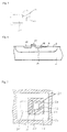
- FIG. 1 shows in cross section a diode realized in CMOS technology, which is p-doped Substrate 1 is embedded.
- the diode consists of a p-well 2, which is completely within an n-well 3 is located.
- the invention is based on the knowledge that the breakdown voltage of formed between the two wells 2 and 3 pn junction through openings along the lateral edge 4 of the pn junction is limited. The reason for this is that the concentration of the Ions of the n-well 3 is greatest at these points and that at point 4 a field increase (so-called peak effect) occurs.
- the n-well 3 it is now proposed to concentrate the ions in the critical region of the p-n to reduce the transition by using a mask during the implantation to form the n-well 3 is used, which covers a part of the later n-well 3, namely the part in which the edge of the p-tub 2 comes to rest. Because the n-well 3 must be contacted ohmic, the Implantation of the n-well 3 initially produces two n-doped regions, but the distance between them is dimensioned in this way is that the two separate areas become one area in the subsequent diffusions unite. In this way, the concentration of the ions of the n-well 3 in the range of significantly reduce the lateral edge of the p-well 2 and thus the breakdown voltage of the pn junction increase.
- the invention also enables the production of MOS transistors with improved properties.
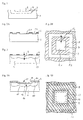
- FIG. 2A shows in cross section a substrate 1 of a first conductivity type, in the surface thereof two separate areas 5.1 and 5.2 of a second conductivity type have been formed by implantation are. During the implantation, a mask 6 covers those areas that are not to be doped. If If a p-doped substrate 1 is used, then the first conductivity type is p-conductive and the second Conductivity type n-type. If an n-doped substrate 1 is used, then the first one Conductivity type n-type and the second conductivity type p-type.
- the mask 6 has two openings, namely a central window 7 and a circumferential strip 8, which are separated by a covering strip 9, so that the two separate regions 5.1 and 5.2 of the second conductivity type initially arise during the implantation.
- the width d 1 of the covering strip 9 is dimensioned such that the two separate regions 5.1 and 5.2 of the second conductivity type unite in the subsequent diffusion process or processes as a result of the lateral diffusion to form a single trough 10 of the second conductivity type. This state is shown in FIG. 3.
- the width d 1 of the covering strip 9 of the mask 6 is approximately as large as the depth t of the trough 10.
- FIG. 4A shows the mask 11, which is used during the implantation of an area 12 of the first conductivity type, which is completely within the tub 10 is used. Is drawn with a dashed line also the position of the mask 6, which was used for the production of the tub 10.
- the mask 11 faces a window 13, the edge 14 of which is approximately in the middle of the covering strip 9 of the mask 6 lies.
- the mask 11 thus completely covers the area 5.1 defined by the mask 6.
- the area 12 area 5.1 completely defined by mask 6 overlaps and is larger than area 5.1.
- the Area 12 does not affect area 5.2.
- FIG. 4B shows the mask 11 in a top view.
- the position of the mask 6, which was used for the production of the tub 10, is again shown with a dashed line.
- a diffusion process takes place, which primarily serves to electrically activate the implanted ions.
- the area 12 now forms a trough 15 of the first conductivity type.
- the two tubs 10 and 15 form a pn junction.
- the concentration of the ions in the tub 10 is now lower than in the case of a conventional pn junction. so that a higher breakdown voltage results.
- a pn transition results, in which the Breakthrough is now no longer along the lateral edge 4. but in the central, flat area 16 of the pn junction.
- a pn junction produced in this way is suitable for operation as a diode with increased breakdown voltage or for operation as an avalanche photodiode with improved light sensitivity.
- the second area 5.2 also serves for the ohmic contacting of the tub 10, for which purpose at least a part of the second area 5.2 is heavily endowed with a further implantation process. It now depends on the tolerances that can be achieved when aligning masks 6 and 11. whether the second area 5.2 as circumferential strip 8 is to be formed.
- the window 13 in the mask 11 is then in any case larger than the area 5.1, but smaller than the diffused tub 10.
- a highly doped offers circumferential strip 8 but the advantage of minimal internal resistance.
- FIG. 5 shows the layout of the mask 6 for the production of the trough 10 of the second conductivity type and the mask 11 of the well 15 of the first conductivity type for an arrangement where the second Area 5.2 is only so large that the electrical contacting of the tub 10 can be done properly.
- FIG. 6 shows a p-channel MOS transistor in cross section, which is inserted into a p-doped substrate 1 diffused n-well 3.
- two p ++ doped regions serving as source 17 and drain 18 and a gate 19 has.
- a mask 20 is used in the n-well implantation, in which a Part of the rectangular window which was conventional in the prior art was covered.
- the mask 20 for the n-well 3 does not contain a single window 21, as shown in FIG. 7, but two windows 21 and 22, which are separated by a strip-shaped area 23.
- the two n-doped regions 5.1 and 5.2 remain but now not separately, but due to the sideways diffusion, they unite two n-doped regions 5.1 and 5.2 to the n-well 3 (Fig. 6).
- the mask for the implantation of the drain 18 has one shown with a dash-dotted border Window 24, which is larger than the window 22, so that its edge within the strip-shaped Area 23 is where the concentration of the ions of the n-well 3 compared to those from the prior art Technology known MOS transistors is reduced.
- the window 24 ' is also of the source.
- the breakdown voltage between drain 18 and n-well 3 is therefore analog to the example of the diode explained above no longer through openings in the area of the side Edge 4 (FIG. 6) of the drain 18 is limited, but by openings in the central, flat area 16.
- the threshold voltage of the MOS transistor can also be reduced when the gate 19 is complete is arranged above the strip-shaped region 23, since there the doping of the n-well 3 is reduced.
- the pn junctions described can be used, for example, in the known CMOS technology deploy. In this way, highly sensitive photosensors can be used with the associated Signal processing circuit can be realized on a single semiconductor chip. Such photosensors can also be equipped with an optical anti-reflection filter that is adapted to the spectral range of the flame used in flame monitoring or as CMOS compatible photosensors two-dimensional image sensor can be expanded. For dimensioning examples for the doping for UV photosensors are expressly referred to the patent EP 296 371 cited at the beginning.
Landscapes
- Light Receiving Elements (AREA)
- Insulated Gate Type Field-Effect Transistor (AREA)
- Solid State Image Pick-Up Elements (AREA)
- Metal-Oxide And Bipolar Metal-Oxide Semiconductor Integrated Circuits (AREA)
Abstract
Description
- Fig. 1
- den pn-Übergang einer konventionellen Diode.
- Fig. 2 - 4
- verschiedene Schritte bei der Herstellung einer erfindungsgemässen Diode,
- Fig. 5
- das Layout der Masken für die Herstellung einer weiteren erfindungsgemässen Diode, und
- Fig. 6, 7
- einen p-Kanal MOS Transistor.
Claims (4)
- Verfahren zur Herstellung eines pn-Überganges in einem Halbleiterbauteil, dadurch gekennzeichnet, dassinnerhalb eines Gebietes (1) eines ersten Leitfähigkeitstyps durch Implantation ein erstes und ein zweites Gebiet (5.1, 5.2) eines zweiten Leitfähigkeitstyps gebildet werden, die zunächst voneinander getrennt sind,sich das erste und das zweite Gebiet (5.1, 5.2) bei nachfolgenden Diffusionsprozessen infolge seitlicher Diffusion zu einer zusammenhängenden Wanne (10) vereinigen,durch Implantation ein weiteres Gebiet (12) des ersten Leitfähigkeitstyps gebildet wird, das das erste Gebiet (5.1) des zweiten Leitfähigkeitstyps vollständig überlappt und das grösser ist als das erste Gebiet (5.1), und das das zweite Gebiet (5.2) des zweiten Leitfähigkeitstyps nicht berührt.
- Flammendetektor für einen Brenner, mit einem Photosensor mit einem nach dem Verfahren nach Anspruch 1 hergestellten pn-Übergang.
- MOS Transistor mit einer Wanne (3), die n- oder p-leitend ist, wobei der pn-Übergang zwischen Drain (18) und der Wanne (3) nach dem Verfahren nach Anspruch 1 hergestellt wurde.
- Bildsensor mit Photosensoren, die je einen nach dem Verfahren nach Anspruch 1 hergestellten pn-Übergang aufweisen.
Priority Applications (4)
| Application Number | Priority Date | Filing Date | Title |
|---|---|---|---|
| DE50014864T DE50014864D1 (de) | 2000-09-20 | 2000-09-20 | Verfahren zur Herstellung eines Halbleiter-Photosensors |
| EP00810853A EP1191598B1 (de) | 2000-01-18 | 2000-09-20 | Verfahren zur Herstellung eines Halbleiter-Photosensors |
| US09/690,218 US6376321B1 (en) | 2000-01-18 | 2000-10-17 | Method of making a pn-junction in a semiconductor element |
| JP2001283511A JP2002190615A (ja) | 2000-01-18 | 2001-09-18 | 半導体モジュールにおけるpn接合の製造方法、炎検知器、MOSトランジスタおよびイメージセンサ |
Applications Claiming Priority (4)
| Application Number | Priority Date | Filing Date | Title |
|---|---|---|---|
| US49431600A | 2000-01-18 | 2000-01-18 | |
| US23407700P | 2000-09-20 | 2000-09-20 | |
| EP00810853A EP1191598B1 (de) | 2000-01-18 | 2000-09-20 | Verfahren zur Herstellung eines Halbleiter-Photosensors |
| US09/690,218 US6376321B1 (en) | 2000-01-18 | 2000-10-17 | Method of making a pn-junction in a semiconductor element |
Publications (2)
| Publication Number | Publication Date |
|---|---|
| EP1191598A1 true EP1191598A1 (de) | 2002-03-27 |
| EP1191598B1 EP1191598B1 (de) | 2007-12-19 |
Family
ID=32034284
Family Applications (1)
| Application Number | Title | Priority Date | Filing Date |
|---|---|---|---|
| EP00810853A Expired - Lifetime EP1191598B1 (de) | 2000-01-18 | 2000-09-20 | Verfahren zur Herstellung eines Halbleiter-Photosensors |
Country Status (3)
| Country | Link |
|---|---|
| US (1) | US6376321B1 (de) |
| EP (1) | EP1191598B1 (de) |
| JP (1) | JP2002190615A (de) |
Cited By (4)
| Publication number | Priority date | Publication date | Assignee | Title |
|---|---|---|---|---|
| US7262402B2 (en) | 2005-02-14 | 2007-08-28 | Ecole Polytechnique Federal De Lausanne | Integrated imager circuit comprising a monolithic array of single photon avalanche diodes |
| US7501628B2 (en) | 2005-02-14 | 2009-03-10 | Ecole Polytechnique Federale De Lausanne Epfl | Transducer for reading information stored on an optical record carrier, single photon detector based storage system and method for reading data from an optical record carrier |
| US7547872B2 (en) | 2005-02-14 | 2009-06-16 | Ecole Polytechnique Federale De Lausanne | Integrated circuit comprising an array of single photon avalanche diodes |
| US7683308B2 (en) | 2004-01-12 | 2010-03-23 | Ecole Polytechnique Federale de Lausanne EFPL | Controlling spectral response of photodetector for an image sensor |
Families Citing this family (7)
| Publication number | Priority date | Publication date | Assignee | Title |
|---|---|---|---|---|
| US6500723B1 (en) * | 2001-10-05 | 2002-12-31 | Motorola, Inc. | Method for forming a well under isolation and structure thereof |
| DE10302632B4 (de) * | 2003-01-23 | 2004-11-11 | Austriamicrosystems Ag | Verfahren zum Erzeugen eines definierten Dotierungsgebietes in einem Halbleitermaterial |
| JP2006173487A (ja) * | 2004-12-17 | 2006-06-29 | Omron Corp | 撮像デバイス |
| EP1679749A1 (de) * | 2005-01-11 | 2006-07-12 | Ecole Polytechnique Federale De Lausanne Epfl - Sti - Imm - Lmis3 | Halbleiter Photodiode und Verfahren zur Herstellung |
| EP1936390A1 (de) * | 2006-12-20 | 2008-06-25 | Ecole Polytechnique Federale De Lausanne Epfl - Sti - Imm - Lmis3 | Halbleiterbauteil zum Messen von ultra kleinen elektrischen Strömen und kleinen Spannungen |
| CN111628020B (zh) * | 2020-05-19 | 2021-10-08 | 华中科技大学 | 一种基于TMDCs横向PIN同质结的光电二极管及制备方法 |
| CN112582293B (zh) * | 2020-12-09 | 2021-08-13 | 北京智创芯源科技有限公司 | 一种离子激活的检测方法 |
Citations (8)
| Publication number | Priority date | Publication date | Assignee | Title |
|---|---|---|---|---|
| US3735210A (en) * | 1971-06-07 | 1973-05-22 | Rca Corp | Zener diode for monolithic integrated circuits |
| US4127859A (en) * | 1977-02-25 | 1978-11-28 | National Semiconductor Corporation | Integrated circuit subsurface zener diode |
| JPS57122579A (en) * | 1981-01-22 | 1982-07-30 | Mitsubishi Electric Corp | Zener diode |
| US4683483A (en) * | 1986-05-05 | 1987-07-28 | Burr-Brown Corporation | Subsurface zener diode and method of making |
| EP0296371A1 (de) * | 1987-06-22 | 1988-12-28 | Landis & Gyr Business Support AG | Photodetektor für Ultraviolett und Verfahren zur Herstellung |
| US5298788A (en) * | 1991-06-28 | 1994-03-29 | Sgs-Thomson Microelectronics S.A. | Avalanche diode in a bipolar integrated circuit |
| DE4329837A1 (de) * | 1993-09-03 | 1995-03-09 | Gold Star Electronics | Verfahren zum Herstellen eines Silizium-Halbleiterbauelements |
| EP0948038A1 (de) * | 1998-03-31 | 1999-10-06 | STMicroelectronics SA | Herstellungsverfahren für eine Avalanche-Diode mit steuerbarem Schwellwert |
Family Cites Families (1)
| Publication number | Priority date | Publication date | Assignee | Title |
|---|---|---|---|---|
| US4999309A (en) * | 1990-07-12 | 1991-03-12 | National Semiconductor Corporation | Aluminum-implant leakage reduction |
-
2000
- 2000-09-20 EP EP00810853A patent/EP1191598B1/de not_active Expired - Lifetime
- 2000-10-17 US US09/690,218 patent/US6376321B1/en not_active Expired - Lifetime
-
2001
- 2001-09-18 JP JP2001283511A patent/JP2002190615A/ja active Pending
Patent Citations (8)
| Publication number | Priority date | Publication date | Assignee | Title |
|---|---|---|---|---|
| US3735210A (en) * | 1971-06-07 | 1973-05-22 | Rca Corp | Zener diode for monolithic integrated circuits |
| US4127859A (en) * | 1977-02-25 | 1978-11-28 | National Semiconductor Corporation | Integrated circuit subsurface zener diode |
| JPS57122579A (en) * | 1981-01-22 | 1982-07-30 | Mitsubishi Electric Corp | Zener diode |
| US4683483A (en) * | 1986-05-05 | 1987-07-28 | Burr-Brown Corporation | Subsurface zener diode and method of making |
| EP0296371A1 (de) * | 1987-06-22 | 1988-12-28 | Landis & Gyr Business Support AG | Photodetektor für Ultraviolett und Verfahren zur Herstellung |
| US5298788A (en) * | 1991-06-28 | 1994-03-29 | Sgs-Thomson Microelectronics S.A. | Avalanche diode in a bipolar integrated circuit |
| DE4329837A1 (de) * | 1993-09-03 | 1995-03-09 | Gold Star Electronics | Verfahren zum Herstellen eines Silizium-Halbleiterbauelements |
| EP0948038A1 (de) * | 1998-03-31 | 1999-10-06 | STMicroelectronics SA | Herstellungsverfahren für eine Avalanche-Diode mit steuerbarem Schwellwert |
Non-Patent Citations (1)
| Title |
|---|
| PATENT ABSTRACTS OF JAPAN vol. 006, no. 218 (E - 139) 2 November 1982 (1982-11-02) * |
Cited By (5)
| Publication number | Priority date | Publication date | Assignee | Title |
|---|---|---|---|---|
| US7683308B2 (en) | 2004-01-12 | 2010-03-23 | Ecole Polytechnique Federale de Lausanne EFPL | Controlling spectral response of photodetector for an image sensor |
| US7262402B2 (en) | 2005-02-14 | 2007-08-28 | Ecole Polytechnique Federal De Lausanne | Integrated imager circuit comprising a monolithic array of single photon avalanche diodes |
| US7501628B2 (en) | 2005-02-14 | 2009-03-10 | Ecole Polytechnique Federale De Lausanne Epfl | Transducer for reading information stored on an optical record carrier, single photon detector based storage system and method for reading data from an optical record carrier |
| US7547872B2 (en) | 2005-02-14 | 2009-06-16 | Ecole Polytechnique Federale De Lausanne | Integrated circuit comprising an array of single photon avalanche diodes |
| US8168934B2 (en) | 2005-02-14 | 2012-05-01 | Ecole Polytechnique Federale De Lausanne | Integrated circuit comprising an array of single photon avalanche diodes |
Also Published As
| Publication number | Publication date |
|---|---|
| JP2002190615A (ja) | 2002-07-05 |
| EP1191598B1 (de) | 2007-12-19 |
| US6376321B1 (en) | 2002-04-23 |
Similar Documents
| Publication | Publication Date | Title |
|---|---|---|
| DE69925091T2 (de) | Aktiver Pixelsensor für Farbdetektion | |
| DE69321822T2 (de) | Photodiodenstruktur | |
| DE68917242T2 (de) | Festkörperbildsensor. | |
| DE19630434C2 (de) | Bipolarphototransistorpixelelement | |
| DE19908457B4 (de) | CMOS-Bildsensor und Photodiode und Verfahren zur Herstellung | |
| DE60031221T2 (de) | Photodiode für einen CMOS Bildsensor mit einem schwebenden Dotierungsbereich | |
| DE4116694C2 (de) | Mit einer Fotodiode versehene Halbleitervorrichtung und Verfahren zu ihrer Herstellung | |
| DE2802987A1 (de) | Festkoerper-abbildungsvorrichtung | |
| DE2940343A1 (de) | Photodiodenvorrichtung | |
| DE10105071A1 (de) | CMOS-Bildsensor und Verfahren zu dessen Herstellung | |
| EP1357393A1 (de) | Vorrichtung zur Ermittlung des Einfallwinkels einer Strahlung auf eine Strahlungseinfallfläche | |
| DE69331357T2 (de) | Photoelektrische Umwandlungsvorrichtung | |
| EP1191598B1 (de) | Verfahren zur Herstellung eines Halbleiter-Photosensors | |
| DE4412671C2 (de) | Ausgangstreiber-Feldeffekttransistor eines ladungsgekoppelten Bildsensorbauelementes | |
| DE102008046260A1 (de) | Bildsensor und Verfahren zu dessen Herstellung | |
| DE3706278C2 (de) | ||
| WO2001022494A1 (de) | Vertikale pixelzellen | |
| DE10251735B4 (de) | Aktives Pixel und Verfahren zur Herstellung eines aktiven Pixels | |
| DE2804466A1 (de) | Festkoerper-aufnahmeeinrichtung | |
| DE4310915B4 (de) | Festkörperbildsensor mit hohem Signal-Rauschverhältnis | |
| DE102005026629B4 (de) | Bildsensor und zugehöriges Herstellungsverfahren | |
| DE69025173T2 (de) | Festkörper-bildsensor | |
| US5734191A (en) | Contactless capacitor-coupled bipolar active pixel sensor with integrated electronic shutter | |
| DE3788516T2 (de) | Ausgangskreis für abbildungssensor. | |
| DE112020006344T5 (de) | Range-Imaging-Sensor und Verfahren zur Herstellung dieses Sensors |
Legal Events
| Date | Code | Title | Description |
|---|---|---|---|
| PUAI | Public reference made under article 153(3) epc to a published international application that has entered the european phase |
Free format text: ORIGINAL CODE: 0009012 |
|
| AK | Designated contracting states |
Kind code of ref document: A1 Designated state(s): AT BE CH CY DE DK ES FI FR GB GR IE IT LI LU MC NL PT SE |
|
| AX | Request for extension of the european patent |
Free format text: AL;LT;LV;MK;RO;SI |
|
| 17P | Request for examination filed |
Effective date: 20020926 |
|
| AKX | Designation fees paid |
Free format text: AT BE CH CY DE DK ES FI FR GB GR IE IT LI LU MC NL PT SE |
|
| RBV | Designated contracting states (corrected) |
Designated state(s): CH DE FR LI NL |
|
| RAP1 | Party data changed (applicant data changed or rights of an application transferred) |
Owner name: SIEMENS SCHWEIZ AG |
|
| 17Q | First examination report despatched |
Effective date: 20060908 |
|
| 17Q | First examination report despatched |
Effective date: 20060908 |
|
| GRAP | Despatch of communication of intention to grant a patent |
Free format text: ORIGINAL CODE: EPIDOSNIGR1 |
|
| RTI1 | Title (correction) |
Free format text: METHOD FOR FABRICATING A SEMICONDUCTOR PHOTOSENSOR |
|
| GRAS | Grant fee paid |
Free format text: ORIGINAL CODE: EPIDOSNIGR3 |
|
| GRAA | (expected) grant |
Free format text: ORIGINAL CODE: 0009210 |
|
| AK | Designated contracting states |
Kind code of ref document: B1 Designated state(s): CH DE FR LI NL |
|
| REG | Reference to a national code |
Ref country code: CH Ref legal event code: EP |
|
| REF | Corresponds to: |
Ref document number: 50014864 Country of ref document: DE Date of ref document: 20080131 Kind code of ref document: P |
|
| PG25 | Lapsed in a contracting state [announced via postgrant information from national office to epo] |
Ref country code: NL Free format text: LAPSE BECAUSE OF FAILURE TO SUBMIT A TRANSLATION OF THE DESCRIPTION OR TO PAY THE FEE WITHIN THE PRESCRIBED TIME-LIMIT Effective date: 20071219 |
|
| NLV1 | Nl: lapsed or annulled due to failure to fulfill the requirements of art. 29p and 29m of the patents act | ||
| EN | Fr: translation not filed | ||
| PLBE | No opposition filed within time limit |
Free format text: ORIGINAL CODE: 0009261 |
|
| STAA | Information on the status of an ep patent application or granted ep patent |
Free format text: STATUS: NO OPPOSITION FILED WITHIN TIME LIMIT |
|
| 26N | No opposition filed |
Effective date: 20080922 |
|
| REG | Reference to a national code |
Ref country code: CH Ref legal event code: PCOW Free format text: SIEMENS SCHWEIZ AG;FREILAGERSTRASSE 40;8047 ZUERICH (CH) |
|
| PG25 | Lapsed in a contracting state [announced via postgrant information from national office to epo] |
Ref country code: FR Free format text: LAPSE BECAUSE OF FAILURE TO SUBMIT A TRANSLATION OF THE DESCRIPTION OR TO PAY THE FEE WITHIN THE PRESCRIBED TIME-LIMIT Effective date: 20081010 |
|
| PGFP | Annual fee paid to national office [announced via postgrant information from national office to epo] |
Ref country code: DE Payment date: 20141120 Year of fee payment: 15 Ref country code: CH Payment date: 20141204 Year of fee payment: 15 |
|
| REG | Reference to a national code |
Ref country code: DE Ref legal event code: R119 Ref document number: 50014864 Country of ref document: DE |
|
| REG | Reference to a national code |
Ref country code: CH Ref legal event code: PL |
|
| PG25 | Lapsed in a contracting state [announced via postgrant information from national office to epo] |
Ref country code: DE Free format text: LAPSE BECAUSE OF NON-PAYMENT OF DUE FEES Effective date: 20160401 Ref country code: CH Free format text: LAPSE BECAUSE OF NON-PAYMENT OF DUE FEES Effective date: 20150930 Ref country code: LI Free format text: LAPSE BECAUSE OF NON-PAYMENT OF DUE FEES Effective date: 20150930 |