EP1179858A2 - Light emitting devices - Google Patents
Light emitting devices Download PDFInfo
- Publication number
- EP1179858A2 EP1179858A2 EP01306793A EP01306793A EP1179858A2 EP 1179858 A2 EP1179858 A2 EP 1179858A2 EP 01306793 A EP01306793 A EP 01306793A EP 01306793 A EP01306793 A EP 01306793A EP 1179858 A2 EP1179858 A2 EP 1179858A2
- Authority
- EP
- European Patent Office
- Prior art keywords
- light emitter
- base substrate
- light
- projecting platform
- platform
- Prior art date
- Legal status (The legal status is an assumption and is not a legal conclusion. Google has not performed a legal analysis and makes no representation as to the accuracy of the status listed.)
- Granted
Links
Images

Classifications
-
- H—ELECTRICITY
- H10—SEMICONDUCTOR DEVICES; ELECTRIC SOLID-STATE DEVICES NOT OTHERWISE PROVIDED FOR
- H10H—INORGANIC LIGHT-EMITTING SEMICONDUCTOR DEVICES HAVING POTENTIAL BARRIERS
- H10H20/00—Individual inorganic light-emitting semiconductor devices having potential barriers, e.g. light-emitting diodes [LED]
- H10H20/80—Constructional details
- H10H20/85—Packages
- H10H20/8506—Containers
-
- H—ELECTRICITY
- H10—SEMICONDUCTOR DEVICES; ELECTRIC SOLID-STATE DEVICES NOT OTHERWISE PROVIDED FOR
- H10H—INORGANIC LIGHT-EMITTING SEMICONDUCTOR DEVICES HAVING POTENTIAL BARRIERS
- H10H20/00—Individual inorganic light-emitting semiconductor devices having potential barriers, e.g. light-emitting diodes [LED]
- H10H20/80—Constructional details
- H10H20/85—Packages
- H10H20/851—Wavelength conversion means
- H10H20/8514—Wavelength conversion means characterised by their shape, e.g. plate or foil
-
- H—ELECTRICITY
- H10—SEMICONDUCTOR DEVICES; ELECTRIC SOLID-STATE DEVICES NOT OTHERWISE PROVIDED FOR
- H10H—INORGANIC LIGHT-EMITTING SEMICONDUCTOR DEVICES HAVING POTENTIAL BARRIERS
- H10H20/00—Individual inorganic light-emitting semiconductor devices having potential barriers, e.g. light-emitting diodes [LED]
- H10H20/01—Manufacture or treatment
- H10H20/036—Manufacture or treatment of packages
- H10H20/0361—Manufacture or treatment of packages of wavelength conversion means
-
- H—ELECTRICITY
- H10—SEMICONDUCTOR DEVICES; ELECTRIC SOLID-STATE DEVICES NOT OTHERWISE PROVIDED FOR
- H10W—GENERIC PACKAGES, INTERCONNECTIONS, CONNECTORS OR OTHER CONSTRUCTIONAL DETAILS OF DEVICES COVERED BY CLASS H10
- H10W72/00—Interconnections or connectors in packages
- H10W72/01—Manufacture or treatment
- H10W72/015—Manufacture or treatment of bond wires
- H10W72/01515—Forming coatings
-
- H—ELECTRICITY
- H10—SEMICONDUCTOR DEVICES; ELECTRIC SOLID-STATE DEVICES NOT OTHERWISE PROVIDED FOR
- H10W—GENERIC PACKAGES, INTERCONNECTIONS, CONNECTORS OR OTHER CONSTRUCTIONAL DETAILS OF DEVICES COVERED BY CLASS H10
- H10W72/00—Interconnections or connectors in packages
- H10W72/071—Connecting or disconnecting
- H10W72/075—Connecting or disconnecting of bond wires
-
- H—ELECTRICITY
- H10—SEMICONDUCTOR DEVICES; ELECTRIC SOLID-STATE DEVICES NOT OTHERWISE PROVIDED FOR
- H10W—GENERIC PACKAGES, INTERCONNECTIONS, CONNECTORS OR OTHER CONSTRUCTIONAL DETAILS OF DEVICES COVERED BY CLASS H10
- H10W72/00—Interconnections or connectors in packages
- H10W72/50—Bond wires
- H10W72/531—Shapes of wire connectors
- H10W72/536—Shapes of wire connectors the connected ends being ball-shaped
-
- H—ELECTRICITY
- H10—SEMICONDUCTOR DEVICES; ELECTRIC SOLID-STATE DEVICES NOT OTHERWISE PROVIDED FOR
- H10W—GENERIC PACKAGES, INTERCONNECTIONS, CONNECTORS OR OTHER CONSTRUCTIONAL DETAILS OF DEVICES COVERED BY CLASS H10
- H10W72/00—Interconnections or connectors in packages
- H10W72/50—Bond wires
- H10W72/531—Shapes of wire connectors
- H10W72/5363—Shapes of wire connectors the connected ends being wedge-shaped
-
- H—ELECTRICITY
- H10—SEMICONDUCTOR DEVICES; ELECTRIC SOLID-STATE DEVICES NOT OTHERWISE PROVIDED FOR
- H10W—GENERIC PACKAGES, INTERCONNECTIONS, CONNECTORS OR OTHER CONSTRUCTIONAL DETAILS OF DEVICES COVERED BY CLASS H10
- H10W90/00—Package configurations
- H10W90/701—Package configurations characterised by the relative positions of pads or connectors relative to package parts
- H10W90/751—Package configurations characterised by the relative positions of pads or connectors relative to package parts of bond wires
- H10W90/756—Package configurations characterised by the relative positions of pads or connectors relative to package parts of bond wires between a chip and a stacked lead frame, conducting package substrate or heat sink
Definitions
- the present invention concerns light emitting devices, such as light emitting diode devices, and methods of construction of such devices.
- LEDs Light emitting diodes
- solid state illuminating devices commonly used for illuminators, display components and indication devices.
- Early LEDs provided radiation in the high frequency end of the visible spectrum, namely as red light. More recently, LEDs have been developed that operate efficiently in the higher frequency portion of the visible spectrum, namely to emit blue light.
- Such devices employ layers of luminescent or fluorescent materials, for example phosphor, overlying the LED die and serving to shift the wavelength of the light emitted from the die, the radiation being re-emitted from the intermediate phosphor layer at a longer wavelength.
- a blue LED such as a gallium nitride (GaN) die
- GaN gallium nitride
- a blue LED such as a gallium nitride (GaN) die
- GaN gallium nitride
- the phosphor layer serves to absorb, shift, and re-emit a broad band yellow-green light, as well as some unabsorbed original blue light which passes through the phosphor layer.
- the combination radiation is emitted through the epoxy lens and results to a viewer in a perceived emission of white light.
- the dye used for "doping" the epoxy material in constructing this type of LED device can be provided by way of an inorganic dye material, generally a powder, or by way of an organic dye material, generally a liquid.
- an inorganic dye material generally a powder
- organic dye material generally a liquid.
- a yellow ring can be seen around the perimeter of the radiation pattern. Therefore, viewing the lamp on-axis and off-axis can result in perception of different colours.
- the reason for this artefact has been found to be that the quantity of luminescent or fluorescent material surrounding the LED die tends to be non-uniform, due to the method of construction of such devices.
- the doped epoxy material is conventionally applied over the LED die in a quantity such that it fills the reflector cup in which the die is mounted. The phosphor particles contained in the epoxy material then settle around the contours of the LED die and reflector cup as the epoxy cures.
- the present invention seeks to provide improved light emitting devices.
- the invention provides, in a first aspect, a light emitting device comprising a light emitter disposed above a base substrate and a coating material applicable over the light emitter, the base substrate having a projecting platform on which the light emitter is mounted, such that the projecting platform supports the light emitter at a prescribed distance from the surrounding base substrate.
- the projecting platform may be formed as an integral part of the base substrate, or may be provided as a discrete component, attachable to said base substrate, in which case the projecting platform and the base substrate may be fabricated from different materials.
- the base substrate comprises a planar base portion and a sloping wall portion to provide reflection of light emitted by said light emitter.
- the sloping wall is preferably of frusto-conical form surrounding the projecting platform, so as to provide a generally annular planar base portion around said projecting platform.
- the base substrate is coated with a reflective medium, such as silver, and this reflective coating may also cover the surface of the projecting platform.
- a reflective medium such as silver
- the preferred embodiment provides, then, a lowered portion of the base substrate relative to the base of the light emitter, into which lowered portion excess applied dye material is able to flow.
- This allows the layer of dye material which remains over the sides of the light emitter to assume a lower thickness than would otherwise be possible, and ideally to take an approximately uniform thickness over the LED die, so reducing the variation in energy transmission across the light emitting device.
- the device has particular application to doped LED construction using inorganic phosphor dye material.
- the invention provides a method of providing a light emitting device, the method comprising the steps of providing a base substrate having a projecting platform; providing a light emitter having a top surface and side surfaces; positioning the light emitter on said projecting platform such that the light emitter is supported at a prescribed distance from the surrounding base substrate; applying over the light emitter a settable coating material containing a dye compound in such a manner that, when the coating material has set, the dye compound covering the light emitter is of a comparable thickness over the side surfaces as over the top surface of the light emitter, excess dye compound being deposited over said surrounding base substrate.
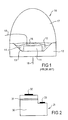
- the LED device of the prior art shows a device 10 used to produce white light from a blue emitting die 11.
- Blue die 11 is provided by a substantially rectangular tab of gallium nitride (GaN) substrate bonded to the surface of a reflector cup support 12, typically of lead, or a PCB frame.
- reflector cup 12 provides a substantially planar base surface 13 and sloping wall 14, which, for light reflecting purposes, has an overall frusto-conical shaping.
- the LED die 11 is arranged approximately centrally on the planar base surface of the reflector cup as shown in the figure, and the device operates to provide a very high intensity of upward-directed light.
- Contact wires 18 are applied to the device as shown, in order to apply electrical power to die 11.
- Cerium activated Yttrium Aluminium Garnet (YAG:Ce 3 +) phosphor 15 in an epoxy matrix 16 is poured over LED die 11, and the entire construction then over-moulded with a conventional clear epoxy lens 17.
- the YAG:Ce 3 + phosphor re-emits broad band yellow-green light and some unabsorbed original blue light which is transmitted through phosphor layer 15, to give a perceived combination radiation of white light.
- luminescent/fluorescent layers in combination with a blue die light source permits light emission at various different wavelengths.
- possible fluorescent materials include the following phosphors available from SRAM Sylvan Inc. (Danvers, Massachusetts): Ag:ZnS (blue); CuAuAl:ZnS (green); CuAl:ZnS (green); Mg4(F)Ge05:Mn (red); Ce:YAG (yellow-green).
- the phosphor material Since the specific gravity of the phosphor particles is significantly higher than the epoxy material in which they are carried, the phosphor material begins to settle within the epoxy matrix to follow the contours of the substrate. A large proportion of the phosphor material 15 settles in the annular region between the sides of the LED die 11 and the conical wall 14 of the reflector cup 12, only a relatively thin layer remaining overlying LED die 11, as Figure 1 illustrates. When the phosphor material has settled and the epoxy cured, the result is a two-layer coating, of clear epoxy layer 16 overlying phosphor dye layer 15.
- a first embodiment of device is illustrated in Figure 3 by use of similar reference numerals to those used with respect to the prior art device of Figure 1, each reference numeral increased by 10 for corresponding components.
- the LED device 20 features a modified construction of reflector cup 22, having a planar projecting portion defining a raised platform 29 approximately centrally within base 23 of reflector cup 22.
- the raised platform forms the supporting base for LED die 21.
- LED die 21 is mounted on and bonded to raised platform 29, and electrical connection wires 28 attached to the die to provide electrical power.
- a luminescent material is then applied over LED die 21, in the known form of an epoxy material 26 containing inorganic phosphor powder which has been premixed with epoxy 26 to form a viscous slurry. The applied material flows over die 21 and platform 29 to fill reflector cup 22. Due to the outer annular trough provided by reflector cup base 23, inclined wall 24, and the sides of raised platform 29, the particulate phosphor material 25 is able to settle to a lower position towards the periphery of reflector cup 22 than would otherwise be the case, as Figure 3 shows.
- the thickness of the dye material around the sides of LED die 21 is therefore significantly reduced in comparison with that provided in an equivalent prior art device.
- the thickness of the luminescent material may be approximately constant over the entire surface and sides of die 21.
- a rectangular raised platform 29 was used, supporting a similarly shaped LED die 21.
- the LED die used was approximately 0.1 mm in thickness, supported on a platform 29 slightly larger than die 21 (by about 0.1 mm on all sides) to ensure sufficient phosphor material 25 is able remains around die 21.
- Clearly platform 29 can be shaped and sized as appropriate to match the shape and dimensions of die 21.
- Reflector cup 22 is made from copper or steel or other metal, on which a reflective silver layer is typically applied.
- the silver layer also coats platform 29, since light does travel downwardly from LED die 21, and should be reflected back in an upward direction to increase the efficiency of device 20.
- the entire reflector cup, including platform 29, is stamped into the substrate material by means of a stamping tool, and LED die 21, as well as the electrical lead wires 28, are then introduced to the device.
- FIG 4 Another embodiment, shown in Figure 4, provides the same geometry of the device of Figure 3, but involves the use of a raised platform 29a provided by a separate rectangular platform component as shown.
- Platform 29a is bonded to base 23 of the reflector cup 22.
- the advantage of this embodiment is that a separate material can be used to provide platform 29a if different characteristics of the reflector cup components are desirable.
- a diamond platform 29a may be used with a high power LED device for purposes of improved heat dissipation away from the LED die 21. Molybdenum, a less expensive alternative to diamond, may also be used for this purpose.
- the epoxy lens overlying the components of the LED device is not shown, but that any suitable such lens may be used with the device, the shape being selected to meet the desired optical radiation pattern.
- UV-stable epoxy plastic materials as conventionally used, are appropriate for this purpose.
- the epoxy lens may incorporate additional coloured or fluorescent material to modify light transmission from the device. Such "doping" of LED lenses is described further in US patent 5,847,507, the entire contents of which are incorporated herein by reference.
- a conventional LED die is illustrated in Figure 2, as an example of the type of LED suitable for use in the device and arranged to be energised to emit light at a prescribed wavelength by applying an appropriate voltage between electrical terminal leads.
- the LED die has a p-n junction 31 defined between layers of semi-conductor crystal 30, in this case gallium nitride (GaN).
- active junction 31 comprises p-type top layers and n-type bottom layers.
- the positive electrical terminal 32 is provided by an upper conducting pad, whilst the negative electrical terminal is provided by a second conducting pad 33 contacting the lower semiconductor crystal layer.
Landscapes
- Led Device Packages (AREA)
Abstract
Description
Claims (13)
- A light emitting device including a light emitter disposed above a base substrate and a coating material applicable over the light emitter, the base substrate including a projecting platform on which the light emitter is mounted, such that the projecting platform supports the light emitter at a prescribed distance from the surrounding base substrate.
- A device according to claim 1, wherein said projecting platform is either formed as an integral part of the base substrate or is a discrete component attachable to said base substrate.
- A device according to claim 1, wherein said projecting platform is a discrete component attachable to said base substrate and said projecting platform and said base substrate are fabricated from different materials.
- A device according to claim 3, wherein said base substrate comprises a metal and said projecting platform comprises a material able to efficiently dissipate heat generated by said light emitter.
- A device according to any preceding claim, wherein said base substrate includes a planar base portion and a sloping wall portion to provide reflection of light emitted by said light emitter.
- A device according to claim 5, wherein the sloping wall is of frusto-conical form surrounding the projecting platform so as to provide a generally annular planar base portion around said projecting platform.
- A device according to any preceding claim, wherein the base substrate is coated with a reflective medium, such as silver.
- A device according to claim 7, wherein the reflective coating covers the surface of said projecting platform.
- A device according to any preceding claim, wherein the coating material contains a fluorescent or luminescent substance to absorb light of one wavelength and re-emit light of a different wavelength.
- A device according to claim 10, wherein the fluorescent or luminescent substance comprises an inorganic dye.
- A device according to any preceding claim, including a lens to focus emitted light, the lens being positioned over the light emitter and the coating material.
- A device according to any preceding claim, wherein the light emitter is selected from the group of an LED and a laser diode.
- A method of providing a light emitting device, including the steps of:providing a base substrate with a projecting platform;providing a light emitter with a top surface and side surfaces;positioning the light emitter on said projecting platform such that the light emitter is supported at a prescribed distance from the surrounding base substrate;applying over the light emitter a settable coating material containing a dye compound in such a manner that, when the coating material has set, the dye compound covering the light emitter is of a comparable thickness over the side surfaces as over the top surface of the light emitter, excess dye compound being deposited over said surrounding base substrate.
Applications Claiming Priority (2)
| Application Number | Priority Date | Filing Date | Title |
|---|---|---|---|
| MY0003619 | 2000-08-09 | ||
| MYPI20003619 | 2000-08-09 |
Publications (3)
| Publication Number | Publication Date |
|---|---|
| EP1179858A2 true EP1179858A2 (en) | 2002-02-13 |
| EP1179858A3 EP1179858A3 (en) | 2003-07-30 |
| EP1179858B1 EP1179858B1 (en) | 2009-03-18 |
Family
ID=19749469
Family Applications (1)
| Application Number | Title | Priority Date | Filing Date |
|---|---|---|---|
| EP01306793A Expired - Lifetime EP1179858B1 (en) | 2000-08-09 | 2001-08-08 | Light emitting devices |
Country Status (3)
| Country | Link |
|---|---|
| US (1) | US7129638B2 (en) |
| EP (1) | EP1179858B1 (en) |
| DE (1) | DE60137995D1 (en) |
Cited By (13)
| Publication number | Priority date | Publication date | Assignee | Title |
|---|---|---|---|---|
| EP1537603A4 (en) * | 2002-09-04 | 2006-09-20 | Cree Inc | SURFACE MOUNTING POWER PHOTOEMETTER PACKAGE ASSEMBLY |
| DE102005030324A1 (en) * | 2005-06-29 | 2007-02-08 | Lighthouse Technology Co., Ltd | Light-emitting diode package structure for liquid crystal display back light source, has photoluminescent material distributed in encapsulant, where material is excited by light emitted from diode chip and scatters light from chip |
| EP1848042A1 (en) * | 2006-04-21 | 2007-10-24 | LEXEDIS Lighting GmbH | LED package with submount |
| US7309151B2 (en) | 2005-04-11 | 2007-12-18 | Avago Technologies Ecbu Ip (Singapore) Pte. Ltd. | Light emitting panel |
| EP1590420A4 (en) * | 2003-01-29 | 2008-04-30 | Korea Res Inst Chem Tech | PHOSPHORUS BASED ON STRONTIUM SILICATE AND PROC D ASSOCI |
| US7479733B2 (en) | 2005-03-24 | 2009-01-20 | Lighthouse Technology Co., Ltd. | Light-emitting diode package structure, cold cathode flourescent lamp and photoluminescent material thereof |
| US7659551B2 (en) | 2003-05-27 | 2010-02-09 | Cree, Inc. | Power surface mount light emitting die package |
| EP1887637A3 (en) * | 2006-08-08 | 2010-09-15 | LG Electronics Inc. | Light emitting device package and method for manufacturing the same |
| US7980743B2 (en) | 2005-06-14 | 2011-07-19 | Cree, Inc. | LED backlighting for displays |
| EP2315280A3 (en) * | 2009-10-26 | 2012-05-02 | LG Innotek Co., Ltd. | Light emitting device package and lighting system |
| JP2014036083A (en) * | 2012-08-08 | 2014-02-24 | Toshiba Corp | Semiconductor light-emitting device |
| EP2704219A4 (en) * | 2011-04-26 | 2014-11-12 | Nichia Corp | METHOD FOR PRODUCING LIGHT EMITTING DEVICE, AND LIGHT EMITTING DEVICE |
| JP2017022360A (en) * | 2015-07-13 | 2017-01-26 | 豊田合成株式会社 | Method for manufacturing light-emitting device |
Families Citing this family (44)
| Publication number | Priority date | Publication date | Assignee | Title |
|---|---|---|---|---|
| US7928455B2 (en) * | 2002-07-15 | 2011-04-19 | Epistar Corporation | Semiconductor light-emitting device and method for forming the same |
| US7244965B2 (en) | 2002-09-04 | 2007-07-17 | Cree Inc, | Power surface mount light emitting die package |
| JP3910517B2 (en) * | 2002-10-07 | 2007-04-25 | シャープ株式会社 | LED device |
| US7423296B2 (en) * | 2003-02-26 | 2008-09-09 | Avago Technologies Ecbu Ip Pte Ltd | Apparatus for producing a spectrally-shifted light output from a light emitting device utilizing thin-film luminescent layers |
| JP3948417B2 (en) * | 2003-02-28 | 2007-07-25 | ノーリツ鋼機株式会社 | Light source unit |
| US7397177B2 (en) * | 2003-09-25 | 2008-07-08 | Matsushita Electric Industrial Co., Ltd. | LED lamp and method for manufacturing the same |
| US7517728B2 (en) * | 2004-03-31 | 2009-04-14 | Cree, Inc. | Semiconductor light emitting devices including a luminescent conversion element |
| US20080284329A1 (en) * | 2004-06-18 | 2008-11-20 | Koninklijke Philips Electronics, N.V. | Led with Improve Light Emittance Profile |
| EP1862035B1 (en) * | 2005-03-14 | 2013-05-15 | Koninklijke Philips Electronics N.V. | Phosphor in polycrystalline ceramic structure and a light-emitting element comprising same |
| US8669572B2 (en) * | 2005-06-10 | 2014-03-11 | Cree, Inc. | Power lamp package |
| KR20060132298A (en) * | 2005-06-17 | 2006-12-21 | 삼성전기주식회사 | Light emitting device package |
| KR100592508B1 (en) * | 2005-07-15 | 2006-06-26 | 한국광기술원 | High Power LED Package with Beacon Shaped Substrate |
| KR101200400B1 (en) * | 2005-12-01 | 2012-11-16 | 삼성전자주식회사 | White light emitting diode |
| KR101019765B1 (en) * | 2006-01-04 | 2011-03-04 | 로무 가부시키가이샤 | Thin light emitting diode lamp and its manufacturing method |
| US8044412B2 (en) | 2006-01-20 | 2011-10-25 | Taiwan Semiconductor Manufacturing Company, Ltd | Package for a light emitting element |
| US8748915B2 (en) | 2006-04-24 | 2014-06-10 | Cree Hong Kong Limited | Emitter package with angled or vertical LED |
| US7635915B2 (en) | 2006-04-26 | 2009-12-22 | Cree Hong Kong Limited | Apparatus and method for use in mounting electronic elements |
| US20070269915A1 (en) * | 2006-05-16 | 2007-11-22 | Ak Wing Leong | LED devices incorporating moisture-resistant seals and having ceramic substrates |
| JP4211804B2 (en) * | 2006-05-19 | 2009-01-21 | セイコーエプソン株式会社 | Device, film forming method and device manufacturing method |
| US8735920B2 (en) | 2006-07-31 | 2014-05-27 | Cree, Inc. | Light emitting diode package with optical element |
| US8367945B2 (en) | 2006-08-16 | 2013-02-05 | Cree Huizhou Opto Limited | Apparatus, system and method for use in mounting electronic elements |
| US8053799B2 (en) * | 2006-09-29 | 2011-11-08 | Seoul Semiconductor Co., Ltd. | LED package |
| WO2008072185A1 (en) * | 2006-12-15 | 2008-06-19 | Koninklijke Philips Electronics N.V. | Lighting system with dichromatic surfaces |
| US9711703B2 (en) | 2007-02-12 | 2017-07-18 | Cree Huizhou Opto Limited | Apparatus, system and method for use in mounting electronic elements |
| US7851990B2 (en) * | 2007-09-06 | 2010-12-14 | He Shan Lide Electronic Enterprise Company Ltd. | Method for generating low color temperature light and light emitting device adopting the same |
| US10256385B2 (en) | 2007-10-31 | 2019-04-09 | Cree, Inc. | Light emitting die (LED) packages and related methods |
| TWI401820B (en) * | 2007-11-07 | 2013-07-11 | 財團法人工業技術研究院 | Light-emitting element and manufacturing method thereof |
| US8946987B2 (en) | 2007-11-07 | 2015-02-03 | Industrial Technology Research Institute | Light emitting device and fabricating method thereof |
| USD633631S1 (en) | 2007-12-14 | 2011-03-01 | Cree Hong Kong Limited | Light source of light emitting diode |
| USD634863S1 (en) | 2008-01-10 | 2011-03-22 | Cree Hong Kong Limited | Light source of light emitting diode |
| US8049230B2 (en) * | 2008-05-16 | 2011-11-01 | Cree Huizhou Opto Limited | Apparatus and system for miniature surface mount devices |
| JP5458910B2 (en) * | 2009-02-24 | 2014-04-02 | 日亜化学工業株式会社 | Light emitting device |
| CN101499446B (en) * | 2009-02-26 | 2013-10-16 | 光宝电子(广州)有限公司 | Wire frame tablet, packaging structure and LED packaging structure |
| JP5455720B2 (en) * | 2010-03-12 | 2014-03-26 | パナソニック株式会社 | Optical semiconductor package and optical semiconductor device |
| US8450770B2 (en) * | 2010-05-11 | 2013-05-28 | Advanced Semiconductor Engineering, Inc. | Light emitting package structure |
| US8421111B2 (en) | 2010-12-27 | 2013-04-16 | Panasonic Corporation | Light-emitting device and lamp |
| US20130141892A1 (en) * | 2011-01-14 | 2013-06-06 | Panasonic Corporation | Lamp and lighting apparatus |
| US9508904B2 (en) * | 2011-01-31 | 2016-11-29 | Cree, Inc. | Structures and substrates for mounting optical elements and methods and devices for providing the same background |
| US8450175B2 (en) | 2011-02-22 | 2013-05-28 | Micron Technology, Inc. | Methods of forming a vertical transistor and at least a conductive line electrically coupled therewith |
| KR101798884B1 (en) | 2011-05-18 | 2017-11-17 | 삼성전자주식회사 | Light emitting device assembly and head light including the same |
| TW201440255A (en) * | 2013-04-03 | 2014-10-16 | Hung Ta Trading Co Ltd | Method of making white light-emitting elements |
| WO2017047950A1 (en) * | 2015-09-15 | 2017-03-23 | 서울반도체주식회사 | Light-emitting device, and color coordinate measurement apparatus and color coordinate correction method of light-emitting device |
| US20170084502A1 (en) * | 2015-09-15 | 2017-03-23 | Seoul Semiconductor Co., Ltd. | Light emitting device, color coordinate measuring apparatus and color coordinate correction method thereof |
| CN110875409B (en) * | 2018-08-30 | 2025-07-11 | 深圳市聚飞光电股份有限公司 | Highly sealed LED bracket, LED and light-emitting device |
Family Cites Families (19)
| Publication number | Priority date | Publication date | Assignee | Title |
|---|---|---|---|---|
| US3555335A (en) * | 1969-02-27 | 1971-01-12 | Bell Telephone Labor Inc | Electroluminescent displays |
| GB1497115A (en) | 1975-03-20 | 1978-01-05 | Standard Telephones Cables Ltd | Arrangement for indicating the switching state of an optical coupler and optical couplers incorporating such an arrangement |
| JPS55123181A (en) * | 1979-03-15 | 1980-09-22 | Nec Corp | Lead frame for light emitting diode |
| JPH0680841B2 (en) * | 1986-04-07 | 1994-10-12 | 株式会社小糸製作所 | Lighting equipment |
| GB2221570B (en) | 1988-08-04 | 1992-02-12 | Stc Plc | Bonding a semiconductor to a substrate |
| US5019746A (en) * | 1989-12-04 | 1991-05-28 | Hewlett-Packard Company | Prefabricated wire leadframe for optoelectronic devices |
| US5534718A (en) * | 1993-04-12 | 1996-07-09 | Hsi-Huang Lin | LED package structure of LED display |
| DE19638667C2 (en) * | 1996-09-20 | 2001-05-17 | Osram Opto Semiconductors Gmbh | Mixed-color light-emitting semiconductor component with luminescence conversion element |
| US5813753A (en) * | 1997-05-27 | 1998-09-29 | Philips Electronics North America Corporation | UV/blue led-phosphor device with efficient conversion of UV/blues light to visible light |
| US5847507A (en) * | 1997-07-14 | 1998-12-08 | Hewlett-Packard Company | Fluorescent dye added to epoxy of light emitting diode lens |
| JP3617587B2 (en) * | 1997-07-17 | 2005-02-09 | 日亜化学工業株式会社 | Light emitting diode and method for forming the same |
| US6340824B1 (en) * | 1997-09-01 | 2002-01-22 | Kabushiki Kaisha Toshiba | Semiconductor light emitting device including a fluorescent material |
| DE29804149U1 (en) | 1998-03-09 | 1998-06-18 | Chen, Hsing, Hsinchu | Light emitting diode (LED) with an improved structure |
| US5959316A (en) * | 1998-09-01 | 1999-09-28 | Hewlett-Packard Company | Multiple encapsulation of phosphor-LED devices |
| JP2000208822A (en) * | 1999-01-11 | 2000-07-28 | Matsushita Electronics Industry Corp | Semiconductor light emitting device |
| JP2000315824A (en) * | 1999-04-30 | 2000-11-14 | Runaraito Kk | Light emitting diode and method of manufacturing the same |
| JP4406490B2 (en) * | 2000-03-14 | 2010-01-27 | 株式会社朝日ラバー | Light emitting diode |
| JP2002076434A (en) * | 2000-08-28 | 2002-03-15 | Toyoda Gosei Co Ltd | Light emitting device |
| US6417019B1 (en) * | 2001-04-04 | 2002-07-09 | Lumileds Lighting, U.S., Llc | Phosphor converted light emitting diode |
-
2001
- 2001-08-08 US US09/924,653 patent/US7129638B2/en not_active Expired - Lifetime
- 2001-08-08 DE DE60137995T patent/DE60137995D1/en not_active Expired - Fee Related
- 2001-08-08 EP EP01306793A patent/EP1179858B1/en not_active Expired - Lifetime
Cited By (23)
| Publication number | Priority date | Publication date | Assignee | Title |
|---|---|---|---|---|
| EP1537603A4 (en) * | 2002-09-04 | 2006-09-20 | Cree Inc | SURFACE MOUNTING POWER PHOTOEMETTER PACKAGE ASSEMBLY |
| EP1953825A3 (en) * | 2002-09-04 | 2008-09-17 | Cree, Inc. | Power surface mount light emitting die package |
| EP1590420A4 (en) * | 2003-01-29 | 2008-04-30 | Korea Res Inst Chem Tech | PHOSPHORUS BASED ON STRONTIUM SILICATE AND PROC D ASSOCI |
| US7775685B2 (en) | 2003-05-27 | 2010-08-17 | Cree, Inc. | Power surface mount light emitting die package |
| US7659551B2 (en) | 2003-05-27 | 2010-02-09 | Cree, Inc. | Power surface mount light emitting die package |
| US7479733B2 (en) | 2005-03-24 | 2009-01-20 | Lighthouse Technology Co., Ltd. | Light-emitting diode package structure, cold cathode flourescent lamp and photoluminescent material thereof |
| US7309151B2 (en) | 2005-04-11 | 2007-12-18 | Avago Technologies Ecbu Ip (Singapore) Pte. Ltd. | Light emitting panel |
| DE102005057446B4 (en) * | 2005-04-11 | 2010-07-29 | Avago Technologies Ecbu Ip (Singapore) Pte. Ltd. | Light-emitting panel |
| US7980743B2 (en) | 2005-06-14 | 2011-07-19 | Cree, Inc. | LED backlighting for displays |
| DE102005030324B4 (en) * | 2005-06-29 | 2013-04-04 | Lextar Electronics Corp. | Light Emitting Diode Assembly Assembly, Cold Cathode Fluorescent Lamp and Photoluminescent Material Thereof |
| DE102005030324A1 (en) * | 2005-06-29 | 2007-02-08 | Lighthouse Technology Co., Ltd | Light-emitting diode package structure for liquid crystal display back light source, has photoluminescent material distributed in encapsulant, where material is excited by light emitted from diode chip and scatters light from chip |
| US8946740B2 (en) | 2006-04-21 | 2015-02-03 | Lexedis Lighting Gmbh | LED platform with membrane |
| WO2007121973A1 (en) * | 2006-04-21 | 2007-11-01 | Lexedis Lighting Gmbh | Led platform having a led chip on a membrane |
| EP2387082A3 (en) * | 2006-04-21 | 2014-08-06 | Tridonic Jennersdorf GmbH | LED platform having a LED chip on a membrane |
| EP1848042A1 (en) * | 2006-04-21 | 2007-10-24 | LEXEDIS Lighting GmbH | LED package with submount |
| EP1887637A3 (en) * | 2006-08-08 | 2010-09-15 | LG Electronics Inc. | Light emitting device package and method for manufacturing the same |
| US9166123B2 (en) | 2006-08-08 | 2015-10-20 | Lg Electronics Inc. | Light emitting device package and method for manufacturing the same |
| EP2315280A3 (en) * | 2009-10-26 | 2012-05-02 | LG Innotek Co., Ltd. | Light emitting device package and lighting system |
| US9035325B2 (en) | 2009-10-26 | 2015-05-19 | Lg Innotek Co., Ltd. | Light emitting device package and lighting system |
| EP2704219A4 (en) * | 2011-04-26 | 2014-11-12 | Nichia Corp | METHOD FOR PRODUCING LIGHT EMITTING DEVICE, AND LIGHT EMITTING DEVICE |
| US9190579B2 (en) | 2011-04-26 | 2015-11-17 | Nichia Corporation | Method for manufacturing light emitting device and light emitting device |
| JP2014036083A (en) * | 2012-08-08 | 2014-02-24 | Toshiba Corp | Semiconductor light-emitting device |
| JP2017022360A (en) * | 2015-07-13 | 2017-01-26 | 豊田合成株式会社 | Method for manufacturing light-emitting device |
Also Published As
| Publication number | Publication date |
|---|---|
| EP1179858A3 (en) | 2003-07-30 |
| US7129638B2 (en) | 2006-10-31 |
| EP1179858B1 (en) | 2009-03-18 |
| DE60137995D1 (en) | 2009-04-30 |
| US20020021085A1 (en) | 2002-02-21 |
Similar Documents
| Publication | Publication Date | Title |
|---|---|---|
| US7129638B2 (en) | Light emitting devices with a phosphor coating having evenly dispersed phosphor particles and constant thickness | |
| JP4562828B2 (en) | Semiconductor device provided with light emitting semiconductor | |
| US6635363B1 (en) | Phosphor coating with self-adjusting distance from LED chip | |
| JP5140082B2 (en) | Light emitting device | |
| TWI324834B (en) | Phosphor-converted led devices having improved light distribution uniformity | |
| US6890234B2 (en) | LED cross-linkable phosphor coating | |
| US7963666B2 (en) | Efficient emitting LED package and method for efficiently emitting light | |
| EP1142032B1 (en) | Light emitting diode comprising a thin phosphor-conversion film | |
| US7192164B2 (en) | Light-emitting apparatus and illuminating apparatus | |
| US7514867B2 (en) | LED lamp provided with optical diffusion layer having increased thickness and method of manufacturing thereof | |
| KR100752586B1 (en) | Light-emitting apparatus and illuminating apparatus | |
| US7923739B2 (en) | Solid state lighting device | |
| JP3640153B2 (en) | Illumination light source | |
| EP2403020A2 (en) | Light emitting device package | |
| CN101911300B (en) | Method and apparatus for generating white light from solid state light emitting devices | |
| US20020043926A1 (en) | Light-emitting unit | |
| US9812495B2 (en) | Light emitting device and lighting apparatus | |
| JP2005159262A (en) | Light emitting element storage package, light emitting device, and lighting device | |
| JP6212989B2 (en) | Light emitting device and manufacturing method thereof | |
| JP2005277331A (en) | Light emitting device and lighting device | |
| JP2009099525A (en) | Lighting device | |
| JP4624069B2 (en) | LIGHT EMITTING DEVICE, ITS MANUFACTURING METHOD, AND LIGHTING DEVICE | |
| JP5085851B2 (en) | Light emitting device and lighting device | |
| US20250038153A1 (en) | Anchored light mixing structures in led packages and related methods | |
| JP2006245080A (en) | Lighting device |
Legal Events
| Date | Code | Title | Description |
|---|---|---|---|
| PUAI | Public reference made under article 153(3) epc to a published international application that has entered the european phase |
Free format text: ORIGINAL CODE: 0009012 |
|
| AK | Designated contracting states |
Kind code of ref document: A2 Designated state(s): AT BE CH CY DE DK ES FI FR GB GR IE IT LI LU MC NL PT SE TR |
|
| AX | Request for extension of the european patent |
Free format text: AL;LT;LV;MK;RO;SI |
|
| RAP1 | Party data changed (applicant data changed or rights of an application transferred) |
Owner name: AGILENT TECHNOLOGIES, INC. (A DELAWARE CORPORATION |
|
| PUAL | Search report despatched |
Free format text: ORIGINAL CODE: 0009013 |
|
| AK | Designated contracting states |
Designated state(s): AT BE CH CY DE DK ES FI FR GB GR IE IT LI LU MC NL PT SE TR |
|
| AX | Request for extension of the european patent |
Extension state: AL LT LV MK RO SI |
|
| 17P | Request for examination filed |
Effective date: 20031222 |
|
| 17Q | First examination report despatched |
Effective date: 20040301 |
|
| AKX | Designation fees paid |
Designated state(s): DE FR GB |
|
| APBN | Date of receipt of notice of appeal recorded |
Free format text: ORIGINAL CODE: EPIDOSNNOA2E |
|
| APBR | Date of receipt of statement of grounds of appeal recorded |
Free format text: ORIGINAL CODE: EPIDOSNNOA3E |
|
| APAF | Appeal reference modified |
Free format text: ORIGINAL CODE: EPIDOSCREFNE |
|
| RAP1 | Party data changed (applicant data changed or rights of an application transferred) |
Owner name: AVAGO TECHNOLOGIES GENERAL IP (SINGAPORE) PTE. LTD |
|
| APBT | Appeal procedure closed |
Free format text: ORIGINAL CODE: EPIDOSNNOA9E |
|
| GRAP | Despatch of communication of intention to grant a patent |
Free format text: ORIGINAL CODE: EPIDOSNIGR1 |
|
| GRAS | Grant fee paid |
Free format text: ORIGINAL CODE: EPIDOSNIGR3 |
|
| GRAA | (expected) grant |
Free format text: ORIGINAL CODE: 0009210 |
|
| AK | Designated contracting states |
Kind code of ref document: B1 Designated state(s): DE FR GB |
|
| REG | Reference to a national code |
Ref country code: GB Ref legal event code: FG4D |
|
| REF | Corresponds to: |
Ref document number: 60137995 Country of ref document: DE Date of ref document: 20090430 Kind code of ref document: P |
|
| PLBE | No opposition filed within time limit |
Free format text: ORIGINAL CODE: 0009261 |
|
| STAA | Information on the status of an ep patent application or granted ep patent |
Free format text: STATUS: NO OPPOSITION FILED WITHIN TIME LIMIT |
|
| 26N | No opposition filed |
Effective date: 20091221 |
|
| GBPC | Gb: european patent ceased through non-payment of renewal fee |
Effective date: 20090808 |
|
| REG | Reference to a national code |
Ref country code: FR Ref legal event code: ST Effective date: 20100430 |
|
| PG25 | Lapsed in a contracting state [announced via postgrant information from national office to epo] |
Ref country code: DE Free format text: LAPSE BECAUSE OF NON-PAYMENT OF DUE FEES Effective date: 20100302 Ref country code: FR Free format text: LAPSE BECAUSE OF NON-PAYMENT OF DUE FEES Effective date: 20090831 |
|
| PG25 | Lapsed in a contracting state [announced via postgrant information from national office to epo] |
Ref country code: GB Free format text: LAPSE BECAUSE OF NON-PAYMENT OF DUE FEES Effective date: 20090808 |