EP1170600A2 - Optoelektronischer Sensor - Google Patents
Optoelektronischer Sensor Download PDFInfo
- Publication number
- EP1170600A2 EP1170600A2 EP01114374A EP01114374A EP1170600A2 EP 1170600 A2 EP1170600 A2 EP 1170600A2 EP 01114374 A EP01114374 A EP 01114374A EP 01114374 A EP01114374 A EP 01114374A EP 1170600 A2 EP1170600 A2 EP 1170600A2
- Authority
- EP
- European Patent Office
- Prior art keywords
- supply voltage
- display element
- sensor according
- voltage
- transmission
- Prior art date
- Legal status (The legal status is an assumption and is not a legal conclusion. Google has not performed a legal analysis and makes no representation as to the accuracy of the status listed.)
- Granted
Links
Images
Classifications
-
- H—ELECTRICITY
- H03—ELECTRONIC CIRCUITRY
- H03K—PULSE TECHNIQUE
- H03K17/00—Electronic switching or gating, i.e. not by contact-making and –breaking
- H03K17/94—Electronic switching or gating, i.e. not by contact-making and –breaking characterised by the way in which the control signals are generated
- H03K17/941—Electronic switching or gating, i.e. not by contact-making and –breaking characterised by the way in which the control signals are generated using an optical detector
Definitions
- the invention relates to an optoelectronic sensor, in particular Light barrier or the like, with at least one optoelectronic Transmitting element comprising transmission element, at least one optoelectronic Display element and at least one supply voltage source.
- These optoelectronic sensors include, in particular, light barriers. These can be used, for example, as autocollimation light barriers, Reflection light barriers, light sensors, distance sensors, etc. executed his.
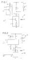
- FIG. 1 shows a conventional transmission stage which has the disadvantages mentioned of a conventional optoelectronic sensor.
- an optoelectronic transmitter element 10 comprising transmitter unit 12 on the one hand via a resistor 14 to the one, for example a positive one Terminal 16 having potential and on the other hand to the other, for example Ground corresponding terminal 18 of a supply voltage source 20 connected, which in the following case is a DC voltage source.
- a Transmit capacitor 24 connected in parallel.
- the transmission unit 12 is via a control circuit 26 leading to driver 22 can be driven.
- the aim of the invention is to provide an improved optoelectronic sensor to create the type mentioned, in which the aforementioned Disadvantages are eliminated.
- the use should also significantly smaller and cheaper components are made possible.
- the power loss should be reduced to a minimum and the Interference radiation via the supply line must be reduced.
- This object is achieved according to the invention in that one in dependence from the control of the display element and from the supply voltage level controllable circuit arrangement is provided, via the transmission unit and the display element when the display element is activated in the case of a supply voltage above a limit can be connected in series and in the case of a value below the limit or this corresponding supply voltage two to each other parallel circuits can be switched, the supply voltage in one case on the series circuit and in the other case on the two parallel circuits are present, and via the uncontrolled Display element the transmitter unit separately from the display element can be connected to the supply voltage.
- the circuit arrangement is an optoelectronic sensor Matrix switch formed. So an active switching matrix is used, whose switching state depends on the control of the display element and automatically from the supply voltage level accordingly changes.
- the transmission unit expediently comprises one with the transmission element drivers connected in series.
- the transmission capacitor is preferred to the series circuit containing the transmitting element and the driver connected in parallel.
- the power loss can be further reduced, for example, by that over the circuit arrangement at a limit Supply voltage another module such as one in particular Evaluation circuit (e.g. amplifier, signal processing, etc.) or the like with the display element and / or the transmitter unit in series is switchable.
- another module such as one in particular Evaluation circuit (e.g. amplifier, signal processing, etc.) or the like with the display element and / or the transmitter unit in series is switchable.
- Some AC devices already have a series connection of display and residual electronics applied. Since this is, however is always higher voltages (24-260 V AC voltage) the switching according to the invention described above is not necessary.
- the switchover according to the invention is not only for example halving the losses when a specified voltage is exceeded possible, it is also possible to reach the functional data secured at lower voltages.
- the circuit arrangement can be used to establish the respective connections advantageously at least one switchable current source and / or at least one switching element having a defined on-resistance include.
- the circuit arrangement with a voltage limitation is provided. This is preferably provided to the Voltage on at least one connected to the circuit arrangement Limit assembly. For example, it can limit serve the voltage applied to the transmitter unit.
- the respective voltage limitation can be a control circuit, for example include.
- a control circuit can, for example Power source are controlled so that at least at the beginning of each Activation of the transmitter unit on the transmitter capacitor a predeterminable Voltage is present.
- a respective voltage limitation can also be carried out in this way, for example be that the connection between a respective assembly and the supply voltage source is interrupted as soon as the on the Module applied voltage a defined, preferably adjustable Value exceeds.
- Fig. 2 shows a schematic partial representation of a purely exemplary embodiment an optoelectronic sensor 34 according to the invention, which is in particular a light barrier or the like can act.
- this optoelectronic sensor 34 comprises at least one a transmission unit 38 comprising an optoelectronic transmission element 36, at least one optoelectronic display element 40 and at least one Supply voltage source 42, here a DC voltage source.
- the switching state of the active matrix switch 44 changes depending on the control of the display element 40 and automatically from the supply voltage level so that via this matrix switch 44 when the display element 40 is activated the transmission unit 38 and the display element 40 in the case of one above one Limit value lying supply voltage 42 connected in series and in In the case of a value below or corresponding to the limit Supply voltage 42 two mutually parallel circuits a, b; c, d be switched on.
- the supply voltage 42 is in one Case on series circuit a, d and in the other case on the two to each other parallel circuits a, b; c, d an.
- the transmission unit 38 via the matrix switch 44 connected separately from the display element 40 to the supply voltage 42.
- the matrix switch 44 has four pins in the present case, which are internal connected or separated accordingly become.
- the transmission element formed, for example, by a light-emitting diode 40 is between the one having, for example, a positive potential Terminal 46 of the supply voltage source 42 and pin 1 of the Matrix switch 44 switched.
- the pin 2 of the matrix switch 44 is through the current path c directly to the terminal 46 of the supply voltage source 42 connected.
- the other terminal 48 of the supply voltage source 42 is present Drop to mass.
- Pin 3 of the switching matrix 44 is connected to ground via the current path b.
- the Pin 4 of the matrix switch 44 is connected to the transmitter unit 38, at the other end, current path d connected again to ground.
- the display 40 is via a control line leading to the matrix switch 44 50 controllable.
- the transmission unit 38 comprises a series-connected transmission element 32 Driver 52 and a transmission capacitor 54, which for Transmitting element 36 and the series circuit d 'containing driver 52 are connected in parallel is.
- the driver 52 assigned to the transmission element 36 is over a control line 56 can be controlled.
- connection matrix low supply voltage higher supply voltage display off Connection between: Pin2 and Pin4 Connection between: Pin2 and Pin4 Display Connection between: Pin2 and Pin4 Pin1 and Pin3 Connection between: Pin1 and Pin4
- the limit can be adjustable.
- the matrix switch 44 can be used to establish the respective connections for example at least one switchable current source and / or at least a switch element having a defined on-resistance include.
- the matrix switch can be equipped with a voltage limitation be provided.
- the voltage can be at least one be connected to the matrix switch 44 connected module.
- a corresponding voltage limitation for the voltage applied to the transmission unit 38 may be provided.
- the respective voltage limitation can be a control circuit, for example comprise, via which preferably a current source can be controlled is that at least at the beginning of a respective activation of the transmission unit 38 a predetermined voltage is present at the transmitting capacitor 54.
- the respective voltage limitation can also be implemented in this way, for example be that the connection between the assembly in question, for example the transmission unit 38, and the supply voltage source 42 is interrupted as soon as the voltage applied to the module exceeds a defined, preferably adjustable value.
Landscapes
- Control Of Indicators Other Than Cathode Ray Tubes (AREA)
- Electronic Switches (AREA)
- Light Receiving Elements (AREA)
- Photometry And Measurement Of Optical Pulse Characteristics (AREA)
Abstract
Description
- der reduzierte Stromripple, wodurch sichergetellt ist, daß der insbesondere bei Tantalkondensatoren kritische Stromwert nicht erreicht wird, und
- die auch im Einfehlerfall vorhandene Begrenzung der Strahlleistung der Sendediode.
- eine mehrfache Verwendung von Strömen durch eine entsprechende Reihenschaltung
- Begrenzung der Spannung an Baugruppen
- Strombegrenzung zur Erreichung der Einfehlerbedingung.
- Fig. 1
- eine schematische Darstellung einer herkömmlichen Sendestufe eines herkömmlichen optoelektronischen Sensors und
- Fig. 2
- eine schematische Darstellung einer Ausführungsform der Sendestufe mit zugeordneter Anzeige des erfindungsgemäßen optoelektronischen Sensors.
| niedrige Versorgungsspannung | höhere Versorgungsspannung | |
| Anzeige aus | Verbindung zwischen: Pin2 und Pin4 | Verbindung zwischen: Pin2 und Pin4 |
| Anzeige an | Verbindung zwischen: Pin2 und Pin4 Pin1 and Pin3 | Verbindung zwischen: Pin1 und Pin4 |
- 10
- optoelektronisches Sendeelement
- 12
- Sendeeinheit
- 14
- Widerstand
- 16
- Klemme
- 18
- Klemme
- 20
- Versorgungsspannungsquelle
- 22
- Treiber
- 24
- Sendekondensator
- 26
- Steuerleitung
- 28
- Anzeigeelement
- 30
- Treiber
- 32
- Steuerleitung
- 34
- optoelektronischer Sensor
- 36
- optoelektronisches Sendeelement
- 38
- Sendeeinheit
- 40
- optoelektronisches Anzeigeelement
- 42
- Versorgungsspannung, Versorgungsspannungsquelle
- 44
- Schaltungsanordnung, Matrixschalter
- 46
- Klemme
- 48
- Klemme
- 50
- Steuerleitung
- 52
- Treiber
- 54
- Sendekondensator
- 56
- Steuerleitung
- a, b, c, d
- Strompfade
- d'
- Serienkreis
Claims (14)
- Optoelektronischer Sensor (34), insbesondere Lichtschranke oder dergleichen, mit wenigstens einer ein optoelektronisches Sendeelement (36) umfassenden Sendeeinheit (38), wenigstens einem optoelektronischen Anzeigeelement (40) und wenigstens einer Versorgungsspannungsquelle (42),
dadurch gekennzeichnet, daß eine in Abhängigkeit von der Ansteuerung des Anzeigeelements (40) und von der Versorgungsspannungshöhe ansteuerbare Schaltungsanordnung (44) vorgesehen ist, über die bei angesteuertem Anzeigeelement (40) die Sendeeinheit (38) und das Anzeigeelement (40) im Fall einer über einem Grenzwert liegenden Versorgungsspannung (42) in Serie schaltbar und im Fall einer unter dem Grenzwert liegenden oder diesem entsprechenden Versorgungsspannung (42) zwei zueinander parallelen Stromkreisen (a, b; c, d) zuschaltbar sind, wobei die Versorgungsspannung im einen Fall am Serienkreis (a, d) und im andern Fall an den beiden zueinander parallelen Stromkreisen (a, b; c, d) anliegt, und über die bei nicht angesteuertem Anzeigeelement (40) die Sendeeinheit (38) getrennt vom Anzeigeelement (40) mit der Versorgungsspannung (42) verbindbar ist. - Sensor nach Anspruch 1,
dadurch gekennzeichnet, daß die Schaltungsanordnung durch einen Matrixschalter (44) gebildet ist. - Sensor nach einem der vorhergehenden Ansprüche,
dadurch gekennzeichnet, daß die Sendeeinheit (38) einen Sendekondensator (54) umfaßt, der zu einem das Sendeelement (36) enthaltenden Stromkreis (d') parallel geschaltet ist. - Sensor nach einem der vorhergehenden Ansprüche,
dadurch gekennzeichnet, daß die Sendeeinheit (38) einen mit dem Sendeelement (32) in Serie geschalteten Treiber (52) umfaßt. - Sensor nach Anspruch 3 und 4,
dadurch gekennzeichnet, daß der Sendekondensator (54) zu dem das Sendeelement (36) und den Treiber (52) enthaltenden Serienkreis (d') parallel geschaltet ist. - Sensor nach einem der vorhergehenden Ansprüchen,
dadurch gekennzeichnet, daß über die Schaltungsanordnung (44) bei über einem Grenzwert liegender Versorgungsspannung (42) eine weitere Baugruppe wie insbesondere eine Auswerteschaltung oder dergleichen mit dem Anzeigeelement (40) und/oder der Sendeeinheit (38) in Serie schaltbar ist. - Sensor nach einem der vorhergehenden Ansprüche,
dadurch gekennzeichnet, daß der Grenzwert einstellbar ist. - Sensor nach einem der vorhergehenden Ansprüchen,
dadurch gekennzeichnet, daß die Schaltungsanordnung (44) zur Herstellung der jeweiligen Verbindungen wenigstens eine schaltbare Stromquelle umfaßt. - Sensor nach einem der vorhergehenden Ansprüchen,
dadurch gekennzeichnet, daß die Schaltungsanordnung (44) zur Herstellung der jeweiligen Verbindungen wenigstens ein einen definierten Einschaltwiderstand besitzendes Schalterelement umfaßt. - Sensor nach einem der vorhergehenden Ansprüchen,
dadurch gekennzeichnet, daß die Schaltungsanordnung (44) mit einer Spannungsbegrenzung versehen ist. - Sensor nach Anspruch 10,
dadurch gekennzeichnet, daß die Spannungsbegrenzung vorgesehen ist, um die Spannung an wenigstens einer an die Schaltungsanordnung (44) angeschlossenen Baugruppe (38) zu begrenzen. - Sensor nach Anspruch 13,
dadurch gekennzeichnet, daß zumindest zur Begrenzung der an der Sendeeinheit (38) anliegenden Spannung eine entsprechende Spannungsbegrenzung vorgesehen ist. - Sensor nach Anspruch 12,
dadurch gekennzeichnet, daß die Spannungsbegrenzung eine Regelschaltung umfaßt, über die vorzugsweise eine Stromquelle so ansteuerbar ist, daß zumindest zu Beginn einer jeweiligen Ansteuerung der Sendeeinheit (38) am Sendekondensator (54) eine vorgebbare Spannung anliegt. - Sensor nach einem der vorhergehenden Ansprüche,
dadurch gekennzeichnet, daß die Spannungsbegrenzung so ausgeführt ist, daß die Verbindung zwischen einer jeweiligen Baugruppe (38) und der Versorgungsspannungsquelle (42) unterbrochen wird, sobald die an der Baugruppe (38) anliegende Spannung einen definierten, vorzugsweise einstellbaren Wert überschreitet.
Applications Claiming Priority (2)
| Application Number | Priority Date | Filing Date | Title |
|---|---|---|---|
| DE10032840A DE10032840A1 (de) | 2000-07-06 | 2000-07-06 | Optoelektronischer Sensor |
| DE10032840 | 2000-07-06 |
Publications (3)
| Publication Number | Publication Date |
|---|---|
| EP1170600A2 true EP1170600A2 (de) | 2002-01-09 |
| EP1170600A3 EP1170600A3 (de) | 2004-05-12 |
| EP1170600B1 EP1170600B1 (de) | 2006-11-02 |
Family
ID=7647989
Family Applications (1)
| Application Number | Title | Priority Date | Filing Date |
|---|---|---|---|
| EP01114374A Expired - Lifetime EP1170600B1 (de) | 2000-07-06 | 2001-06-13 | Optoelektronischer Sensor |
Country Status (3)
| Country | Link |
|---|---|
| EP (1) | EP1170600B1 (de) |
| AT (1) | ATE344465T1 (de) |
| DE (2) | DE10032840A1 (de) |
Family Cites Families (8)
| Publication number | Priority date | Publication date | Assignee | Title |
|---|---|---|---|---|
| DE2340978A1 (de) * | 1973-08-14 | 1975-02-27 | Licentia Gmbh | Sender fuer wechsellichtschranke |
| US4247765A (en) * | 1979-01-03 | 1981-01-27 | Bergstroem Arne | Pulsed feedback circuit for an optoelectronic detector |
| US5091640A (en) * | 1991-06-24 | 1992-02-25 | Square D Company | Phase advance for ambient light suppression in phototransistors |
| DE4228112C1 (en) * | 1992-08-25 | 1993-07-01 | Leuze Electronic Gmbh + Co, 7311 Owen, De | Object detection arrangement - contains light source and receiver, comparator with comparison voltages controlled by micro-controller |
| DE4238666C2 (de) * | 1992-11-17 | 1994-11-24 | Leuze Electronic Gmbh & Co | Mit einem Sender und einem Empfänger ausgerüstete Einrichtung zum Erfassen von Objekten |
| FR2723286B1 (fr) * | 1994-07-29 | 1996-09-13 | Vibrachoc Sa | Circuit de montage de diodes electroluminescentes |
| DE19530601A1 (de) * | 1995-08-21 | 1997-02-27 | Nsm Ag | Vorrichtung zur Funktionskontrolle von Lichtschranken |
| DE19800553C2 (de) * | 1997-01-18 | 2003-07-31 | Leuze Electronic Gmbh & Co | Optoelektronische Vorrichtung |
-
2000
- 2000-07-06 DE DE10032840A patent/DE10032840A1/de not_active Withdrawn
-
2001
- 2001-06-13 AT AT01114374T patent/ATE344465T1/de not_active IP Right Cessation
- 2001-06-13 EP EP01114374A patent/EP1170600B1/de not_active Expired - Lifetime
- 2001-06-13 DE DE50111346T patent/DE50111346D1/de not_active Expired - Lifetime
Also Published As
| Publication number | Publication date |
|---|---|
| EP1170600B1 (de) | 2006-11-02 |
| DE50111346D1 (de) | 2006-12-14 |
| EP1170600A3 (de) | 2004-05-12 |
| DE10032840A1 (de) | 2002-01-17 |
| ATE344465T1 (de) | 2006-11-15 |
Similar Documents
| Publication | Publication Date | Title |
|---|---|---|
| EP1074081B1 (de) | Verpolschutzschaltung | |
| EP0572706B1 (de) | Ansteuerschaltung für einen Leistungs-FET mit sourceseitiger Last | |
| EP3317964B1 (de) | Hochfrequenzverstärkeranordnung | |
| DE69311823T2 (de) | Differentieller Diskriminator mit dualer Schwelle | |
| EP2564671B1 (de) | Spannungsfeste schnittstellenschaltung | |
| DE3138645C2 (de) | ||
| DE102006036569B4 (de) | Treiberschaltung eines Halbleiter-Leistungsschaltelementes | |
| DE19631751C1 (de) | Ansteuerschaltung für einen Leistungs-FET mit sourceseitiger Last | |
| EP1170600B1 (de) | Optoelektronischer Sensor | |
| DE102004044114B4 (de) | Videoeingangsschutzschaltung zum Schutz gegen Kurzschluss zur Batterie unter Beibehaltung eines Abschlusswiderstands | |
| DE10349629B4 (de) | Elektronischer Schaltkreis | |
| EP0489935B1 (de) | MOSFET-Schalter für eine induktive Last | |
| EP0696849A2 (de) | Steuergerät mit einer Schaltungsanordnung zum Schutz des Steuergerätes bei Unterbrechung der Steuergerätemasse | |
| DE102010028448A1 (de) | Schnittstellenschaltung und Verfahren zur Beeinflussung der Flankensteilheit eines Ansteuersignals | |
| DE102013213042B4 (de) | Elektronische Schaltungsanordnung zur Verwendung in einem explosionsgefährdeten Bereich | |
| EP3506723B1 (de) | Schaltwandler zum speisen einer led-serienschaltung | |
| EP1193824A2 (de) | Gegenspannungsschutzschaltung | |
| DE3632741C2 (de) | ||
| DE19937682A1 (de) | Elektrische Schaltungsanordnung | |
| DE202010006269U1 (de) | Spannungsfeste Schnittstellenschaltung | |
| DE102024133711A1 (de) | Beleuchtungsvorrichtung für ein Lichtlaufzeitkamerasystem | |
| DE19511199A1 (de) | Schaltungsanordnung zum Schalten einer elektrischen Last | |
| DE102017131200B4 (de) | Digitale Eingangsschaltung zum Empfangen digitaler Eingangssignale eines Signalgebers | |
| WO2018073229A1 (de) | Verfahren zum regeln eines betriebsstroms einer leuchteinheit sowie steuergerät und kraftfahrzeug | |
| EP1280384A2 (de) | Dimm-Modul |
Legal Events
| Date | Code | Title | Description |
|---|---|---|---|
| PUAI | Public reference made under article 153(3) epc to a published international application that has entered the european phase |
Free format text: ORIGINAL CODE: 0009012 |
|
| AK | Designated contracting states |
Kind code of ref document: A2 Designated state(s): AT BE CH CY DE DK ES FI FR GB GR IE IT LI LU MC NL PT SE TR |
|
| AX | Request for extension of the european patent |
Free format text: AL;LT;LV;MK;RO;SI |
|
| PUAL | Search report despatched |
Free format text: ORIGINAL CODE: 0009013 |
|
| AK | Designated contracting states |
Kind code of ref document: A3 Designated state(s): AT BE CH CY DE DK ES FI FR GB GR IE IT LI LU MC NL PT SE TR |
|
| AX | Request for extension of the european patent |
Extension state: AL LT LV MK RO SI |
|
| RIC1 | Information provided on ipc code assigned before grant |
Ipc: 7G 01V 8/12 A Ipc: 7G 01V 8/10 B |
|
| 17P | Request for examination filed |
Effective date: 20040706 |
|
| AKX | Designation fees paid |
Designated state(s): AT BE CH CY DE DK ES FI FR GB GR IE IT LI LU MC NL PT SE TR |
|
| GRAP | Despatch of communication of intention to grant a patent |
Free format text: ORIGINAL CODE: EPIDOSNIGR1 |
|
| GRAS | Grant fee paid |
Free format text: ORIGINAL CODE: EPIDOSNIGR3 |
|
| GRAA | (expected) grant |
Free format text: ORIGINAL CODE: 0009210 |
|
| AK | Designated contracting states |
Kind code of ref document: B1 Designated state(s): AT BE CH CY DE DK ES FI FR GB GR IE IT LI LU MC NL PT SE TR |
|
| PG25 | Lapsed in a contracting state [announced via postgrant information from national office to epo] |
Ref country code: NL Free format text: LAPSE BECAUSE OF FAILURE TO SUBMIT A TRANSLATION OF THE DESCRIPTION OR TO PAY THE FEE WITHIN THE PRESCRIBED TIME-LIMIT Effective date: 20061102 Ref country code: FI Free format text: LAPSE BECAUSE OF FAILURE TO SUBMIT A TRANSLATION OF THE DESCRIPTION OR TO PAY THE FEE WITHIN THE PRESCRIBED TIME-LIMIT Effective date: 20061102 Ref country code: IE Free format text: LAPSE BECAUSE OF FAILURE TO SUBMIT A TRANSLATION OF THE DESCRIPTION OR TO PAY THE FEE WITHIN THE PRESCRIBED TIME-LIMIT Effective date: 20061102 Ref country code: IT Free format text: LAPSE BECAUSE OF FAILURE TO SUBMIT A TRANSLATION OF THE DESCRIPTION OR TO PAY THE FEE WITHIN THE PRESCRIBED TIME-LIMIT;WARNING: LAPSES OF ITALIAN PATENTS WITH EFFECTIVE DATE BEFORE 2007 MAY HAVE OCCURRED AT ANY TIME BEFORE 2007. THE CORRECT EFFECTIVE DATE MAY BE DIFFERENT FROM THE ONE RECORDED. Effective date: 20061102 |
|
| REG | Reference to a national code |
Ref country code: GB Ref legal event code: FG4D Free format text: NOT ENGLISH |
|
| REG | Reference to a national code |
Ref country code: IE Ref legal event code: FG4D Free format text: LANGUAGE OF EP DOCUMENT: GERMAN |
|
| REG | Reference to a national code |
Ref country code: CH Ref legal event code: EP |
|
| REF | Corresponds to: |
Ref document number: 50111346 Country of ref document: DE Date of ref document: 20061214 Kind code of ref document: P |
|
| PG25 | Lapsed in a contracting state [announced via postgrant information from national office to epo] |
Ref country code: DK Free format text: LAPSE BECAUSE OF FAILURE TO SUBMIT A TRANSLATION OF THE DESCRIPTION OR TO PAY THE FEE WITHIN THE PRESCRIBED TIME-LIMIT Effective date: 20070202 Ref country code: SE Free format text: LAPSE BECAUSE OF FAILURE TO SUBMIT A TRANSLATION OF THE DESCRIPTION OR TO PAY THE FEE WITHIN THE PRESCRIBED TIME-LIMIT Effective date: 20070202 |
|
| PG25 | Lapsed in a contracting state [announced via postgrant information from national office to epo] |
Ref country code: ES Free format text: LAPSE BECAUSE OF FAILURE TO SUBMIT A TRANSLATION OF THE DESCRIPTION OR TO PAY THE FEE WITHIN THE PRESCRIBED TIME-LIMIT Effective date: 20070213 |
|
| RAP2 | Party data changed (patent owner data changed or rights of a patent transferred) |
Owner name: SICK AG |
|
| NLT2 | Nl: modifications (of names), taken from the european patent patent bulletin |
Owner name: SICK AG Effective date: 20070214 |
|
| PG25 | Lapsed in a contracting state [announced via postgrant information from national office to epo] |
Ref country code: PT Free format text: LAPSE BECAUSE OF FAILURE TO SUBMIT A TRANSLATION OF THE DESCRIPTION OR TO PAY THE FEE WITHIN THE PRESCRIBED TIME-LIMIT Effective date: 20070402 |
|
| ET | Fr: translation filed | ||
| NLV1 | Nl: lapsed or annulled due to failure to fulfill the requirements of art. 29p and 29m of the patents act | ||
| GBV | Gb: ep patent (uk) treated as always having been void in accordance with gb section 77(7)/1977 [no translation filed] |
Effective date: 20061102 |
|
| REG | Reference to a national code |
Ref country code: IE Ref legal event code: FD4D |
|
| PLBE | No opposition filed within time limit |
Free format text: ORIGINAL CODE: 0009261 |
|
| STAA | Information on the status of an ep patent application or granted ep patent |
Free format text: STATUS: NO OPPOSITION FILED WITHIN TIME LIMIT |
|
| 26N | No opposition filed |
Effective date: 20070803 |
|
| PG25 | Lapsed in a contracting state [announced via postgrant information from national office to epo] |
Ref country code: GB Free format text: LAPSE BECAUSE OF FAILURE TO SUBMIT A TRANSLATION OF THE DESCRIPTION OR TO PAY THE FEE WITHIN THE PRESCRIBED TIME-LIMIT Effective date: 20061102 |
|
| BERE | Be: lapsed |
Owner name: SICK A.G. Effective date: 20070630 |
|
| PG25 | Lapsed in a contracting state [announced via postgrant information from national office to epo] |
Ref country code: MC Free format text: LAPSE BECAUSE OF NON-PAYMENT OF DUE FEES Effective date: 20070630 |
|
| PG25 | Lapsed in a contracting state [announced via postgrant information from national office to epo] |
Ref country code: BE Free format text: LAPSE BECAUSE OF NON-PAYMENT OF DUE FEES Effective date: 20070630 |
|
| PG25 | Lapsed in a contracting state [announced via postgrant information from national office to epo] |
Ref country code: GR Free format text: LAPSE BECAUSE OF FAILURE TO SUBMIT A TRANSLATION OF THE DESCRIPTION OR TO PAY THE FEE WITHIN THE PRESCRIBED TIME-LIMIT Effective date: 20070203 |
|
| PG25 | Lapsed in a contracting state [announced via postgrant information from national office to epo] |
Ref country code: AT Free format text: LAPSE BECAUSE OF NON-PAYMENT OF DUE FEES Effective date: 20070613 |
|
| PG25 | Lapsed in a contracting state [announced via postgrant information from national office to epo] |
Ref country code: CY Free format text: LAPSE BECAUSE OF FAILURE TO SUBMIT A TRANSLATION OF THE DESCRIPTION OR TO PAY THE FEE WITHIN THE PRESCRIBED TIME-LIMIT Effective date: 20061102 Ref country code: LU Free format text: LAPSE BECAUSE OF NON-PAYMENT OF DUE FEES Effective date: 20070613 |
|
| PG25 | Lapsed in a contracting state [announced via postgrant information from national office to epo] |
Ref country code: TR Free format text: LAPSE BECAUSE OF FAILURE TO SUBMIT A TRANSLATION OF THE DESCRIPTION OR TO PAY THE FEE WITHIN THE PRESCRIBED TIME-LIMIT Effective date: 20061102 |
|
| PGFP | Annual fee paid to national office [announced via postgrant information from national office to epo] |
Ref country code: CH Payment date: 20130621 Year of fee payment: 13 |
|
| PGFP | Annual fee paid to national office [announced via postgrant information from national office to epo] |
Ref country code: IT Payment date: 20130624 Year of fee payment: 13 Ref country code: FR Payment date: 20130703 Year of fee payment: 13 |
|
| REG | Reference to a national code |
Ref country code: CH Ref legal event code: PL |
|
| REG | Reference to a national code |
Ref country code: FR Ref legal event code: ST Effective date: 20150227 |
|
| PG25 | Lapsed in a contracting state [announced via postgrant information from national office to epo] |
Ref country code: CH Free format text: LAPSE BECAUSE OF NON-PAYMENT OF DUE FEES Effective date: 20140630 Ref country code: IT Free format text: LAPSE BECAUSE OF NON-PAYMENT OF DUE FEES Effective date: 20140613 Ref country code: LI Free format text: LAPSE BECAUSE OF NON-PAYMENT OF DUE FEES Effective date: 20140630 |
|
| PG25 | Lapsed in a contracting state [announced via postgrant information from national office to epo] |
Ref country code: FR Free format text: LAPSE BECAUSE OF NON-PAYMENT OF DUE FEES Effective date: 20140630 |
|
| PGFP | Annual fee paid to national office [announced via postgrant information from national office to epo] |
Ref country code: DE Payment date: 20190624 Year of fee payment: 19 |
|
| REG | Reference to a national code |
Ref country code: DE Ref legal event code: R119 Ref document number: 50111346 Country of ref document: DE |
|
| PG25 | Lapsed in a contracting state [announced via postgrant information from national office to epo] |
Ref country code: DE Free format text: LAPSE BECAUSE OF NON-PAYMENT OF DUE FEES Effective date: 20210101 |