EP1168034A2 - Beleuchtungseinrichtung und Koordinaten-Messgerät mit einer Beleuchtungseinrichtung - Google Patents
Beleuchtungseinrichtung und Koordinaten-Messgerät mit einer Beleuchtungseinrichtung Download PDFInfo
- Publication number
- EP1168034A2 EP1168034A2 EP01114954A EP01114954A EP1168034A2 EP 1168034 A2 EP1168034 A2 EP 1168034A2 EP 01114954 A EP01114954 A EP 01114954A EP 01114954 A EP01114954 A EP 01114954A EP 1168034 A2 EP1168034 A2 EP 1168034A2
- Authority
- EP
- European Patent Office
- Prior art keywords
- optics
- light
- fiber bundle
- optical
- illumination
- Prior art date
- Legal status (The legal status is an assumption and is not a legal conclusion. Google has not performed a legal analysis and makes no representation as to the accuracy of the status listed.)
- Granted
Links
- 238000005286 illumination Methods 0.000 title claims abstract description 40
- 239000000835 fiber Substances 0.000 claims abstract description 30
- 239000013307 optical fiber Substances 0.000 claims abstract description 30
- 230000008878 coupling Effects 0.000 claims abstract description 25
- 238000010168 coupling process Methods 0.000 claims abstract description 25
- 238000005859 coupling reaction Methods 0.000 claims abstract description 25
- 238000009826 distribution Methods 0.000 claims abstract description 18
- 238000000265 homogenisation Methods 0.000 claims abstract description 18
- 239000000758 substrate Substances 0.000 claims abstract description 4
- 230000003287 optical effect Effects 0.000 claims description 46
- VYPSYNLAJGMNEJ-UHFFFAOYSA-N silicon dioxide Inorganic materials O=[Si]=O VYPSYNLAJGMNEJ-UHFFFAOYSA-N 0.000 description 12
- 239000010453 quartz Substances 0.000 description 11
- 238000005259 measurement Methods 0.000 description 6
- 239000010438 granite Substances 0.000 description 5
- 241001270131 Agaricus moelleri Species 0.000 description 4
- 230000001419 dependent effect Effects 0.000 description 4
- 238000010586 diagram Methods 0.000 description 4
- 238000007689 inspection Methods 0.000 description 3
- 238000004519 manufacturing process Methods 0.000 description 3
- 239000000523 sample Substances 0.000 description 3
- 238000003491 array Methods 0.000 description 2
- 230000003247 decreasing effect Effects 0.000 description 2
- 238000003384 imaging method Methods 0.000 description 2
- 238000000034 method Methods 0.000 description 2
- 230000005855 radiation Effects 0.000 description 2
- 239000004065 semiconductor Substances 0.000 description 2
- TVEXGJYMHHTVKP-UHFFFAOYSA-N 6-oxabicyclo[3.2.1]oct-3-en-7-one Chemical compound C1C2C(=O)OC1C=CC2 TVEXGJYMHHTVKP-UHFFFAOYSA-N 0.000 description 1
- 238000013459 approach Methods 0.000 description 1
- 230000008901 benefit Effects 0.000 description 1
- 238000009529 body temperature measurement Methods 0.000 description 1
- 238000010894 electron beam technology Methods 0.000 description 1
- 238000005530 etching Methods 0.000 description 1
- 239000013305 flexible fiber Substances 0.000 description 1
- 239000002241 glass-ceramic Substances 0.000 description 1
- 210000003128 head Anatomy 0.000 description 1
- 238000001459 lithography Methods 0.000 description 1
- 238000012986 modification Methods 0.000 description 1
- 230000004048 modification Effects 0.000 description 1
- 238000012856 packing Methods 0.000 description 1
- 238000002360 preparation method Methods 0.000 description 1
- 230000008569 process Effects 0.000 description 1
- 210000001747 pupil Anatomy 0.000 description 1
- 230000003595 spectral effect Effects 0.000 description 1
- 238000003892 spreading Methods 0.000 description 1
- 230000007480 spreading Effects 0.000 description 1
- 230000004304 visual acuity Effects 0.000 description 1
Images




Classifications
-
- G—PHYSICS
- G03—PHOTOGRAPHY; CINEMATOGRAPHY; ANALOGOUS TECHNIQUES USING WAVES OTHER THAN OPTICAL WAVES; ELECTROGRAPHY; HOLOGRAPHY
- G03F—PHOTOMECHANICAL PRODUCTION OF TEXTURED OR PATTERNED SURFACES, e.g. FOR PRINTING, FOR PROCESSING OF SEMICONDUCTOR DEVICES; MATERIALS THEREFOR; ORIGINALS THEREFOR; APPARATUS SPECIALLY ADAPTED THEREFOR
- G03F7/00—Photomechanical, e.g. photolithographic, production of textured or patterned surfaces, e.g. printing surfaces; Materials therefor, e.g. comprising photoresists; Apparatus specially adapted therefor
- G03F7/70—Microphotolithographic exposure; Apparatus therefor
- G03F7/70058—Mask illumination systems
-
- G—PHYSICS
- G01—MEASURING; TESTING
- G01B—MEASURING LENGTH, THICKNESS OR SIMILAR LINEAR DIMENSIONS; MEASURING ANGLES; MEASURING AREAS; MEASURING IRREGULARITIES OF SURFACES OR CONTOURS
- G01B11/00—Measuring arrangements characterised by the use of optical techniques
- G01B11/002—Measuring arrangements characterised by the use of optical techniques for measuring two or more coordinates
- G01B11/005—Measuring arrangements characterised by the use of optical techniques for measuring two or more coordinates coordinate measuring machines
-
- G—PHYSICS
- G02—OPTICS
- G02B—OPTICAL ELEMENTS, SYSTEMS OR APPARATUS
- G02B27/00—Optical systems or apparatus not provided for by any of the groups G02B1/00 - G02B26/00, G02B30/00
- G02B27/09—Beam shaping, e.g. changing the cross-sectional area, not otherwise provided for
-
- G—PHYSICS
- G02—OPTICS
- G02B—OPTICAL ELEMENTS, SYSTEMS OR APPARATUS
- G02B6/00—Light guides; Structural details of arrangements comprising light guides and other optical elements, e.g. couplings
- G02B6/24—Coupling light guides
- G02B6/42—Coupling light guides with opto-electronic elements
- G02B6/4298—Coupling light guides with opto-electronic elements coupling with non-coherent light sources and/or radiation detectors, e.g. lamps, incandescent bulbs, scintillation chambers
-
- G—PHYSICS
- G02—OPTICS
- G02B—OPTICAL ELEMENTS, SYSTEMS OR APPARATUS
- G02B6/00—Light guides; Structural details of arrangements comprising light guides and other optical elements, e.g. couplings
- G02B6/0001—Light guides; Structural details of arrangements comprising light guides and other optical elements, e.g. couplings specially adapted for lighting devices or systems
Definitions
- the invention relates to a lighting device with the features of The preamble of independent claim 1.
- the invention further relates to a Coordinate measuring device with a lighting device with the features the preamble of independent claim 5.
- Lighting devices are known which are used to generate a homogeneous light field work with an optical fiber.
- Such Illumination device is, for example, in the coordinate measuring machine Leica® LMS IPRO from Leica Microsystems GmbH is used.
- a 100W Hg-Xe discharge lamp is used as the light source.
- Over a Coupling optics are then created using a tube lens and a PLAN-APO 50x objective illuminates the sample in a known Köhler way. With this Illumination device is an image field with a diameter of Illuminated 0.056 mm.
- the known lighting device has the advantage that the Light source, which is also a strong heat source, far outside of the actual measurement location or far from the sample to be measured can be arranged. This will affect the temperature Measurement accuracy of the coordinate measuring machine minimized. At the same time it will Illumination light via the flexible fiber optic cable to anyone Measurement site.
- the disadvantage of the known lighting device is that due to the Beam pattern of multimode fibers the angular range in which the Intensity of the emitted light only in the order of a few Percent varies, is very narrow.
- the fiber diameter must be correspondingly large be dimensioned.
- the stiffness of optical fibers increases with it increasing diameter strongly.
- a homogeneously illuminated image field of the Size 0.35 mm required. This would require an optical fiber with one Core diameters larger than 1 mm can be used to ensure adequate Achieve homogeneity in the image field. Fibers with a core diameter However, due to their rigidity, they are no longer larger than 1 mm in practice used.
- the differences in brightness in the illuminated image field should be very be small.
- the lighting device according to the invention in turn uses one Optical fiber.
- holographic lenses can be used as homogenization optics Optical Elements (HOE), Diffractive Optical Elements (DOE), Honeycomb condensers or combinations of lens arrays and Spreading discs are used.
- HOE homogenization optics Optical Elements
- DOE Diffractive Optical Elements
- Honeycomb condensers or combinations of lens arrays and Spreading discs are used.
- micro honeycomb condenser consists of two quartz plates cemented together, each on the outer surfaces have dense array of plano-convex microlenses, the two External surfaces alternately in the focal plane of the microlenses on each opposite outer surface.
- the differences in brightness be very small in the illuminated image field.
- a fiber bundle consisting of many individual fibers can be used. This type of fiber has low rigidity even with a large diameter.
- the radiation characteristic of individual fibers is strongly dependent on the state of curvature Fiber dependent, which requires a greater adjustment effort. fiber bundles are significantly less sensitive to curvature.
- the Light balance i.e. the quotient of the total intensity in the image field Intensity of the light emitted by the fiber when homogenized comparatively cheapest with a lens array.
- a homogeneous Illuminated image field with a minimum diameter of 0.35 mm achieved a numerical aperture of 0.60.
- the lighting inhomogeneity is less than ⁇ 2% of the mean between the maximum intensity and the minimum intensity.
- a coordinate measuring machine In a coordinate measuring machine according to the invention, with the structures of Lithography masks of the semiconductor industry are measured, that is homogeneously illuminated image field is the same size. This is for example refocusing on changes in the situation of the Structural levels due to the manufacturing-related mask thickness tolerances occur, not necessary. Here, too, is Illumination inhomogeneity less than ⁇ 2% of the mean between the Maximum intensity and minimum intensity. This leads to a clear one Improved measurement accuracy, especially with large masks.
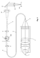
- FIG. 1 shows the optical diagram of an illumination device according to the invention, here specifically for transmitted light illumination, as can be used, for example, in a coordinate measuring machine or a stepper.
- a transmitted-light illumination beam path goes along from a light source 1 an optical axis 2.
- An optical fiber bundle 4 is used as the optical waveguide used.
- the homogenization optics 6 consist of a micro honeycomb condenser 7 and a lens member 8, which the Exit opening 9 of the fiber bundle 4 in an intermediate image plane 10 overlay a homogeneous intermediate image.
- FIG. 2 shows an enlarged detail of the area designated by "X" in FIG. 1 .
- a section through a micro-honeycomb condenser 7 is shown.
- the front outer surface 11 of the micro-honeycomb condenser 7 (arranged on the left in the figure) is located in the focal plane of the decoupling optics 5.
- the micro-honeycomb condenser 7 consists of a first, flat quartz plate 11 and a second, flat quartz plate 12, both cemented together.
- the putty surface 14 between the first quartz plate 11 and the second Quartz plate 12 is shown disproportionately thick.
- the outer surface 13 of the first quartz plate 11 represents the front of the Micro honeycomb condenser 7, to which the coupling-out optics 5 coming light hits.
- the outer surface 15 of the second quartz plate 12 provides the back of the micro honeycomb condenser 7 through which the light emerges again.
- the second quartz plate 12 are plano-concave in a hexagonal arrangement Microlenses (positive lenses) 16 etched.
- the etching can for example using a lithographic process.
- the two Outer surfaces 13 and 15 are mutually in the focus of each other microlenses arranged opposite each outer surface 13, 15 16th
- micro-honeycomb condenser 7 Multiple images of the outlet opening 9 of the fiber bundle 4.
- the number of Multiple images correspond to the number of illuminated microlenses 16.
- the size of the multiple images is determined from the focal length ratio of the Achromatic lenses 5 and the focal lengths of the microlenses 16.
- the further beam path is shown again in FIG. 1 .
- the lens element 8 which is preferably designed as an achromatic lens, then forms the cross sections of the microlenses 16 on the front outer surface 13 of the micro-honeycomb condenser 7 one above the other in an intermediate image plane 10. If the number of microlenses 16 has been chosen large enough, this superimposition ensures a very homogeneous intermediate image.
- the transmitted light object 18 can, for example, do this Measuring field of a coordinate measuring machine or a preparation on one Be microscopic.
- FIG 3 shows the optical diagram of an illumination device according to the invention, here specifically for incident light illumination, as can be used, for example, in a coordinate measuring machine or a stepper.
- a reflected-light illumination beam path with a goes from a light source 1 optical axis 2.
- An optical fiber bundle 4 is used as the optical waveguide used.
- the inhomogeneous intensity distribution remains the same Receive fiber bundle 4 emitted light. Therefore, the collimated light on Output of the decoupling optics 5 according to the invention to a Micro-honeycomb condenser 7 directed, which is part of a homogenization optics 6, which converts the inhomogeneous intensity distribution into a so-called "flat-top distribution" (so-called Super Gauss) transformed.
- micro-honeycomb condenser 7 On the back surface of the micro-honeycomb condenser 7, one then obtains how already described, multiple images of the light source, in this case the exit opening 9 of the fiber bundle 4.
- the number of multiple images corresponds to the number of illuminated microlenses 16.
- a lens element 8 which is preferably designed as an achromatic lens, forms then the cross sections of the microlenses 16 on the front outer surface 13 of the micro-honeycomb condenser 7 from one another into an intermediate image plane 10. This overlay ensures if the number of microlenses 16 is large enough was chosen for a homogeneous intermediate image.
- the incident light object 22 can, for example, be a measuring field of a Coordinate measuring device or a specimen on a microscope stage.
- FIG. 4 shows an exemplary embodiment of a coordinate measuring machine with a combined incident light and transmitted light illumination, which comprises a transmitted light illumination device according to the invention.
- the coordinate measuring device shown has a granite block 23 which is mounted on vibration dampers 24, 25.
- a measuring table 26 formed as a frame on air bearings 27, 28 in the x and y directions (indicated by two arrows in the drawing) sliding displaceable.
- the frame of the measuring table 26 advantageously consists of a glass ceramic with a low coefficient of thermal expansion.
- the Drive elements for moving the measuring table 26 are not shown.
- the position of the measuring table 26 is determined using a laser interferometer system 29 measured in the x and y directions.
- a mask 30 is inserted into the frame of the measuring table 26.
- the mask 30 is e.g. made of quartz glass. Structures 31 are on the mask surface applied. Since the measuring table 26 is designed as a frame, the Mask 30 can also be illuminated from below.
- a lens 20 is located above the mask 30 as an imaging system high optical quality, which for focusing along its optical axis 2 in z direction is adjustable.
- the divider mirror 32 Light from an incident light light source 33 is introduced into the optical beam path and on the other hand the imaging beams are applied to a detector device 34 steered.
- the detector device 34 is e.g. a CCD camera with high-resolution pixel array.
- the incident light light source 33 emits for example in the near UV spectral range. By means of the detector device 34 becomes the position of a structure 31 as coordinates on the mask 30 certainly.
- a transmitted light illumination device as a further illumination device with a height-adjustable condenser 17 and a light source 1 used.
- a transmitted light illumination beam path goes from the light source 1 with an optical axis 2.
- the recorded light is with the Coupling optics 3 are coupled into an optical waveguide. As an optical fiber an optical fiber bundle 4 is used.
- the homogenization optics 6 consist of a micro honeycomb condenser 7 and a lens member 8, which the Exit opening 9 of the fiber bundle 4 in an intermediate image plane 10 overlay a homogeneous intermediate image.
- the Homogenization optics can also have large differences in intensity occur due to the large numerical aperture of the coupling optics be homogenized well. The remaining lighting inhomogeneity is only less than ⁇ 2% of the mean value between the maximum intensity and the minimum intensity. This leads to a clear one Improving the measurement accuracy of the coordinates of the structures 31, especially with large masks 30.
- the optical axis of the condenser 17 is aligned with the optical axis 2 of the Lens 20.
- the height adjustment of the condenser 17 is used for adjustment of the illuminating beams to be directed onto the structure 31 different optical thicknesses of masks 30.
- the condenser head can extend particularly into the open part of the measuring table frame. To the Protection against damage when the measuring table 26 moves condenser 26 can also cover the entire mask area Surface of the granite block 23 are drawn. Light sources 1 and 33 can be switched on independently of each other.
- the condenser 17 is shown with an optical axis 2.
- the intermediate image plane 10 is shown for orientation.
- the condenser 17 has moved close to a mask 30 on the open frame of a measuring table 26 is mounted. At the condenser 17th The upper side 35 facing away from the mask 30 has structures 31. This The top 35 of the mask 30 is covered with a certain image field homogeneous light intensity illuminated.
- the homogeneously illuminated image field has, for example, a minimum diameter of 0.35 mm at a numerical aperture from 0.60.
- a thicker mask 30 'with an upper side 35' is also dashed. located. Your top 35 'is significantly further from the condenser away. Because the lighting device has very large homogeneous image fields achieved, is also sufficient for the thicker mask 30 'for the position of the upper side 35 ', which determines the position of the structure planes, the image field for one Measurement still off. This results in refocusing Changes in the location of the structural levels as a result of manufacturing-related thickness tolerances of the masks do not occur.
Landscapes
- Physics & Mathematics (AREA)
- General Physics & Mathematics (AREA)
- Optics & Photonics (AREA)
- Microscoopes, Condenser (AREA)
- Length Measuring Devices By Optical Means (AREA)
- Exposure And Positioning Against Photoresist Photosensitive Materials (AREA)
- Exposure Of Semiconductors, Excluding Electron Or Ion Beam Exposure (AREA)
- Investigating Materials By The Use Of Optical Means Adapted For Particular Applications (AREA)
- Investigating Or Analysing Materials By Optical Means (AREA)
Abstract
Description
- Fig. 1:
- Optikschema einer Beleuchtungseinrichtung für eine Durchlicht-Beleuchtung;
- Fig. 2:
- Detailvergrößerung "X" aus Fig. 1, Schnitt durch einen Wabenkondensor;
- Fig. 3 :
- Optikschema einer Beleuchtungseinrichtung für eine Auflicht-Beleuchtung;
- Fig. 4:
- ein Koordinaten-Messgerät mit einer einer kombinierten Auflicht- und Durchlicht-Beleuchtung, welche eine erfindungsgemäße Durchlicht-Beleuchtungseinrichtung umfasst;
- Fig. 5:
- schematischer Strahlengang vor und nach dem Kondensor der Durchlicht-Beleuchtungseinrichtung aus Fig. 4 für unterschiedlich dicke Masken.
- 1.
- Lichtquelle
- 2.
- optische Achse
- 3.
- Einkoppeloptik
- 4.
- optisches Faserbündel
- 5.
- Auskoppeloptik
- 6.
- Homogenisierungsoptik
- 7.
- Mikrowabenkondensor
- 8.
- Linsenglied
- 9.
- Austrittsöffnung des Faserbündels 4
- 10.
- Zwischenbildebene
- 11.
- erste Quarzplatte
- 12.
- zweite Quarzplatte
- 13.
- vordere Außenfläche des Mikrowabenkondensors 6
- 14.
- Kittfläche
- 15.
- hintere Außenfläche des Mikrowabenkondensors 6
- 16.
- Mikrolinsen
- 17.
- Kondensor
- 18.
- Durchlicht-Objekt
- 19.
- Linsengruppe
- 20.
- Objektiv
- 21.
- Strahlteiler
- 22.
- Auflicht-Objekt
- 23.
- Granitblock
- 24.
- Schwingungsdämpfer
- 25.
- Schwingungsdämpfer
- 26.
- Messtisch
- 27.
- Luftlager
- 28.
- Luftlager
- 29.
- Laser-Interferometer
- 30.
- Maske
- 31.
- Struktur
- 32.
- Teilerspiegel
- 33.
- Auflicht-Lichtquelle
- 34.
- Detektoreinrichtung
- 35.
- Oberseite der Maske
Claims (6)
- Beleuchtungseinrichtung mitdadurch gekennzeichnet,einer Lichtquelle (1),einem Lichtwellenleiter,einer Einkoppeloptik (3), welche das Licht der Lichtquelle (1) in ein erstes Ende des Lichtwellenleiters einkoppelt,einer Auskoppeloptik (5), welche das aus einem zweiten Ende des Lichtwellenleiters austretende Licht auskoppelt,und einer Beleuchtungsoptik (17; 20), welche das aus der Auskoppeloptik (5) austretende Licht aufnimmt und ein Bildfeld ausleuchtet,a) dass als Lichtwellenleiter ein optisches Faserbündel (4) angeordnet ist,b) und dass zwischen der Auskoppeloptik (5) und der Beleuchtungsoptik (17; 20) eine Homogenisierungsoptik (6) angeordnet ist, welche die ungleichmässige Intensitätsverteilung des aus dem optischen Faserbündel (4) austretenden Lichts im Bildfeld homogenisiert.
- Beleuchtungseinrichtung nach Anspruch 1,
dadurch gekennzeichnet, dass die Homogenisierungsoptik (6) einen Mikrowabenkondensor (7) und einen Linsenglied (8) umfasst, welche die Austrittsöffnung des Faserbündels (4) in einer Zwischenbildebene (10) zu einem homogenen Zwischenbild überlagern. - Beleuchtungseinrichtung nach Anspruch 1,
dadurch gekennzeichnet, dass das Licht der Lichtquelle (1) über die Einkoppeloptik(3) mit möglichst großer Numerischer Eintrittsapertur (z.B. von NA = 0.60) abgenommen und in das optische Faserbündel (4) eingekoppelt wird . - Koordinaten-Messgerät mitdadurch gekennzeichnet,einem horizontal xy-verschiebbaren Messtisch (26) zur Aufnahme eines Substrates mit einer zu vermessenden Struktur (31),einem Beleuchtungssystem mit einer Lichtquelle (1), einem Lichtwellenleiter (4), einer Einkoppeloptik (3) vor dem Lichtwellenleiter (4), einer Auskoppeloptik (5) nach dem Lichtwellenleiter (4), und einer Beleuchtungsoptik (17; 20) zur Ausleuchtung eines Bildfelds,und einer Detektoreinrichtung (14) zur Bestimmung der Position der Struktur,a) dass als Lichtwellenleiter ein optisches Faserbündel (4) angeordnet ist,b) und dass zwischen der Auskoppeloptik (5) und der Beleuchtungsoptik (17; 20) eine Homogenisierungsoptik (6) angeordnet ist , welche die ungleichmässige Intensitätsverteilung des aus dem optischen Faserbündel (4) austretenden Lichts im Bildfeld homogenisiert.
- Koordinaten-Messgerät nach Anspruch 5,
dadurch gekennzeichnet, dass die Homogenisierungsoptik einen Mikrowabenkondensor (6) und einen Linsenglied (8) umfasst, welche die Austrittsöffnung des Faserbündels (4) in einer Zwischenbildebene (10) zu einem homogenen Zwischenbild überlagern. - Koordinaten-Messgerät nach Anspruch 5,
dadurch gekennzeichnet, dass das Licht der Lichtquelle (1) über die Einkoppeloptik (5) mit einer großen Numerischer Eintrittsapertur abgenommen und in das optische Faserbündel (4) eingekoppelt wird .
Applications Claiming Priority (2)
| Application Number | Priority Date | Filing Date | Title |
|---|---|---|---|
| DE10031719A DE10031719A1 (de) | 2000-06-29 | 2000-06-29 | Beleuchtungseinrichtung und Koordinaten-Meßgerät mit einer Beleuchtungseinrichtung |
| DE10031719 | 2000-06-29 |
Publications (3)
| Publication Number | Publication Date |
|---|---|
| EP1168034A2 true EP1168034A2 (de) | 2002-01-02 |
| EP1168034A3 EP1168034A3 (de) | 2004-05-12 |
| EP1168034B1 EP1168034B1 (de) | 2008-11-05 |
Family
ID=7647229
Family Applications (1)
| Application Number | Title | Priority Date | Filing Date |
|---|---|---|---|
| EP01114954A Expired - Lifetime EP1168034B1 (de) | 2000-06-29 | 2001-06-20 | Beleuchtungseinrichtung und Koordinaten-Messgerät mit einer Beleuchtungseinrichtung |
Country Status (5)
| Country | Link |
|---|---|
| US (2) | US6975409B2 (de) |
| EP (1) | EP1168034B1 (de) |
| JP (1) | JP4922503B2 (de) |
| DE (2) | DE10031719A1 (de) |
| TW (1) | TW499576B (de) |
Families Citing this family (14)
| Publication number | Priority date | Publication date | Assignee | Title |
|---|---|---|---|---|
| DE10245473A1 (de) * | 2002-09-28 | 2004-04-08 | Leica Microsystems Semiconductor Gmbh | Strukturbreiten-Messgerät |
| JP3807374B2 (ja) * | 2003-01-31 | 2006-08-09 | 住友電気工業株式会社 | 一括多点ホモジナイズ光学系 |
| DE10317615B4 (de) * | 2003-04-11 | 2005-10-06 | Carl Zeiss Jena Gmbh | Fluoreszenzmikroskopanordnung |
| DE10319798A1 (de) * | 2003-04-30 | 2004-11-25 | Werth Messtechnik Gmbh | Durchlichtbeleuchtungsanordnung |
| JP4496838B2 (ja) * | 2004-04-28 | 2010-07-07 | 日立化成工業株式会社 | 分光装置及び全反射ラマン分光装置 |
| DE102004026141B4 (de) * | 2004-05-26 | 2017-04-06 | Carl Zeiss Meditec Ag | Optisches Beobachtungsgerät und Verfahren zum Anpassen eines optischen Beobachtungsgerätes |
| JP5058815B2 (ja) * | 2004-11-24 | 2012-10-24 | バッテル メモリアル インスティチュート | 細胞撮像用の光学システム |
| JP5371194B2 (ja) * | 2007-02-09 | 2013-12-18 | 三菱レイヨン株式会社 | 成形体およびその製造方法 |
| DE102007049133A1 (de) * | 2007-02-13 | 2008-08-21 | Vistec Semiconductor Systems Gmbh | Vorrichtung zur Bestimmung der Position mindestens einer Struktur auf einem Objekt, Verwendung einer Beleuchtungseinrichtung für die Vorrichtung und Verwendung von Schutzgas für die Vorrichtung |
| US8582113B2 (en) | 2007-02-13 | 2013-11-12 | Kla-Tencor Mie Gmbh | Device for determining the position of at least one structure on an object, use of an illumination apparatus with the device and use of protective gas with the device |
| DE102007000991B4 (de) * | 2007-11-15 | 2010-07-15 | Vistec Semiconductor Systems Gmbh | Vorrichtung zur Positionsmessung mindestens einer Struktur auf einem Substrat |
| CN103439772B (zh) * | 2013-09-11 | 2016-04-13 | 无锡亮源激光技术有限公司 | 一种光斑匀化器及其制造方法 |
| WO2015153982A1 (en) * | 2014-04-04 | 2015-10-08 | The General Hospital Corporation | Apparatus and method for controlling propagation and/or transmission of electromagnetic radiation in flexible waveguide(s) |
| EP4628971A1 (de) * | 2024-04-06 | 2025-10-08 | Laserworld AG | Laserhomogenisator auf der grundlage von lichtleiterintegration und mikrooptik |
Family Cites Families (20)
| Publication number | Priority date | Publication date | Assignee | Title |
|---|---|---|---|---|
| US450555A (en) * | 1891-04-14 | Tension device for self-binding harvesters | ||
| DE1913711A1 (de) * | 1968-03-19 | 1969-10-09 | Olympus Optical Co | Beleuchtungssystem fuer optische Instrumente |
| DE3147998A1 (de) * | 1981-12-04 | 1983-06-16 | Fa. Carl Zeiss, 7920 Heidenheim | Beleuchtungseinrichtung fuer mikroskope |
| US4964692A (en) * | 1982-07-21 | 1990-10-23 | Smith & Nephew Dyonics, Inc. | Fiber bundle illumination system |
| JPS60262119A (ja) * | 1984-06-08 | 1985-12-25 | Olympus Optical Co Ltd | 内視鏡用照明光学系 |
| DD242105A1 (de) * | 1985-11-01 | 1987-01-14 | Zeiss Jena Veb Carl | Beleuchtungseinrichtung fuer mikroskope und projektoren |
| JPH04196280A (ja) * | 1990-11-27 | 1992-07-16 | Matsushita Electric Ind Co Ltd | 照明装置 |
| JPH0536586A (ja) * | 1991-08-02 | 1993-02-12 | Canon Inc | 像投影方法及び該方法を用いた半導体デバイスの製造方法 |
| JPH0629189A (ja) * | 1992-07-13 | 1994-02-04 | Hitachi Ltd | 投影式露光装置およびその方法並びに照明光学装置 |
| JP3314440B2 (ja) * | 1993-02-26 | 2002-08-12 | 株式会社日立製作所 | 欠陥検査装置およびその方法 |
| GB9514367D0 (en) * | 1995-07-13 | 1995-09-13 | Renishaw Plc | Strain and/or stress sensitive devices |
| CA2263530A1 (en) * | 1996-08-16 | 1998-02-19 | David F. Schaack | Apparatus and method for making accurate three-dimensional size measurements of inaccessible objects |
| KR100525067B1 (ko) * | 1997-01-20 | 2005-12-21 | 가부시키가이샤 니콘 | 노광 장치의 광학 특성 측정 방법, 노광 장치의 동작 방법 및 투영 노광 장치 |
| JP3005203B2 (ja) * | 1997-03-24 | 2000-01-31 | キヤノン株式会社 | 照明装置、露光装置及びデバイス製造方法 |
| US5907395A (en) * | 1997-06-06 | 1999-05-25 | Image Guided Technologies, Inc. | Optical fiber probe for position measurement |
| EP0905439A3 (de) * | 1997-09-24 | 1999-12-01 | SWARCO FUTURIT Verkehrssignalsysteme Ges.m.b.H. | Signalgeber mit mehreren Lichtquellen |
| DE19816272C2 (de) * | 1998-04-11 | 2000-05-11 | Werth Messtechnik Gmbh | Verfahren und Anordnung zur Messung von Strukturen eines Objekts |
| DE19824436A1 (de) * | 1998-05-30 | 2000-01-05 | Storz Karl Fa | Lichtübertragungssystem für eine endoskopische Anordnung |
| US6741788B2 (en) * | 1999-07-01 | 2004-05-25 | Honeywell International Inc | Efficient light distribution system |
| JP5205683B2 (ja) * | 2000-04-19 | 2013-06-05 | 株式会社ニコン | 光学装置、露光装置、および露光方法 |
-
2000
- 2000-06-29 DE DE10031719A patent/DE10031719A1/de not_active Withdrawn
-
2001
- 2001-06-20 EP EP01114954A patent/EP1168034B1/de not_active Expired - Lifetime
- 2001-06-20 TW TW090114947A patent/TW499576B/zh not_active IP Right Cessation
- 2001-06-20 DE DE50114460T patent/DE50114460D1/de not_active Expired - Lifetime
- 2001-06-29 JP JP2001198939A patent/JP4922503B2/ja not_active Expired - Fee Related
- 2001-06-29 US US09/893,998 patent/US6975409B2/en not_active Expired - Lifetime
-
2004
- 2004-02-12 US US10/776,256 patent/US7209243B2/en not_active Expired - Fee Related
Also Published As
| Publication number | Publication date |
|---|---|
| US6975409B2 (en) | 2005-12-13 |
| JP2002139673A (ja) | 2002-05-17 |
| DE50114460D1 (de) | 2008-12-18 |
| JP4922503B2 (ja) | 2012-04-25 |
| EP1168034B1 (de) | 2008-11-05 |
| TW499576B (en) | 2002-08-21 |
| US20020001090A1 (en) | 2002-01-03 |
| US7209243B2 (en) | 2007-04-24 |
| EP1168034A3 (de) | 2004-05-12 |
| DE10031719A1 (de) | 2002-01-10 |
| US20040160777A1 (en) | 2004-08-19 |
Similar Documents
| Publication | Publication Date | Title |
|---|---|---|
| EP0710369B1 (de) | Höchstaperturiges katadioptrisches reduktionsobjektiv für die mikrolithographie | |
| EP1446813B1 (de) | Reflektives roentgenmikroskop zur untersuchung von objekten mit wellenlaengen = 100nm in reflexion | |
| EP3899629B1 (de) | Verfahren und vorrichtung zum punktförmigen beleuchten einer probe in einem mikroskop | |
| EP1168034B1 (de) | Beleuchtungseinrichtung und Koordinaten-Messgerät mit einer Beleuchtungseinrichtung | |
| EP1714187A1 (de) | Lichtquelle mit einem mikrostrukturierten optischen element | |
| DE102007021823A1 (de) | Messsystem mit verbesserter Auflösung für Strukturen auf einem Substrat für die Halbleiterherstellung und Verwendung von Blenden bei einem Messsystem | |
| EP1164401A1 (de) | Verschränkte-Photonen-Mikroskop | |
| DE10220816A1 (de) | Reflektives Röntgenmikroskop und Inspektionssystem zur Untersuchung von Objekten mit Wellenlängen 100 nm | |
| DE102009035583A1 (de) | Vergrößernde abbildende Optik sowie Metrologiesystem mit einer derartigen abbildenden Optik | |
| DE102008017645A1 (de) | Vorrichtung zur mikrolithographischen Projektionsbelichtung sowie Vorrichtung zur Inspektion einer Oberfläche eines Substrats | |
| DE10115486A1 (de) | Verschränkte-Photonen-Mikroskop | |
| EP1596239A2 (de) | Messgerät und Verfahren zum Betreiben eines Messgeräts zur optischen Inspektion eines Objekts | |
| DE102012011315B4 (de) | Mikroskop und Verfahren zur Charakterisierung von Strukturen auf einem Objekt | |
| DE102011121532A1 (de) | Verfahren zur Charakterisierung einer Struktur auf einer Maske und Vorrichtung zur Durchführung des Verfahrens | |
| DE10004233A1 (de) | Mikroskop-Aufbau | |
| EP3827312B9 (de) | Verfahren und vorrichtung zum bestimmen des erwärmungszustandes eines optischen elements in einem optischen system für die mikrolithographie | |
| EP0135673B1 (de) | Verfahren und Vorrichtung zur Festlegung einer Koordinate auf einer Oberfläche eines Festkörpers | |
| DE102015221773A1 (de) | Verfahren und Vorrichtung zur Charakterisierung eines durch wenigstens einen Lithographieschritt strukturierten Wafers | |
| DE102004030669A1 (de) | Mikroskop | |
| DE10024135B4 (de) | Mikroskop | |
| EP3899502B1 (de) | Fluoreszenzlichtmikroskopie mit erhöhter axialer auflösung | |
| DE102019117293B3 (de) | Vorrichtung zur Vermessung von Masken für die Mikrolithographie und Autofokussierverfahren | |
| DE102024203890A1 (de) | Verfahren zur hochgenauen Lagebestimmung einer Struktur | |
| DE102022100591B9 (de) | Optisches System, insbesondere zur Charakterisierung einer Maske für die Mikrolithographie, und Strahlteiler zur Verwendung in einem solchen optischen System | |
| DE10031458A1 (de) | Scan-Mikroskop mit einem Zirkulator |
Legal Events
| Date | Code | Title | Description |
|---|---|---|---|
| PUAI | Public reference made under article 153(3) epc to a published international application that has entered the european phase |
Free format text: ORIGINAL CODE: 0009012 |
|
| AK | Designated contracting states |
Kind code of ref document: A2 Designated state(s): AT BE CH CY DE DK ES FI FR GB GR IE IT LI LU MC NL PT SE TR |
|
| AX | Request for extension of the european patent |
Free format text: AL;LT;LV;MK;RO;SI |
|
| RIC1 | Information provided on ipc code assigned before grant |
Ipc: 7G 01B 11/00 B Ipc: 7G 02B 27/09 A |
|
| PUAL | Search report despatched |
Free format text: ORIGINAL CODE: 0009013 |
|
| AK | Designated contracting states |
Kind code of ref document: A3 Designated state(s): AT BE CH CY DE DK ES FI FR GB GR IE IT LI LU MC NL PT SE TR |
|
| AX | Request for extension of the european patent |
Extension state: AL LT LV MK RO SI |
|
| RAP1 | Party data changed (applicant data changed or rights of an application transferred) |
Owner name: LEICA MICROSYSTEMS SEMICONDUCTOR GMBH |
|
| 17P | Request for examination filed |
Effective date: 20041001 |
|
| AKX | Designation fees paid |
Designated state(s): DE FR GB |
|
| 17Q | First examination report despatched |
Effective date: 20050113 |
|
| RAP1 | Party data changed (applicant data changed or rights of an application transferred) |
Owner name: LEICA MICROSYSTEMS CMS GMBH |
|
| 17Q | First examination report despatched |
Effective date: 20050113 |
|
| GRAP | Despatch of communication of intention to grant a patent |
Free format text: ORIGINAL CODE: EPIDOSNIGR1 |
|
| GRAS | Grant fee paid |
Free format text: ORIGINAL CODE: EPIDOSNIGR3 |
|
| GRAA | (expected) grant |
Free format text: ORIGINAL CODE: 0009210 |
|
| AK | Designated contracting states |
Kind code of ref document: B1 Designated state(s): DE FR GB |
|
| REG | Reference to a national code |
Ref country code: GB Ref legal event code: FG4D Free format text: NOT ENGLISH |
|
| REF | Corresponds to: |
Ref document number: 50114460 Country of ref document: DE Date of ref document: 20081218 Kind code of ref document: P |
|
| PLBE | No opposition filed within time limit |
Free format text: ORIGINAL CODE: 0009261 |
|
| STAA | Information on the status of an ep patent application or granted ep patent |
Free format text: STATUS: NO OPPOSITION FILED WITHIN TIME LIMIT |
|
| 26N | No opposition filed |
Effective date: 20090806 |
|
| REG | Reference to a national code |
Ref country code: FR Ref legal event code: PLFP Year of fee payment: 15 |
|
| REG | Reference to a national code |
Ref country code: FR Ref legal event code: PLFP Year of fee payment: 16 |
|
| REG | Reference to a national code |
Ref country code: FR Ref legal event code: PLFP Year of fee payment: 17 |
|
| PGFP | Annual fee paid to national office [announced via postgrant information from national office to epo] |
Ref country code: FR Payment date: 20170629 Year of fee payment: 17 Ref country code: GB Payment date: 20170630 Year of fee payment: 17 |
|
| PGFP | Annual fee paid to national office [announced via postgrant information from national office to epo] |
Ref country code: DE Payment date: 20170831 Year of fee payment: 17 |
|
| REG | Reference to a national code |
Ref country code: DE Ref legal event code: R119 Ref document number: 50114460 Country of ref document: DE |
|
| GBPC | Gb: european patent ceased through non-payment of renewal fee |
Effective date: 20180620 |
|
| PG25 | Lapsed in a contracting state [announced via postgrant information from national office to epo] |
Ref country code: DE Free format text: LAPSE BECAUSE OF NON-PAYMENT OF DUE FEES Effective date: 20190101 Ref country code: FR Free format text: LAPSE BECAUSE OF NON-PAYMENT OF DUE FEES Effective date: 20180630 Ref country code: GB Free format text: LAPSE BECAUSE OF NON-PAYMENT OF DUE FEES Effective date: 20180620 |