EP1164402A1 - Scanmikroskop mit mehrbandiger Beleuchtung und optisches Bauelement für ein Scanmikroskop mit mehrbandiger Beleuchtung - Google Patents
Scanmikroskop mit mehrbandiger Beleuchtung und optisches Bauelement für ein Scanmikroskop mit mehrbandiger Beleuchtung Download PDFInfo
- Publication number
- EP1164402A1 EP1164402A1 EP01112882A EP01112882A EP1164402A1 EP 1164402 A1 EP1164402 A1 EP 1164402A1 EP 01112882 A EP01112882 A EP 01112882A EP 01112882 A EP01112882 A EP 01112882A EP 1164402 A1 EP1164402 A1 EP 1164402A1
- Authority
- EP
- European Patent Office
- Prior art keywords
- illumination
- beam splitter
- detection
- optical component
- light
- Prior art date
- Legal status (The legal status is an assumption and is not a legal conclusion. Google has not performed a legal analysis and makes no representation as to the accuracy of the status listed.)
- Granted
Links
- 238000005286 illumination Methods 0.000 title claims abstract description 45
- 230000003287 optical effect Effects 0.000 title claims abstract description 35
- 238000001514 detection method Methods 0.000 claims abstract description 50
- 230000010287 polarization Effects 0.000 claims abstract description 10
- 239000011248 coating agent Substances 0.000 claims description 10
- 238000000576 coating method Methods 0.000 claims description 10
- 239000000758 substrate Substances 0.000 claims description 9
- 230000000694 effects Effects 0.000 claims description 5
- 239000000463 material Substances 0.000 claims description 4
- 230000001105 regulatory effect Effects 0.000 claims description 3
- 230000037431 insertion Effects 0.000 claims 1
- 238000003780 insertion Methods 0.000 claims 1
- 239000003795 chemical substances by application Substances 0.000 description 5
- 239000000835 fiber Substances 0.000 description 4
- 239000011521 glass Substances 0.000 description 3
- 230000008878 coupling Effects 0.000 description 2
- 238000010168 coupling process Methods 0.000 description 2
- 238000005859 coupling reaction Methods 0.000 description 2
- 230000011514 reflex Effects 0.000 description 2
- XAGFODPZIPBFFR-UHFFFAOYSA-N aluminium Chemical compound [Al] XAGFODPZIPBFFR-UHFFFAOYSA-N 0.000 description 1
- 229910052782 aluminium Inorganic materials 0.000 description 1
- 230000005284 excitation Effects 0.000 description 1
- 238000005259 measurement Methods 0.000 description 1
- 238000012986 modification Methods 0.000 description 1
- 230000004048 modification Effects 0.000 description 1
- 239000011241 protective layer Substances 0.000 description 1
- 239000010453 quartz Substances 0.000 description 1
- VYPSYNLAJGMNEJ-UHFFFAOYSA-N silicon dioxide Inorganic materials O=[Si]=O VYPSYNLAJGMNEJ-UHFFFAOYSA-N 0.000 description 1
- 229910052709 silver Inorganic materials 0.000 description 1
- 239000004332 silver Substances 0.000 description 1
- 230000003595 spectral effect Effects 0.000 description 1
- 238000001228 spectrum Methods 0.000 description 1
- 230000006641 stabilisation Effects 0.000 description 1
- 238000011105 stabilization Methods 0.000 description 1
Images


Classifications
-
- G—PHYSICS
- G02—OPTICS
- G02B—OPTICAL ELEMENTS, SYSTEMS OR APPARATUS
- G02B6/00—Light guides; Structural details of arrangements comprising light guides and other optical elements, e.g. couplings
- G02B6/10—Light guides; Structural details of arrangements comprising light guides and other optical elements, e.g. couplings of the optical waveguide type
- G02B6/12—Light guides; Structural details of arrangements comprising light guides and other optical elements, e.g. couplings of the optical waveguide type of the integrated circuit kind
- G02B6/122—Basic optical elements, e.g. light-guiding paths
- G02B6/1225—Basic optical elements, e.g. light-guiding paths comprising photonic band-gap structures or photonic lattices
-
- B—PERFORMING OPERATIONS; TRANSPORTING
- B82—NANOTECHNOLOGY
- B82Y—SPECIFIC USES OR APPLICATIONS OF NANOSTRUCTURES; MEASUREMENT OR ANALYSIS OF NANOSTRUCTURES; MANUFACTURE OR TREATMENT OF NANOSTRUCTURES
- B82Y20/00—Nanooptics, e.g. quantum optics or photonic crystals
-
- G—PHYSICS
- G02—OPTICS
- G02B—OPTICAL ELEMENTS, SYSTEMS OR APPARATUS
- G02B21/00—Microscopes
- G02B21/0004—Microscopes specially adapted for specific applications
- G02B21/002—Scanning microscopes
-
- G—PHYSICS
- G02—OPTICS
- G02B—OPTICAL ELEMENTS, SYSTEMS OR APPARATUS
- G02B21/00—Microscopes
- G02B21/0004—Microscopes specially adapted for specific applications
- G02B21/002—Scanning microscopes
- G02B21/0024—Confocal scanning microscopes (CSOMs) or confocal "macroscopes"; Accessories which are not restricted to use with CSOMs, e.g. sample holders
- G02B21/0032—Optical details of illumination, e.g. light-sources, pinholes, beam splitters, slits, fibers
-
- G—PHYSICS
- G02—OPTICS
- G02B—OPTICAL ELEMENTS, SYSTEMS OR APPARATUS
- G02B21/00—Microscopes
- G02B21/0004—Microscopes specially adapted for specific applications
- G02B21/002—Scanning microscopes
- G02B21/0024—Confocal scanning microscopes (CSOMs) or confocal "macroscopes"; Accessories which are not restricted to use with CSOMs, e.g. sample holders
- G02B21/0052—Optical details of the image generation
- G02B21/0056—Optical details of the image generation based on optical coherence, e.g. phase-contrast arrangements, interference arrangements
-
- G—PHYSICS
- G02—OPTICS
- G02B—OPTICAL ELEMENTS, SYSTEMS OR APPARATUS
- G02B21/00—Microscopes
- G02B21/0004—Microscopes specially adapted for specific applications
- G02B21/002—Scanning microscopes
- G02B21/0024—Confocal scanning microscopes (CSOMs) or confocal "macroscopes"; Accessories which are not restricted to use with CSOMs, e.g. sample holders
- G02B21/0052—Optical details of the image generation
- G02B21/0064—Optical details of the image generation multi-spectral or wavelength-selective arrangements, e.g. wavelength fan-out, chromatic profiling
-
- G—PHYSICS
- G02—OPTICS
- G02B—OPTICAL ELEMENTS, SYSTEMS OR APPARATUS
- G02B21/00—Microscopes
- G02B21/0004—Microscopes specially adapted for specific applications
- G02B21/002—Scanning microscopes
- G02B21/0024—Confocal scanning microscopes (CSOMs) or confocal "macroscopes"; Accessories which are not restricted to use with CSOMs, e.g. sample holders
- G02B21/0052—Optical details of the image generation
- G02B21/0076—Optical details of the image generation arrangements using fluorescence or luminescence
-
- G—PHYSICS
- G02—OPTICS
- G02B—OPTICAL ELEMENTS, SYSTEMS OR APPARATUS
- G02B21/00—Microscopes
- G02B21/0004—Microscopes specially adapted for specific applications
- G02B21/002—Scanning microscopes
- G02B21/0024—Confocal scanning microscopes (CSOMs) or confocal "macroscopes"; Accessories which are not restricted to use with CSOMs, e.g. sample holders
- G02B21/008—Details of detection or image processing, including general computer control
-
- G—PHYSICS
- G02—OPTICS
- G02B—OPTICAL ELEMENTS, SYSTEMS OR APPARATUS
- G02B21/00—Microscopes
- G02B21/06—Means for illuminating specimens
-
- G—PHYSICS
- G02—OPTICS
- G02B—OPTICAL ELEMENTS, SYSTEMS OR APPARATUS
- G02B6/00—Light guides; Structural details of arrangements comprising light guides and other optical elements, e.g. couplings
- G02B6/24—Coupling light guides
- G02B6/255—Splicing of light guides, e.g. by fusion or bonding
- G02B6/2552—Splicing of light guides, e.g. by fusion or bonding reshaping or reforming of light guides for coupling using thermal heating, e.g. tapering, forming of a lens on light guide ends
-
- G—PHYSICS
- G02—OPTICS
- G02B—OPTICAL ELEMENTS, SYSTEMS OR APPARATUS
- G02B6/00—Light guides; Structural details of arrangements comprising light guides and other optical elements, e.g. couplings
- G02B6/02—Optical fibres with cladding with or without a coating
- G02B6/02295—Microstructured optical fibre
-
- H—ELECTRICITY
- H01—ELECTRIC ELEMENTS
- H01S—DEVICES USING THE PROCESS OF LIGHT AMPLIFICATION BY STIMULATED EMISSION OF RADIATION [LASER] TO AMPLIFY OR GENERATE LIGHT; DEVICES USING STIMULATED EMISSION OF ELECTROMAGNETIC RADIATION IN WAVE RANGES OTHER THAN OPTICAL
- H01S3/00—Lasers, i.e. devices using stimulated emission of electromagnetic radiation in the infrared, visible or ultraviolet wave range
- H01S3/005—Optical devices external to the laser cavity, specially adapted for lasers, e.g. for homogenisation of the beam or for manipulating laser pulses, e.g. pulse shaping
-
- H—ELECTRICITY
- H01—ELECTRIC ELEMENTS
- H01S—DEVICES USING THE PROCESS OF LIGHT AMPLIFICATION BY STIMULATED EMISSION OF RADIATION [LASER] TO AMPLIFY OR GENERATE LIGHT; DEVICES USING STIMULATED EMISSION OF ELECTROMAGNETIC RADIATION IN WAVE RANGES OTHER THAN OPTICAL
- H01S3/00—Lasers, i.e. devices using stimulated emission of electromagnetic radiation in the infrared, visible or ultraviolet wave range
- H01S3/14—Lasers, i.e. devices using stimulated emission of electromagnetic radiation in the infrared, visible or ultraviolet wave range characterised by the material used as the active medium
- H01S3/16—Solid materials
- H01S3/1601—Solid materials characterised by an active (lasing) ion
- H01S3/162—Solid materials characterised by an active (lasing) ion transition metal
- H01S3/1625—Solid materials characterised by an active (lasing) ion transition metal titanium
-
- H—ELECTRICITY
- H01—ELECTRIC ELEMENTS
- H01S—DEVICES USING THE PROCESS OF LIGHT AMPLIFICATION BY STIMULATED EMISSION OF RADIATION [LASER] TO AMPLIFY OR GENERATE LIGHT; DEVICES USING STIMULATED EMISSION OF ELECTROMAGNETIC RADIATION IN WAVE RANGES OTHER THAN OPTICAL
- H01S3/00—Lasers, i.e. devices using stimulated emission of electromagnetic radiation in the infrared, visible or ultraviolet wave range
- H01S3/14—Lasers, i.e. devices using stimulated emission of electromagnetic radiation in the infrared, visible or ultraviolet wave range characterised by the material used as the active medium
- H01S3/16—Solid materials
- H01S3/163—Solid materials characterised by a crystal matrix
- H01S3/1631—Solid materials characterised by a crystal matrix aluminate
- H01S3/1636—Al2O3 (Sapphire)
Definitions
- the beam splitter 11 directs the light onto the Scanning mirror 12. Part of the light passes through the beam splitter 11 and defines a loss of light. This portion of the light is for observation or measurement lost.
- a reference detector 18 is the associated with illuminating light 8 passing through the beam splitter 11.
- the reference detector 18 determines the loss light and determines one from it electronic variable, which is passed to control electronics 20.
- the Control electronics 20 is with the wavelength and / or intensity-selecting agent 7 connected.
- the control electronics 20 regulates the intensity of the illuminating light 8 in such a way that on the sample 14 always has a constant light output.
Landscapes
- Physics & Mathematics (AREA)
- Optics & Photonics (AREA)
- General Physics & Mathematics (AREA)
- Chemical & Material Sciences (AREA)
- Analytical Chemistry (AREA)
- Engineering & Computer Science (AREA)
- Nanotechnology (AREA)
- Biophysics (AREA)
- Life Sciences & Earth Sciences (AREA)
- Crystallography & Structural Chemistry (AREA)
- Microelectronics & Electronic Packaging (AREA)
- Computer Vision & Pattern Recognition (AREA)
- General Engineering & Computer Science (AREA)
- Spectroscopy & Molecular Physics (AREA)
- Plasma & Fusion (AREA)
- Microscoopes, Condenser (AREA)
- Optical Elements Other Than Lenses (AREA)
Abstract
Description
- Fig. 1:
- eine schematische Ansicht eines Konfokalmikroskops mit der erfindungsgemäßen Anordnung;
- Fig. 2:
- eine Ansicht der räumlichen Anordnung des Strahlteilers bezüglich des Beleuchtungslichts und des Detektionslichts; und
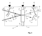
- Fig. 3:
- eine schematische Darstellung eines Strahlteilermoduls gemäß der gegenwärtigen Erfindung.
- 1
- Pulslaser
- 2
- Laserstrahl
- 3
- Einkoppeloptik
- 4
- optisches Bauelement
- 5
- erste Optik
- 6
- breitbandiges Beleuchtungslicht
- 7
- wellenlängen- und/oder intensitätsselektierendes Mittel
- 8
- Beleuchtungslicht
- 9
- zweite Optik
- 10
- Beleuchtungspinhole
- 11
- Strahlteiler
- 12
- Scanspiegel
- 13
- Objektiv
- 14
- Probe
- 15
- Detektionslicht
- 16
- Detektionspinhole
- 17
- Detektor
- 18
- Referenzdetektor
- 20
- Regelungselektronik
- 29
- Senkrechte auf den Strahlteiler
- 30
- Substrat
- 31
- Beschichtung
- 32
- Blende
- 33
- Blende
- 35
- Reflex
- 36
- Reflex
- 38
- dritter Strahlteiler
- 39
- Referenzstrahl
- 40
- optisches Bauelement
- 41
- Gehäuse
- 42
- Halterung
- 44
- Halterung
- 46
- Justagemittel
- 48
- erste Öffnung
- 49
- zweite Öffnung
- 50
- dritte Öffnung
- α/2
- Winkel
Claims (16)
- Scanmikroskop mit einem Objektiv (13), durch das eine Probe (14) beleuchtbar und detektierbar ist, wobei das Objektiv (13) sowohl in einem Beleuchtungs- als auch einem Detektionsstrahlengang (8, 15) angeordnet ist, und dass ein Beleuchtungs- und Detektionspinhole (10, 16) jeweils im Beleuchtungs- bzw. im Detektionsstrahlengang (8, 15) angeordnet ist, dadurch gekennzeichnet, dass im Beleuchtungsstrahlengang (8) ein optisches Bauelement (4) vorgesehen ist, das ein zumindest teilweise spektral verbreitertes Beleuchtungslicht erzeugt, und dass ein im wesentlichen polarisations- und wellenlängenunabhängiger Strahlteiler (11) im Beleuchtungs- und Detektionsstrahlengang (8, 15) ortsfest angeordnet ist.
- Scanmikroskop nach Anspruch 1, dadurch gekennzeichnet, dass eine Lichtquelle mindestens einen Laser (1) umfasst, dessen Licht in das optische Bauelement (4) einkoppelbar ist, und dass das optische Bauelement (4) aus mikrostrukturiertem Material besteht.
- Scanmikroskop nach Anspruch 2, dadurch gekennzeichnet, dass der Laser (1) ein gepulster Laser ist.
- Scanmikroskop nach Anspruch 1, dadurch gekennzeichnet, dass der polarisations- und wellenlängenunabhängige Strahlteiler (11) derart angeordnet ist, dass das Beleuchtungslicht (8) bezüglich der Senkrechten (29) des Strahlteilers (11) unter einem derartigen Winkel (α/2) auftrifft, dass Polarisationseffekte minimal sind.
- Scanmikroskop nach Anspruch 4, dadurch gekennzeichnet, dass der Winkel (α/2) bezüglich der Senkrechten (29) des Strahlteilers (11) im Bereich von 1 bis 30 Grad liegt.
- Scanmikroskop nach Anspruch 1, dadurch gekennzeichnet, dass ein Referenzdetektor (18) in einem durch den Strahlteiler (11) hindurchtretenden Licht definierten Referenzstrahl (39) angeordnet ist, der aus dem Licht des Referenzstrahls (39) eine elektronische Größe ermittelt, die an eine Regelungselektronik (20) überführbar ist.
- Scanmikroskop nach Anspruch 6, dadurch gekennzeichnet, dass die Regelungselektronik 20 mit dem wellenlängen- und/oder intensitätsselektierenden Mittel 7 verbunden ist, wobei die Regelungselektronik 20 die Intensität des Beleuchtungslichts 8 derart regelt, dass an der Probe 14 immer eine konstante Lichtleistung herrscht.
- Scanmikroskop nach einem der Ansprüche 1 bis 7, dadurch gekennzeichnet, dass der polarisations- und wellenlängenunabhängige Strahlteiler (11), das Beleuchtungspinhole (10), das Detektionspinhole (16) und der Referenzdetektor (18) in einem Gehäuse (41) angeordnet sind.
- Optisches Bauelement (40) zum Einsetzen in einen Beleuchtung- und Detektionsstrahlengang (8, 15) eines Scanmikroskops, dadurch gekennzeichnet, dass das optische Bauelement (40) einen polarisations- und wellenlängenunabhängigen Strahlteiler (11), ein Beleuchtungspinhole (10), ein Detektionspinhole (16) und einen Referenzdetektor (18) umfasst.
- Optisches Bauelement (40) nach Anspruch 9, dadurch gekennzeichnet, dass ein Gehäuse (41) vorgesehen ist, das den Strahlteiler (11), das Beleuchtungspinhole(10), das Detektionspinhole (16) und den Referenzdetektor (18) beinhaltet, und derart im Beleuchtungs- und Detektionsstrahlengang (8, 15) des Scanmikroskops angeordnet ist, dass das Beleuchtungslicht bezüglich der Senkrechten (29) des Strahlteilers (11) unter einem derartigen Winkel α/2 auftrifft, dass Polarisationseffekte minimal sind.
- Optisches Bauelement (40) nach Anspruch 9, dadurch gekennzeichnet, dass dem Strahlteiler (11), dem Beleuchtungspinhole (10) und dem Detektionspinhole (16) jeweils mindestens ein Justagemittel (46) zugeordnet ist.
- Optisches Bauelement (40) nach Anspruch 9, dadurch gekennzeichnet, dass das Scanmikroskop eine Lichtquelle umfasst, die aus mindestens einem Laser (1) und einem mikrostrukturiertem Material (4) besteht, in das das Licht des Lasers (1) einkoppelbar ist.
- Optisches Bauelement (40) nach Anspruch 9, dadurch gekennzeichnet, dass der Strahlteiler (11) aus einem Substrat (30) und einer reflektierenden Beschichtung (31) besteht.
- Optisches Bauelement (40) nach Anspruch 9, dadurch gekennzeichnet, dass der Referenzdetektor (18) in einem durch den Strahlteiler (11) hindurchtretendes Licht definierten Referenzstrahl (39) angeordnet ist, der aus dem Licht des Referenzstrahls (39) eine elektronische Größe ermittelt, die an eine Regelungselektronik (20) überführbar ist.
- Optisches Bauelement (40) nach Anspruch 14, dadurch gekennzeichnet, dass die Regelungselektronik (20) mit dem wellenlängen- und/oder intensitätsselektierendes Mittel 7 verbunden ist, wobei die Regelungselektronik 20 die Intensität des Beleuchtungslichts 8 derart regelt, dass an der Probe 14 immer eine konstante Lichtleistung herrscht.
- Optisches Bauelement (40) nach Anspruch 9, dadurch gekennzeichnet, dass bei dem in den Beleuchtungs- und Detektionsstrahlengang (8, 15) eingebrachten Gehäuse (41) der Strahlteiler (11) ortsfest bezüglich des Beleuchtungs- und Detektionsstrahlenganges (8, 15) angeordnet ist.
Applications Claiming Priority (4)
| Application Number | Priority Date | Filing Date | Title |
|---|---|---|---|
| DE10030013 | 2000-06-17 | ||
| DE10030013 | 2000-06-17 | ||
| DE10115577 | 2001-03-29 | ||
| DE10115577A DE10115577A1 (de) | 2000-06-17 | 2001-03-29 | Scanmikroskop mit mehrbandiger Beleuchtung und optisches Bauteil für ein Scanmikroskop mit mehrbandiger Beleuchtung |
Publications (2)
| Publication Number | Publication Date |
|---|---|
| EP1164402A1 true EP1164402A1 (de) | 2001-12-19 |
| EP1164402B1 EP1164402B1 (de) | 2010-04-28 |
Family
ID=26006135
Family Applications (1)
| Application Number | Title | Priority Date | Filing Date |
|---|---|---|---|
| EP01112882A Expired - Lifetime EP1164402B1 (de) | 2000-06-17 | 2001-06-01 | Scanmikroskop mit mehrbandiger Beleuchtung und optisches Bauelement für ein Scanmikroskop mit mehrbandiger Beleuchtung |
Country Status (3)
| Country | Link |
|---|---|
| US (1) | US6654166B2 (de) |
| EP (1) | EP1164402B1 (de) |
| JP (1) | JP4898023B2 (de) |
Families Citing this family (21)
| Publication number | Priority date | Publication date | Assignee | Title |
|---|---|---|---|---|
| US6898367B2 (en) * | 2000-06-17 | 2005-05-24 | Leica Microsystems Heidelberg Gmbh | Method and instrument for microscopy |
| DE10115487A1 (de) * | 2000-06-17 | 2001-12-20 | Leica Microsystems | Anordnung zum Untersuchen mikroskopischer Präparate mit einem Scanmikroskop |
| DE20122783U1 (de) * | 2000-06-17 | 2007-11-15 | Leica Microsystems Cms Gmbh | Anordnung zum Untersuchen mikroskopischer Präparate mit einem Scanmikroskop und Beleuchtungseinrichtung für ein Scanmikroskop |
| JP4685229B2 (ja) * | 2000-10-31 | 2011-05-18 | オリンパス株式会社 | レーザ顕微鏡 |
| DE10137158B4 (de) * | 2001-07-30 | 2005-08-04 | Leica Microsystems Heidelberg Gmbh | Verfahren zur Scanmikroskopie und Scanmikroskop |
| DE20205081U1 (de) * | 2002-03-30 | 2002-06-06 | Leica Microsystems Heidelberg Gmbh, 68165 Mannheim | Mikroskop mit einer Vorrichtung zur Ermittlung der Lichtleistung eines Beleuchtungslichtstrahls |
| DE10227111B4 (de) * | 2002-06-17 | 2007-09-27 | Leica Microsystems Cms Gmbh | Spektralmikroskop und Verfahren zur Datenaufnahme mit einem Spektralmikroskop |
| DE10332064A1 (de) * | 2003-07-11 | 2005-01-27 | Carl Zeiss Jena Gmbh | Anordnung zur Erfassung der Beleuchtungsstrahlung ineinem Laser-Scanning-Mikroskop |
| DE10331906B4 (de) * | 2003-07-15 | 2005-06-16 | Leica Microsystems Heidelberg Gmbh | Lichtquelle mit einem Mikrostruktuierten optischen Element und Mikroskop mit Lichtquelle |
| DE10340964A1 (de) * | 2003-09-05 | 2005-03-31 | Leica Microsystems Heidelberg Gmbh | Lichtquelle mit einem mikrostrukturierten optischen Element |
| JP2005140981A (ja) * | 2003-11-06 | 2005-06-02 | Nikon Corp | 顕微鏡装置 |
| WO2005088382A1 (en) * | 2004-03-16 | 2005-09-22 | Sign-Tronic Ag | Method for establishing a light beam with substantially constant luminous intensity |
| DE102004026931B3 (de) * | 2004-06-01 | 2005-12-22 | Schott Ag | Breitbandige Lichtquelle, welche ein breitbandiges Spektrum aufweist, und ein Kurzkohärenz-Meßgerät, das eine derartige Lichtquelle aufweist |
| US7133590B2 (en) * | 2005-03-17 | 2006-11-07 | The United States Of America As Represented By The Secretary Of The Navy | IR supercontinuum source |
| DE102005059338A1 (de) * | 2005-12-08 | 2007-06-14 | Carl Zeiss Jena Gmbh | Verfahren und Anordnung zur Untersuchung von Proben |
| JP4981460B2 (ja) * | 2007-01-16 | 2012-07-18 | オリンパス株式会社 | レーザ顕微鏡 |
| US7936503B2 (en) * | 2007-02-19 | 2011-05-03 | Olympus Corporation | Laser scanning microscope |
| US8421007B2 (en) * | 2011-05-18 | 2013-04-16 | Tohoku University | X-ray detection system |
| EP3538941B1 (de) | 2016-11-10 | 2025-04-23 | The Trustees of Columbia University in the City of New York | Schnelles hochauflösendes bildgebungsverfahren für grosse proben |
| JP6876574B2 (ja) * | 2017-08-14 | 2021-05-26 | 日本電子株式会社 | X線分析装置およびスペクトル生成方法 |
| US11885743B2 (en) * | 2020-07-22 | 2024-01-30 | Agar Corporation, Inc. | Fluorescence and scatter and absorption spectroscopic apparatus with a sapphire tube and method for analyzing inline low level hydrocarbon in a flow medium |
Citations (3)
| Publication number | Priority date | Publication date | Assignee | Title |
|---|---|---|---|---|
| US5161053A (en) * | 1988-08-01 | 1992-11-03 | Commonwealth Scientific & Industrial Research | Confocal microscope |
| DE19622359A1 (de) * | 1996-06-04 | 1997-12-11 | Zeiss Carl Jena Gmbh | Vorrichtung zur Einkopplung der Strahlung von Kurzpulslasern in einem mikroskopischen Strahlengang |
| DE19702753A1 (de) * | 1997-01-27 | 1998-07-30 | Zeiss Carl Jena Gmbh | Laser-Scanning-Mikroskop |
Family Cites Families (9)
| Publication number | Priority date | Publication date | Assignee | Title |
|---|---|---|---|---|
| US5127730A (en) * | 1990-08-10 | 1992-07-07 | Regents Of The University Of Minnesota | Multi-color laser scanning confocal imaging system |
| JPH05332733A (ja) * | 1992-05-27 | 1993-12-14 | Hitachi Ltd | 検出光学系並びに立体形状検出方法 |
| US5537247A (en) * | 1994-03-15 | 1996-07-16 | Technical Instrument Company | Single aperture confocal imaging system |
| US5903688A (en) * | 1994-08-25 | 1999-05-11 | Leica Lasertechnik Gmbh | Device for feeding a UV laser into a confocal laser scanning microscope |
| US5861984A (en) * | 1995-03-31 | 1999-01-19 | Carl Zeiss Jena Gmbh | Confocal scanning microscope and beamsplitter therefor |
| KR100209608B1 (ko) * | 1995-09-15 | 1999-07-15 | 구자홍 | 광 출력검지 장치 |
| US6108127A (en) * | 1997-05-15 | 2000-08-22 | 3M Innovative Properties Company | High resolution confocal microscope |
| DE19829954A1 (de) * | 1998-07-04 | 2000-01-05 | Zeiss Carl Jena Gmbh | Strahlteiler in einem Laser-Scanning-Mikroskop |
| DE19842153C2 (de) * | 1998-09-15 | 2003-07-31 | Leica Microsystems | Fluoreszenzmikroskop |
-
2001
- 2001-06-01 EP EP01112882A patent/EP1164402B1/de not_active Expired - Lifetime
- 2001-06-15 US US09/881,047 patent/US6654166B2/en not_active Expired - Lifetime
- 2001-06-18 JP JP2001183689A patent/JP4898023B2/ja not_active Expired - Lifetime
Patent Citations (3)
| Publication number | Priority date | Publication date | Assignee | Title |
|---|---|---|---|---|
| US5161053A (en) * | 1988-08-01 | 1992-11-03 | Commonwealth Scientific & Industrial Research | Confocal microscope |
| DE19622359A1 (de) * | 1996-06-04 | 1997-12-11 | Zeiss Carl Jena Gmbh | Vorrichtung zur Einkopplung der Strahlung von Kurzpulslasern in einem mikroskopischen Strahlengang |
| DE19702753A1 (de) * | 1997-01-27 | 1998-07-30 | Zeiss Carl Jena Gmbh | Laser-Scanning-Mikroskop |
Non-Patent Citations (1)
| Title |
|---|
| RANKA J K ET AL: "VISIBLE CONTINUUM GENERATION IN AIR-SILICA MICROSTRUCTURE OPTICAL FIBERS WITH ANOMALOUS DISPERSION AT 800 NM", OPTICS LETTERS, OPTICAL SOCIETY OF AMERICA, WASHINGTON, US, vol. 25, no. 1, 1 January 2000 (2000-01-01), pages 25 - 27, XP000928530, ISSN: 0146-9592 * |
Also Published As
| Publication number | Publication date |
|---|---|
| JP2002055283A (ja) | 2002-02-20 |
| JP4898023B2 (ja) | 2012-03-14 |
| US20020050564A1 (en) | 2002-05-02 |
| US6654166B2 (en) | 2003-11-25 |
| EP1164402B1 (de) | 2010-04-28 |
Similar Documents
| Publication | Publication Date | Title |
|---|---|---|
| EP1164402B1 (de) | Scanmikroskop mit mehrbandiger Beleuchtung und optisches Bauelement für ein Scanmikroskop mit mehrbandiger Beleuchtung | |
| DE10115577A1 (de) | Scanmikroskop mit mehrbandiger Beleuchtung und optisches Bauteil für ein Scanmikroskop mit mehrbandiger Beleuchtung | |
| EP1184701B1 (de) | Beleuchtungseinrichtung | |
| DE10243449B4 (de) | CARS-Mikroskop und Verfahren zur CARS-Mikroskopie | |
| EP0941470B1 (de) | Fluoreszenzkorrelationsspektroskopiemodul für ein mikroskop | |
| EP1164406A2 (de) | Verfahren und Vorrichtung zur Beleuchtung eines Objekts | |
| DE69334168T2 (de) | Spektrometer für linsenmesser | |
| DE4200869C2 (de) | Infrarot Mikroskop-Spektrometer | |
| EP1186854A2 (de) | Beleuchtungs- und Abbildungseinrichtung für mehrere Spektralbereiche und Koordinatenmessmaschine mit einer Beleuchtungs- und Abbildungseinrichtung für mehrere Spektralbereiche | |
| DE102022132453A1 (de) | Vorrichtung und Verfahren zum Bestimmen einer Abbildungsqualität zumindest einer Abbildung für einen Prüfling | |
| EP1505424A1 (de) | Rastermikroskop mit optischer Einkoppelvorrichtung für externes Licht | |
| EP1651992A1 (de) | Rastermikroskop | |
| EP1089061A2 (de) | Laserscanmikroskop und Verfahren zur Referenzkorrektur bei einem Laserscanmikroskop | |
| DE69025702T2 (de) | Mikroskopisches Spektrometer | |
| EP3614130A1 (de) | Vorrichtung zur ermittlung optischer eigenschaften von proben | |
| DE10021379A1 (de) | Optische Messanordnung insbesondere zur Schichtdickenmessung | |
| DE10324478B3 (de) | Vorrichtung zum Ermitteln der Lichtleistung eines Lichtstrahles und Scanmikroskop | |
| DE2021324C3 (de) | Photometer für Beobachtungsgeräte, insbesondere für Mikroskope | |
| DE20122790U1 (de) | Scanmikroskop mit mehrbandiger Beleuchtung und optisches Bauteil für ein Scanmikroskop mit mehrbandiger Beleuchtung | |
| DE102004035340B4 (de) | Rastermikroskop mit einer Strahlablenkeinrichtung | |
| DE3730548A1 (de) | Messgeraet zum vermessen und justieren von laserentfernungsmessern | |
| DE2655859C2 (de) | Ophthalmologisches Gerät zur Untersuchung und zum Fotografieren des Augenhintergrundes | |
| DE10031458A1 (de) | Scan-Mikroskop mit einem Zirkulator | |
| EP1353210B1 (de) | Mikroskop mit einer Vorrichtung zur Ermittlung der Lichtleistung eines Beleuchtungslichtstrahls | |
| DE10102033B4 (de) | Vorrichtung und Scanmikroskop zur gleichzeitigen Detektion mehrerer Spektralbereiche eines Lichtstrahls |
Legal Events
| Date | Code | Title | Description |
|---|---|---|---|
| PUAI | Public reference made under article 153(3) epc to a published international application that has entered the european phase |
Free format text: ORIGINAL CODE: 0009012 |
|
| AK | Designated contracting states |
Kind code of ref document: A1 Designated state(s): DE FR GB Kind code of ref document: A1 Designated state(s): AT BE CH CY DE DK ES FI FR GB GR IE IT LI LU MC NL PT SE TR |
|
| AX | Request for extension of the european patent |
Free format text: AL;LT;LV;MK;RO;SI |
|
| 17P | Request for examination filed |
Effective date: 20020618 |
|
| AKX | Designation fees paid |
Free format text: DE FR GB |
|
| RAP1 | Party data changed (applicant data changed or rights of an application transferred) |
Owner name: LEICA MICROSYSTEMS CMS GMBH |
|
| GRAP | Despatch of communication of intention to grant a patent |
Free format text: ORIGINAL CODE: EPIDOSNIGR1 |
|
| GRAS | Grant fee paid |
Free format text: ORIGINAL CODE: EPIDOSNIGR3 |
|
| GRAA | (expected) grant |
Free format text: ORIGINAL CODE: 0009210 |
|
| AK | Designated contracting states |
Kind code of ref document: B1 Designated state(s): DE FR GB |
|
| REG | Reference to a national code |
Ref country code: GB Ref legal event code: FG4D Free format text: NOT ENGLISH |
|
| REF | Corresponds to: |
Ref document number: 50115456 Country of ref document: DE Date of ref document: 20100610 Kind code of ref document: P |
|
| PLBE | No opposition filed within time limit |
Free format text: ORIGINAL CODE: 0009261 |
|
| STAA | Information on the status of an ep patent application or granted ep patent |
Free format text: STATUS: NO OPPOSITION FILED WITHIN TIME LIMIT |
|
| 26N | No opposition filed |
Effective date: 20110131 |
|
| REG | Reference to a national code |
Ref country code: DE Ref legal event code: R082 Ref document number: 50115456 Country of ref document: DE Representative=s name: SCHAUMBURG & PARTNER PATENTANWAELTE GBR, DE Ref country code: DE Ref legal event code: R082 Ref document number: 50115456 Country of ref document: DE Representative=s name: SCHAUMBURG UND PARTNER PATENTANWAELTE MBB, DE |
|
| REG | Reference to a national code |
Ref country code: FR Ref legal event code: PLFP Year of fee payment: 16 |
|
| REG | Reference to a national code |
Ref country code: FR Ref legal event code: PLFP Year of fee payment: 17 |
|
| REG | Reference to a national code |
Ref country code: FR Ref legal event code: PLFP Year of fee payment: 18 |
|
| PGFP | Annual fee paid to national office [announced via postgrant information from national office to epo] |
Ref country code: FR Payment date: 20200626 Year of fee payment: 20 |
|
| PGFP | Annual fee paid to national office [announced via postgrant information from national office to epo] |
Ref country code: GB Payment date: 20200630 Year of fee payment: 20 |
|
| PGFP | Annual fee paid to national office [announced via postgrant information from national office to epo] |
Ref country code: DE Payment date: 20200827 Year of fee payment: 20 |
|
| REG | Reference to a national code |
Ref country code: DE Ref legal event code: R071 Ref document number: 50115456 Country of ref document: DE |
|
| REG | Reference to a national code |
Ref country code: GB Ref legal event code: PE20 Expiry date: 20210531 |
|
| PG25 | Lapsed in a contracting state [announced via postgrant information from national office to epo] |
Ref country code: GB Free format text: LAPSE BECAUSE OF EXPIRATION OF PROTECTION Effective date: 20210531 |