EP1160972A2 - Electronic parts - Google Patents

Electronic parts Download PDF

Info

Publication number
EP1160972A2
EP1160972A2 EP00311741A EP00311741A EP1160972A2 EP 1160972 A2 EP1160972 A2 EP 1160972A2 EP 00311741 A EP00311741 A EP 00311741A EP 00311741 A EP00311741 A EP 00311741A EP 1160972 A2 EP1160972 A2 EP 1160972A2
Authority
EP
European Patent Office
Prior art keywords
dielectric
composite
dielectric constant
constituent layers
layers
Prior art date
Legal status (The legal status is an assumption and is not a legal conclusion. Google has not performed a legal analysis and makes no representation as to the accuracy of the status listed.)
Withdrawn
Application number
EP00311741A
Other languages
German (de)
French (fr)
Other versions
EP1160972A3 (en
Inventor
Minoru Takaya
Toshikazu Endo
Current Assignee (The listed assignees may be inaccurate. Google has not performed a legal analysis and makes no representation or warranty as to the accuracy of the list.)
TDK Corp
Original Assignee
TDK Corp
Priority date (The priority date is an assumption and is not a legal conclusion. Google has not performed a legal analysis and makes no representation as to the accuracy of the date listed.)
Filing date
Publication date
Application filed by TDK Corp filed Critical TDK Corp
Publication of EP1160972A2 publication Critical patent/EP1160972A2/en
Publication of EP1160972A3 publication Critical patent/EP1160972A3/en
Withdrawn legal-status Critical Current

Links

Images

Classifications

    • HELECTRICITY
    • H03ELECTRONIC CIRCUITRY
    • H03HIMPEDANCE NETWORKS, e.g. RESONANT CIRCUITS; RESONATORS
    • H03H7/00Multiple-port networks comprising only passive electrical elements as network components
    • H03H7/01Frequency selective two-port networks
    • H03H7/0115Frequency selective two-port networks comprising only inductors and capacitors
    • HELECTRICITY
    • H03ELECTRONIC CIRCUITRY
    • H03HIMPEDANCE NETWORKS, e.g. RESONANT CIRCUITS; RESONATORS
    • H03H7/00Multiple-port networks comprising only passive electrical elements as network components
    • H03H7/01Frequency selective two-port networks
    • H03H7/09Filters comprising mutual inductance
    • HELECTRICITY
    • H03ELECTRONIC CIRCUITRY
    • H03HIMPEDANCE NETWORKS, e.g. RESONANT CIRCUITS; RESONATORS
    • H03H1/00Constructional details of impedance networks whose electrical mode of operation is not specified or applicable to more than one type of network
    • H03H2001/0021Constructional details
    • H03H2001/0085Multilayer, e.g. LTCC, HTCC, green sheets
    • YGENERAL TAGGING OF NEW TECHNOLOGICAL DEVELOPMENTS; GENERAL TAGGING OF CROSS-SECTIONAL TECHNOLOGIES SPANNING OVER SEVERAL SECTIONS OF THE IPC; TECHNICAL SUBJECTS COVERED BY FORMER USPC CROSS-REFERENCE ART COLLECTIONS [XRACs] AND DIGESTS
    • Y10TECHNICAL SUBJECTS COVERED BY FORMER USPC
    • Y10TTECHNICAL SUBJECTS COVERED BY FORMER US CLASSIFICATION
    • Y10T428/00Stock material or miscellaneous articles
    • Y10T428/24Structurally defined web or sheet [e.g., overall dimension, etc.]
    • Y10T428/24802Discontinuous or differential coating, impregnation or bond [e.g., artwork, printing, retouched photograph, etc.]
    • Y10T428/24917Discontinuous or differential coating, impregnation or bond [e.g., artwork, printing, retouched photograph, etc.] including metal layer
    • YGENERAL TAGGING OF NEW TECHNOLOGICAL DEVELOPMENTS; GENERAL TAGGING OF CROSS-SECTIONAL TECHNOLOGIES SPANNING OVER SEVERAL SECTIONS OF THE IPC; TECHNICAL SUBJECTS COVERED BY FORMER USPC CROSS-REFERENCE ART COLLECTIONS [XRACs] AND DIGESTS
    • Y10TECHNICAL SUBJECTS COVERED BY FORMER USPC
    • Y10TTECHNICAL SUBJECTS COVERED BY FORMER US CLASSIFICATION
    • Y10T428/00Stock material or miscellaneous articles
    • Y10T428/24Structurally defined web or sheet [e.g., overall dimension, etc.]
    • Y10T428/24942Structurally defined web or sheet [e.g., overall dimension, etc.] including components having same physical characteristic in differing degree
    • YGENERAL TAGGING OF NEW TECHNOLOGICAL DEVELOPMENTS; GENERAL TAGGING OF CROSS-SECTIONAL TECHNOLOGIES SPANNING OVER SEVERAL SECTIONS OF THE IPC; TECHNICAL SUBJECTS COVERED BY FORMER USPC CROSS-REFERENCE ART COLLECTIONS [XRACs] AND DIGESTS
    • Y10TECHNICAL SUBJECTS COVERED BY FORMER USPC
    • Y10TTECHNICAL SUBJECTS COVERED BY FORMER US CLASSIFICATION
    • Y10T428/00Stock material or miscellaneous articles
    • Y10T428/249921Web or sheet containing structurally defined element or component
    • Y10T428/249924Noninterengaged fiber-containing paper-free web or sheet which is not of specified porosity
    • Y10T428/249928Fiber embedded in a ceramic, glass, or carbon matrix
    • YGENERAL TAGGING OF NEW TECHNOLOGICAL DEVELOPMENTS; GENERAL TAGGING OF CROSS-SECTIONAL TECHNOLOGIES SPANNING OVER SEVERAL SECTIONS OF THE IPC; TECHNICAL SUBJECTS COVERED BY FORMER USPC CROSS-REFERENCE ART COLLECTIONS [XRACs] AND DIGESTS
    • Y10TECHNICAL SUBJECTS COVERED BY FORMER USPC
    • Y10TTECHNICAL SUBJECTS COVERED BY FORMER US CLASSIFICATION
    • Y10T428/00Stock material or miscellaneous articles
    • Y10T428/249921Web or sheet containing structurally defined element or component
    • Y10T428/249924Noninterengaged fiber-containing paper-free web or sheet which is not of specified porosity
    • Y10T428/24994Fiber embedded in or on the surface of a polymeric matrix
    • Y10T428/249941Fiber is on the surface of a polymeric matrix having no embedded portion
    • YGENERAL TAGGING OF NEW TECHNOLOGICAL DEVELOPMENTS; GENERAL TAGGING OF CROSS-SECTIONAL TECHNOLOGIES SPANNING OVER SEVERAL SECTIONS OF THE IPC; TECHNICAL SUBJECTS COVERED BY FORMER USPC CROSS-REFERENCE ART COLLECTIONS [XRACs] AND DIGESTS
    • Y10TECHNICAL SUBJECTS COVERED BY FORMER USPC
    • Y10TTECHNICAL SUBJECTS COVERED BY FORMER US CLASSIFICATION
    • Y10T428/00Stock material or miscellaneous articles
    • Y10T428/29Coated or structually defined flake, particle, cell, strand, strand portion, rod, filament, macroscopic fiber or mass thereof
    • Y10T428/2982Particulate matter [e.g., sphere, flake, etc.]
    • YGENERAL TAGGING OF NEW TECHNOLOGICAL DEVELOPMENTS; GENERAL TAGGING OF CROSS-SECTIONAL TECHNOLOGIES SPANNING OVER SEVERAL SECTIONS OF THE IPC; TECHNICAL SUBJECTS COVERED BY FORMER USPC CROSS-REFERENCE ART COLLECTIONS [XRACs] AND DIGESTS
    • Y10TECHNICAL SUBJECTS COVERED BY FORMER USPC
    • Y10TTECHNICAL SUBJECTS COVERED BY FORMER US CLASSIFICATION
    • Y10T428/00Stock material or miscellaneous articles
    • Y10T428/29Coated or structually defined flake, particle, cell, strand, strand portion, rod, filament, macroscopic fiber or mass thereof
    • Y10T428/2982Particulate matter [e.g., sphere, flake, etc.]
    • Y10T428/2991Coated
    • YGENERAL TAGGING OF NEW TECHNOLOGICAL DEVELOPMENTS; GENERAL TAGGING OF CROSS-SECTIONAL TECHNOLOGIES SPANNING OVER SEVERAL SECTIONS OF THE IPC; TECHNICAL SUBJECTS COVERED BY FORMER USPC CROSS-REFERENCE ART COLLECTIONS [XRACs] AND DIGESTS
    • Y10TECHNICAL SUBJECTS COVERED BY FORMER USPC
    • Y10TTECHNICAL SUBJECTS COVERED BY FORMER US CLASSIFICATION
    • Y10T428/00Stock material or miscellaneous articles
    • Y10T428/29Coated or structually defined flake, particle, cell, strand, strand portion, rod, filament, macroscopic fiber or mass thereof
    • Y10T428/2982Particulate matter [e.g., sphere, flake, etc.]
    • Y10T428/2991Coated
    • Y10T428/2993Silicic or refractory material containing [e.g., tungsten oxide, glass, cement, etc.]
    • YGENERAL TAGGING OF NEW TECHNOLOGICAL DEVELOPMENTS; GENERAL TAGGING OF CROSS-SECTIONAL TECHNOLOGIES SPANNING OVER SEVERAL SECTIONS OF THE IPC; TECHNICAL SUBJECTS COVERED BY FORMER USPC CROSS-REFERENCE ART COLLECTIONS [XRACs] AND DIGESTS
    • Y10TECHNICAL SUBJECTS COVERED BY FORMER USPC
    • Y10TTECHNICAL SUBJECTS COVERED BY FORMER US CLASSIFICATION
    • Y10T428/00Stock material or miscellaneous articles
    • Y10T428/31504Composite [nonstructural laminate]
    • Y10T428/31678Of metal
    • YGENERAL TAGGING OF NEW TECHNOLOGICAL DEVELOPMENTS; GENERAL TAGGING OF CROSS-SECTIONAL TECHNOLOGIES SPANNING OVER SEVERAL SECTIONS OF THE IPC; TECHNICAL SUBJECTS COVERED BY FORMER USPC CROSS-REFERENCE ART COLLECTIONS [XRACs] AND DIGESTS
    • Y10TECHNICAL SUBJECTS COVERED BY FORMER USPC
    • Y10TTECHNICAL SUBJECTS COVERED BY FORMER US CLASSIFICATION
    • Y10T428/00Stock material or miscellaneous articles
    • Y10T428/32Composite [nonstructural laminate] of inorganic material having metal-compound-containing layer and having defined magnetic layer

Definitions

  • This invention relates to electronic parts and multilayer circuits using prepreg and substrate, and more particularly, to such electronic parts suitable for operation in a high frequency region of at least 100 MHz and for use in magnetic characteristics-utilizing applications and magnetic shields.
  • Known electronic parts or multilayer substrates for high frequency operation include sintered ferrite and sintered ceramics which are laminated and molded into substrate form. Laminating such materials into multilayer substrates has been practiced in the art because of the_ advantage of potential miniaturization.
  • sintered ferrite and sintered ceramics give rise to several problems. A number of steps are involved in firing and thick film printing. Sintered materials suffer from inherent defects including cracks and warp caused by firing. Cracks are also induced by the differential thermal expansion between sintered material and printed circuit board. It is thus increasingly required to replace the sintered materials by resinous materials.
  • JP-A 8-69712 and JP-A 11-192620 mix resinous materials with ceramic powder into composite materials. These composite materials, however, have unsatisfactory high-frequency characteristics and magnetic characteristics.
  • JP-B 6-14600 discloses the sheeting technique of forming plural materials into layers, followed by lamination. This method involves a number of steps.
  • the operating frequency of the multilayer part referred to in this patent is several megahertz at maximum. No study is made on the performance of the multilayer part in the high-frequency region of at least 100 MHz.
  • An object of the invention is to provide a multilayer electronic part having the advantages of small size, excellent performance and improved overall electrical characteristics, using plural layers selected from among composite resin substrates having a sufficiently high or low dielectric constant, composite resin substrates having a sufficiently high dielectric constant, and composite resin substrate layers having a sufficiently high Q value.
  • a multilayer electronic part comprising constituent layers of at least two types formed of hybrid or composite materials and a conductor layer formed on at least one composite material layer, the conductor layer constructing a predetermined electric circuit.
  • the multilayer electronic part is typically used in a frequency band of at least 100 MHz.
  • the constituent layers include a layer containing at least reinforcing fibers.
  • the constituent layers include at least one layer containing at least one flame retardant.
  • the constituent layers include at least one first composite dielectric layer in which a dielectric powder having a dielectric constant (or relative permittivity) of 5 to 10,000 and a dielectric dissipation factor of 0.00002 to 0.01 is dispersed in an amount of 10 to 65% by volume such that the first composite dielectric layer has a dielectric constant of 5 to 20 and a dielectric dissipation factor of 0.0025 to 0.0075.
  • a dielectric powder having a dielectric constant (or relative permittivity) of 5 to 10,000 and a dielectric dissipation factor of 0.00002 to 0.01 is dispersed in an amount of 10 to 65% by volume such that the first composite dielectric layer has a dielectric constant of 5 to 20 and a dielectric dissipation factor of 0.0025 to 0.0075.
  • the constituent layers include at least one second composite dielectric layer in which a dielectric powder having a dielectric constant of 20 to 20,000 and a dielectric dissipation factor of 0.01 to 0.0001 is dispersed in an amount of 10 to 65% by volume such that the second composite dielectric layer has a dielectric constant of 10 to 40 and a dielectric dissipation factor of 0.0075 to 0.025.
  • the constituent layers include at least one composite magnetic layer in which a magnetic powder is dispersed in an amount of 10 to 65% by volume such that the composite magnetic layer has a magnetic permeability of 3 to 20.
  • multilayer substrates are constructed using a composite material of at least a resin and a magnetic powder and a composite material of at least a resin and a dielectric powder.
  • the multilayer electronic part of the invention includes at least two different constituent layers formed of hybrid or composite materials and a conductor layer formed on at least one composite material layer.
  • a predetermined electric circuit is constructed by the conductor layer.
  • This construction enables to adjust a dielectric constant ⁇ and to provide a lower dielectric constant so that the part is suited for use in the high-frequency region of at least 100 MHz, and especially 100 MHz to 10 GHz.
  • the composite magnetic material layers are suitable for use in magnetic characteristic-utilizing applications and as magnetic shields.
  • the composite dielectric material layers can provide a relatively high Q and ⁇ value in the high-frequency band, and yields a composite dielectric material substrate suited for use in the application where such characteristics are required, for example, such electronic parts as strip lines, impedance matching circuits, delay circuits, and antennas. High strength is another advantage.
  • the invention enables bonding with copper foil without a need for adhesive. patterning, and lamination. Such patterning and lamination can be conducted through the same steps as conventional substrate manufacturing steps, contributing to a cost reduction and efficient manufacture. Electronic parts using the thus fabricated substrates have a high strength and improved high-frequency characteristics.
  • the resin used in the multilayer electronic part is not critical. A proper choice may be made among resin materials having good moldability, processability, adhesion during stacking, and electrical characteristics. Specifically, thermosetting resins and thermoplastic resins are preferred.
  • thermosetting resins which can be used herein include epoxy resins, phenolic resins, unsaturated polyester resins, vinyl ester resins, polyimide resins, polyphenylene ether (or oxide) resins, bismaleimide triazine (or cyanate) resins, fumarate resins, and polybutadiene resins.
  • the thermoplastic resins which can be used herein include aromatic polyester resins, polyphenylene sulfide resins, polyethylene terephthalate resins, polybutylene terephthalate resins, polyethylene sulfide resins, polyether ether ketone resins, polytetrafluoroethylene resins, and graft resins.
  • phenolic resins, epoxy resins, low dielectric constant epoxy resins, polybutadiene resins, and BT resins are preferred as the base resin.
  • These resins may be used alone or in admixture of two or more. Mixtures may have any desired mixing ratio of two or more resin components.
  • the multilayer electronic part preferably has at least one organic dielectric layer formed of the above resin and having a dielectric constant of 2.4 to 4.5 and a dielectric dissipation factor of 0.002 to 0.03.
  • Such an organic dielectric layer is especially suited in forming inductor devices such as coils since it can minimize the distributed capacitance.
  • the multilayer electronic part includes at least one first composite dielectric layer in which a dielectric powder having a dielectric constant of 5 to 10,000 and a dielectric dissipation factor of 0.01 to 0.00002 is dispersed in the resin in an amount of 10 to 65% by volume such that the first composite dielectric layer has a dielectric constant of 5 to 20 and a dielectric dissipation factor of 0.0025 to 0.0075.
  • This embodiment provides an adequate dielectric constant and a high Q value and hence, a reduced transmission loss, and is suitable in forming such electronic circuits as balun (balanced-and-unbalanced) transformers, antennas and power amplifiers.
  • the multilayer electronic part includes at least one second composite dielectric layer in which a dielectric powder having a dielectric constant of 20 to 20,000 and a dielectric dissipation factor of 0.05 to 0.0001 is dispersed in the resin in an amount of 10 to 65% by volume such that the second composite dielectric layer has a dielectric constant of 10 to 40 and a dielectric dissipation factor of 0.0075 to 0.025.
  • This embodiment provides an adequate Q value and a high dielectric constant, and is suitable in forming such electronic circuits as capacitors, patch antennas, voltage controlled oscillators (VCO) and power amplifiers.
  • the multilayer electronic part includes at least one composite magnetic layer in which a magnetic powder is dispersed in the resin in an amount of 10 to 65% by volume such that the composite magnetic layer has a magnetic permeability of 3 to 20.
  • This embodiment provides a low dielectric constant while keeping an adequate magnetic permeability, allowing the part to be used in the high-frequency region of at least 100 MHz, and especially 100 MHz to 10 GHz.
  • the above-mentioned constituent layers differ in at least one of dielectric constant, Q value, and magnetic permeability. It suffices that at least two layers which differ in at least one parameter be included.
  • one exemplary combination is at least two layers which belong to one same class, but differ in at least one parameter
  • another exemplary combination is at least two layers which belong to different classes (and naturally differ in at least one parameter), and so forth. Such layers are properly combined so as to meet the particular construction and function of an electronic part.
  • Any ceramic powder may be used herein insofar as it has a greater dielectric constant and Q value in the high-frequency region than the resin serving as a dispersing medium. It is acceptable to use two or more types of ceramic powders.
  • a ceramic powder having a dielectric constant of 10 to 20,000 and a dielectric dissipation factor of up to 0.05 is used.
  • Preferred materials include titanium-barium-neodymium base ceramics, titanium-barium-tin base ceramics, lead-calcium base ceramics, titanium dioxide base ceramics, barium titanate base ceramics, lead titanate base ceramics, strontium titanate base ceramics, calcium titanate ceramics, bismuth titanate base ceramics, magnesium titanate base ceramics, CaWO 4 base ceramics, Ba(Mg,Nb)O 3 base ceramics, Ba(Mg,Ta)O 3 base ceramics, Ba(Co,Mg,Nb)O 3 base ceramics, and Ba(Co,Mg,Ta)O 3 base ceramics.
  • the titanium dioxide base ceramics include one consisting of titanium dioxide and those ceramics containing minor amounts of additives in addition to titanium dioxide, while they should maintain the crystalline structure of titanium dioxide. The same applies to the remaining ceramics. Of the titanium dioxide base ceramics, those having the rutile structure are preferred.
  • Preferred materials include silica, alumina, zirconia, potassium titanate whiskers, calcium titanate whiskers, barium titanate whiskers, zinc oxide whiskers, chopped glass, glass beads, carbon fibers, and magnesium oxide (or talc).
  • Mixtures may have any desired mixing ratio of two or more components.
  • the ceramic powder or particles should preferably have a mean particle size of 0.1 to 100 ⁇ m, especially 0.2 to 100 ⁇ m, so that ceramic particles are effectively milled with the resin. Too small a particle size corresponds to a greater surface area, which may increase the viscosity and thixotropy upon dispersion and mixing, obstructing high loading of ceramic particles and smooth milling with the resin. Too large a particle size may interfere with uniform dispersion and mixing, and allow for substantial settlement, resulting in a heterogeneous system. Then a composition having a larger content of ceramic powder of such large particle size may fail to form a consolidated layer when molded.
  • the content of ceramic powder is generally from 10% by volume to 65% by volume provided that the total of the resin and ceramic powder is 100% by volume.
  • the content of ceramic powder is 20 to 60% by volume.
  • the ceramic powder in the first composite dielectric layer should have a high Q and a moderate dielectric constant.
  • the ceramic powder should preferably have a dielectric constant of 5 to 10,000 and a dielectric dissipation factor of 0.01 to 0.00002 at 2 GHz, and further preferably a Q value of 250 to 50,000. With this choice, a composite dielectric material having a high Q and dielectric constant is obtainable.
  • the ceramic powder is contained in the first composite dielectric layer such that the first composite dielectric layer in its entirety has a dielectric constant of 5 to 20 and a dielectric dissipation factor of 0.0025 to 0.0075.
  • the ceramic powder may also be single crystal sapphire (or similar) powder or polycrystalline alumina powder.
  • preferred types of ceramic powder are powders of dielectrics based on the following compositions. The compositions are shown together with their dielectric constant ⁇ and Q at 2 GHz.
  • Preferred among others are those dielectrics based on the compositions: TiO 2 , CaTiO 3 , SrTiO 3 , BaO-Nd 2 O 3 -TiO 2 , Bi 2 O 3 -BaO-Nd 2 O 3 -TiO 2 , BaTi 4 O 9 , Ba 2 Ti 9 O 20 , Ba 2 (Ti,Sn) 9 O 20 , MgO-TiO 2 , ZnO-TiO 2 , MgO-SiO 2 , and Al 2 O 3 .
  • the first composite dielectric layer contains the resin and ceramic powder as main components.
  • the content of ceramic powder is generally from 10% by volume to 65% by volume provided that the total of the resin and ceramic powder is 100% by volume.
  • the content of ceramic powder is 20 to 60% by volume.
  • a ceramic powder content of more than 65% by volume may fail to provide a consolidated layer and rather result in a substantial drop of Q as compared with ceramic powder-free compositions. With less than 10% by volume, ceramic powder may fail to exert the desired effect.
  • the first composite dielectric layer can have a greater dielectric constant than that of the resin alone, that is, have a dielectric constant as desired and a high Q.
  • the ceramic powder in the second composite dielectric layer should have a very high dielectric constant.
  • the ceramic powder should preferably have a dielectric constant of 20 to 20,000 and a dielectric dissipation factor of 0.05 to 0.0001. By dispersing such ceramic powder in the resin, a composite dielectric material having a higher dielectric constant is obtainable.
  • any desired ceramic powder may be used in the second composite dielectric layer as long as the second composite dielectric layer in its entirety has a dielectric constant of 10 to 40 and a dielectric dissipation factor of 0.0075 to 0.025 in the high-frequency region, especially at 2 GHz. It is acceptable to use two or more ceramic powders.
  • Preferred types of ceramic powder are powders of dielectrics based on the following compositions. The compositions are shown together with their dielectric constant ⁇ at 2 GHz. Composition ⁇ BaTiO 3 1,500 (Ba,Pb)TiO 3 6,000 Ba(Ti,Zr)O 3 9,000 (Ba,Sr)TiO 3 7,000
  • Preferred among others are those dielectrics based on the compositions: BaTiO 3 and Ba(Ti, Zr)O 3 .
  • the ceramic powder may also be a single crystal or polycrystalline powder.
  • the ceramic powder or particles should preferably have a mean particle size of 0.2 to 100 ⁇ m so that ceramic particles are effectively milled with the resin. Particles with too small a particle size may be difficult to mill with the resin. Too large a particle size may interfere with uniform dispersion and mixing. Then a composition having a larger content of ceramic powder of such large particle size may fail to form a consolidated layer when molded.
  • the second composite dielectric layer contains the resin and ceramic powder as main components.
  • the content of ceramic powder is generally from 10% by volume to 65% by volume provided that the total of the resin and ceramic powder is 100% by volume.
  • the content of ceramic powder is 20 to 60% by volume.
  • the layers contain a magnetic powder, typically ferrite or ferromagnetic metal.
  • a magnetic powder typically ferrite or ferromagnetic metal.
  • the ferrite are Mn-Mg-Zn, Ni-Zn, Mn-Zn base systems, with the Mn-Mg-Zn and Ni-Zn base systems being preferred.
  • Exemplary ferromagnetic metals are iron carbonyl, iron-silicon base alloys, iron-aluminum-silicon base alloys (trade name: Sendust), iron-nickel base alloys (trade name: Permalloy), and amorphous alloys including iron and cobalt base alloys.
  • Means for dividing these materials into particles may be well-known techniques such as grinding and granulation.
  • the magnetic powder or particles should preferably have a particle size of 0.01 to 100 ⁇ m, especially 0.01 to 50 ⁇ m, and a mean particle size of 1 to 50 ⁇ m. Magnetic particles with a size in this range are effectively dispersed, achieving a better effect. Too small a particle size corresponds to a greater specific surface area, which may obstruct high loading of magnetic particles. Too large a particle size may allow particles to settle in forming a paste, failing to achieve uniform dispersion. When a composition of such large particles is formed into thin-wall substrates or prepregs, few may have a smooth surface. Since it is practically difficult to divide the material into particles of an extremely small size, the lower limit of particle size is about 0.01 ⁇ m.
  • the magnetic powder has a uniform distribution of particle size. If desired, a fraction of particles having a uniform particle size is collected by sieving.
  • the magnetic particles may have any desired shape including spherical, flat and elliptic shapes. A choice may be made depending on a particular application. If desired, magnetic particles may be subjected on their surface to such treatment as oxidation, coupling or coating of organic insulating material.
  • magnétique powders which differ in type or particle size distribution.
  • Such different magnetic powders may be mixed in any desired ratio.
  • the type, particle size and mixing ratio of magnetic powder may be determined depending on a particular application.
  • the magnetic powder preferably has a magnetic permeability ⁇ of 10 to 1,000,000. It is preferred that the magnetic powder in bulk form have greater insulation because substrates formed therefrom are improved in insulation.
  • the resin and magnetic powder are preferably mixed in such a ratio that the composite magnetic layer in its entirety has a magnetic permeability of 3 to 20.
  • the content of magnetic powder is 10 to 65% by volume, especially 20 to 60% by volume, based on the total of resin and magnetic powder.
  • a magnetic powder content within this range ensures that the composite magnetic layer in its entirety has a magnetic permeability of 3 to 20, achieving the desired effect. Too large a magnetic powder content may make it difficult to form a slurry for coating and hence, to form a substrate or prepreg. Too small a magnetic powder content may fail to provide the desired magnetic permeability, detracting from magnetic characteristics.
  • the flame retardant used herein may be selected from a variety of flame retardants which are conventionally used for rendering substrates flame retardant.
  • Exemplary flame retardants include halides such as halogenated phosphates and brominated epoxy resins, organic compounds such as phosphate amides, and inorganic substances such as antimony trioxide and aluminum hydride.
  • the glass cloth preferably has a thickness of up to 100 ⁇ m, more preferably 20 to 60 ⁇ m, and a weight of up to 120 g/m 2 , especially 20 to 70 g/m 2 .
  • the resin and glass cloth are mixed in a weight ratio of from 4/1 to 1/1.
  • a mixing ratio within this range ensures to exert the desired effect.
  • the resulting composite material may lose adhesion to copper foil and form a less flat substrate.
  • the choice of glass cloth which can be used may become difficult and it may become difficult to ensure the strength of a thin-wall substrate.
  • the metal foil used herein as the conductor layer may be selected from metals having good electrical conductivity such as gold. silver, copper and aluminum. Of these, copper is especially preferred.
  • the metal foil may be formed by well-known methods such as electrolysis and rolling. Electrolytic foil is preferably used where it is desired to provide a foil peel strength. Rolled foil which is least affected by the skin effect due to surface irregularities is preferably used where high-frequency characteristics are important.
  • the metal foil preferably has a gage of about 8 to 70 ⁇ m, especially about 12 to 35 ⁇ m.
  • Prepreg sheets from which electronic parts are fabricated are prepared by mixing the ceramic powder, magnetic powder and optional flame retardant with the resin in a predetermined blend ratio, and milling the ingredients in a solvent into a slurry, followed by coating and drying to B stage.
  • the solvent used herein for adjusting the viscosity of the paste for ease of coating is preferably a volatile solvent, especially a polar neutral solvent. Milling may be effected by well-known techniques such as ball milling and agitation.
  • a prepreg sheet can be fabricated by coating the paste onto a metal foil or impregnating glass cloth with the paste.
  • Drying of the prepreg sheet to B stage may be appropriately adjusted depending on the contents of ceramic powder, magnetic powder, and optional flame retardant.
  • the B stage prepreg sheet preferably has a thickness of about 50 to 300 ⁇ m and can be adjusted to an optimum thickness depending on the intended application and required characteristics (including pattern width. precision and dc resistance).
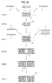
  • the prepreg sheet can be fabricated by the method shown in FIGS. 63A to 63D or 64A to 64D.
  • the method of FIGS. 63A to 63D are rather suitable for mass manufacture whereas the method of FIGS. 64A to 64D is easy to control the film thickness and relatively easy to adjust the Characteristics.
  • a glass cloth 101a wound in roll form is unraveled from the roll 101a and carried into a coating tank 110 via a guide roller 111.
  • the coating tank 110 contains a slurry having the resin, ceramic powder, magnetic powder and optional flame retardant dispersed in a solvent. As the glass cloth passes through the coating tank 110, it is immersed in the slurry so that it is coated with the slurry while interstices are filled therewith.
  • the glass cloth is carried into a drying furnace 120 via guide rollers 112a and 112b.
  • the resin-impregnated glass cloth is dried at a predetermined temperature for a predetermined time whereby it is B-staged.
  • the glass cloth is wound on a take-up roll 130.
  • the glass cloth is then cut into sections of a predetermined size. As shown in FIG. 63B, there is obtained a prepreg sheet having the glass cloth 101 sandwiched between the layers 102 of the resin containing the ceramic powder, magnetic powder and optional flame retardant.
  • metal foils 103 such as copper foils are placed on opposite surface of the prepreg sheet.
  • Laminating press yields a double side metal foil-clad substrate as shown in FIG. 63D.
  • Laminating press may be effected in plural stages under different conditions. Where the metal foils are not attached, the sandwich structure of prepreg sheet may be lamination pressed without placing metal foils thereon.
  • FIGS. 64A to 64D the method of FIGS. 64A to 64D is described.
  • a slurry 102a having the resin, ceramic powder, magnetic powder and optional flame retardant dispersed in a solvent is coated onto a metal foil such as a copper foil by means of a doctor blade 150 which can maintain a constant clearance.
  • the coated foil is then cut into sections of a predetermined size. As shown in FIG. 64B, there is obtained a prepreg sheet in which the layer 102 of the resin containing the ceramic powder, magnetic powder and optional flame retardant is disposed on one surface of the metal foil 103.
  • FIG. 64C two such prepreg sheets (102, 103) are placed on opposite surfaces of a glass cloth 101 such that the resin layers 102 face inside.
  • Laminating press yields a double side metal foil-clad substrate as shown in FIG. 64D.
  • the heat and pressure conditions may be the same as above.
  • the substrate or prepreg by which the electronic part is constructed may be prepared by another method, for example, by milling the ingredients and molding the solid mixture. This method using the solid mixture is easy to provide a thickness and suitable for forming relatively thick substrates or prepregs.
  • Milling may be effected by well-known techniques using ball mills, agitators and kneaders.
  • a solvent may be used during the milling, if necessary.
  • the mixture may be pelletized or powdered, if necessary.
  • the prepreg sheet thus obtained generally has a thickness of about 0.05 to 5 mm.
  • the thickness of the prepreg sheet may be determined as appropriate depending on the desired plate thickness and the contents of dielectric powder and magnetic powder.
  • metal foils such as copper foils are placed on opposite surfaces of the resulting prepreg sheet, followed by laminating press. This yields a double side metal foil-clad substrate.
  • Laminating press may be effected in plural stages under different conditions. Where the metal foils are not attached, the prepreg sheet may be lamination pressed without placing metal foils thereon.
  • the thus obtained substrate or organic composite material serving as a molding material has improved high-frequency characteristics of magnetic permeability and dielectric constant. It also has improved insulating characteristics or withstands well as an insulator. In the case of copper foil-clad substrates to be described later, the bond strength of the substrate to the copper foil is high enough. The substrate also has improved heat resistance, especially solder heat resistance.
  • a copper foil-clad substrate can be formed by placing copper foils over the prepreg sheet, followed by laminating press.
  • the copper foils used herein typically have a thickness of about 12 to 35 ⁇ m.
  • the copper foil-clad substrates include double side patterned substrates and multilayer substrates.
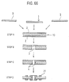
  • FIGS. 65 and 66 illustrate steps of an exemplary process of preparing a double side patterned substrate.
  • step A a prepreg sheet 1 of a predetermined thickness is sandwiched between a pair of copper (Cu) foils 2 of a predetermined thickness and lamination press.
  • step B through holes are drilled in the structure 10 (only one through hole 3 shown in FIG. 66).
  • step C copper (Cu) is plated to the through hole 3 to form a plating film 4.
  • step D both the copper foils 2 are patterned to form conductor patterns 21.
  • step E plating is effected for connection to external terminals as shown in FIG. 65.
  • the last-mentioned plating may be Ni plating followed by Pd plating, Ni plating followed by Au plating (plating may be either electrolytic or electroless plating), or carried out using a solder leveler.
  • FIGS. 67 and 68 illustrate steps of an exemplary process of preparing a multilayer substrate in which four layers are stacked.
  • step A a prepreg sheet 1 of a predetermined thickness is sandwiched between a pair of copper (Cu) foils 2 of a predetermined thickness and lamination press.
  • step B both the copper foils 2 are patterned to form conductor patterns 21.
  • step C on each of opposite surfaces of the double side patterned substrate thus obtained, a prepreg sheet 1 of a predetermined thickness and a copper foil 2 are placed, followed by simultaneous lamination press.
  • through holes are drilled in the structure (only one through hole 3 shown in FIG. 68).
  • step E copper (Cu) is plated to the through hole 3 to form a plating film 4.
  • step F both the outside copper foils 2 are patterned to form conductor patterns 21.
  • step G plating is effected for connection to external terminals as shown in FIG. 67.
  • the last-mentioned plating may be Ni plating followed by Pd plating, Ni plating followed by Au plating (plating may be either electrolytic or electroless plating), or carried out using a solder leveler.
  • the invention is not limited to the above-illustrated substrates, and a substrate of any desired structure can be formed.
  • a substrate of any desired structure can be formed using a substrate serving as a laminating press material, a copper foil-clad substrate and a prepreg, a multilayer structure can be formed while the prepreg serves as a bonding layer.
  • a paste of composite dielectric material or composite magnetic material obtained by milling the ceramic powder, magnetic powder, optional flame retardant and resin in a high-boiling solvent such as butylcarbitol acetate may be applied onto a patterned substrate by a screen printing or similar technique. This procedure is effective for improving characteristics.
  • Electronic parts can be fabricated by combining the prepreg, copper foil-clad substrate and multilayer substrate with a device design pattern and other constituent materials.
  • the electronic parts of the invention find use as capacitors, coils (or inductors), filters, etc.
  • the electronic parts can form antennas, and high-frequency electronic parts such as superposed modules for use in high-frequency electronic circuits such as RF modules, voltage controlled oscillators, and power amplifiers, as well as optical pickups.
  • the dielectric constant ⁇ and Q of composite material can be adjusted as desired by changing the type of resin and the type and content of dielectric powder blended therein.
  • the dielectric constant ⁇ and magnetic permeability ⁇ of composite material can be adjusted as desired by changing the type of resin and the type and content of magnetic powder blended therein.
  • FIGS. 1 and 2 illustrate an inductor according to a first embodiment of the invention.
  • FIG. 1 is a see-through perspective view and
  • FIG. 2 is a cross-sectional view.
  • the inductor 10 includes constituent layers (prepregs or substrates) 10a to 10e of composite resin materials, internal conductors (coil patterns) 13 formed on the constituent layers 10b to 10e, and via holes 14 for providing electrical connection to the internal conductors 13.
  • Via holes 14 can be formed by drilling, laser machining, etching or the like.
  • the ends of each coil formed are connected to through-vias 12 formed along end surfaces of the inductor 10 and land patterns 11 formed slightly above or below the through-vias 12.
  • Through-via 12 has a half-cut structure by dicing or V-cutting. This is because when a plurality of devices are formed in a collective substrate which is eventually cut into discrete pieces along lines at the centers of through-vias 12.
  • the constituent layers 10a to 10e of the inductor 10 should preferably have a dielectric constant of 2.6 to 3.5 because the distributed capacitance must be minimized for the potential application as a high-frequency chip inductor. Use of the above-mentioned organic dielectric layers is thus preferred. Separately, for an inductor constructing a resonance circuit, the distributed capacitance is sometimes positively utilized. In such application, the constituent layers should preferably have a dielectric constant of 5 to 40. Use of the above-mentioned first and second composite dielectric layers is thus preferred. In this way, it becomes possible to reduce the size of device and eliminate capacitive elements. Also in these inductors the material loss should be minimized.
  • the dielectric dissipation factor (tan ⁇ ) in the range of 0.0025 to 0.0075, an inductor having a minimized material loss and a high Q is obtainable.
  • the impedance must be maximized at the frequency of noise to be removed.
  • a magnetic permeability of 3 to 20 is appropriate, and use of the above-mentioned composite magnetic layers is preferred. This drastically improves the effect of removing high-frequency noise.
  • the respective constituent layers may be identical or different as long as constituent layers of at least two different types are included as a whole (the same applies in the following examples), and an optimum combination thereof may be selected.
  • FIG. 10A An equivalent circuit is shown in FIG. 10A. As seen from FIG. 10A, an electronic part (inductor) having a coil 31 is illustrated in the equivalent circuit.
  • FIGS. 3 and 4 illustrate an inductor according to a second embodiment of the invention.
  • FIG. 3 is a see-through perspective view and
  • FIG. 4 is a cross-sectional view.
  • Example 1 the coil pattern which is wound and stacked in a vertical direction in Example 1 is changed to a helical coil which is wound in a lateral direction.
  • the remaining components are the same as in Example 1.
  • the same components are designated by like numerals and their description is omitted.
  • FIGS. 5 and 6 illustrate an inductor according to a third embodiment of the invention.
  • FIG. 5 is a see-through perspective view and
  • FIG. 6 is a cross-sectional view.
  • Example 1 the coil pattern which is wound and stacked in a vertical direction in Example 1 is changed such that upper and lower spiral coils are connected.
  • the remaining components are the same as in Example 1.
  • the same components are designated by like numerals and their description is omitted.
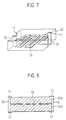
  • FIGS. 7 and 8 illustrate an inductor according to a fourth embodiment of the invention.
  • FIG. 7 is a see-through perspective view and
  • FIG. 8 is a cross-sectional view.
  • Example 1 the coil pattern which is wound and stacked in a vertical direction in Example 1 is changed to an internal meander coil.
  • the remaining components are the same as in Example 1.
  • the same components are designated by like numerals and their description is omitted.
  • FIG. 9 is a see-through perspective view of an inductor according to a fifth embodiment of the invention.
  • Example 1 the single coil in Example 1 is changed to an array of four juxtaposed coils. This array achieves a space saving.
  • the remaining components are the same as in Example 1.
  • the same components are designated by like numerals and their description is omitted.
  • the equivalent circuit is shown in FIG. 10B. As shown in FIG. 10B. an electronic part (inductor array) having four coils 31a to 31d is illustrated in the equivalent circuit.
  • FIGS. 11 and 12 illustrate a capacitor according to a sixth embodiment of the invention.
  • FIG. 11 is a see-through perspective view and
  • FIG. 12 is a cross-sectional view.
  • the capacitor 20 includes constituent layers (prepregs or substrates) 20a to 20g of composite resin materials, internal conductors (internal electrode patterns) 23 formed on the constituent layers 20b to 20g, through-vias 22 formed along end surfaces of the capacitor 20 and alternately connected to the internal conductors 23, and land patterns 21 formed slightly above or below the through-vias 22.
  • the constituent layers 20a to 20g of the capacitor 20 should preferably have a dielectric constant of 2.6 to 40 and a dielectric dissipation factor of 0.0025 to 0.0075 when the diversity and precision of capacitance are considered. Then a choice may be made among the above-mentioned organic dielectric layers or the above-mentioned first and second composite dielectric layers. This enables to provide a wider range of capacitance and afford even a low capacitance at a high precision. It is also required that the material loss be minimized. By setting the dielectric dissipation factor (tan ⁇ ) in the range of 0.0075 to 0.025, a capacitor having a minimized material loss is obtainable.
  • the respective constituent layers may be identical or different and an optimum combination thereof may be selected.
  • the equivalent circuit is shown in FIG. 14A. As shown in FIG. 14A, an electronic part (capacitor) having a capacitance 32 is illustrated in the equivalent circuit.
  • FIG. 13 is a see-through perspective view of a capacitor according to a seventh embodiment of the invention.
  • Example 6 the single capacitor in Example 6 is changed to an array of four juxtaposed capacitors.
  • capacitors When capacitors are formed in an array, it sometimes occurs to provide different capacitances at a high precision.
  • the above-mentioned ranges of dielectric constant and dielectric dissipation factor are preferable.
  • the remaining components are the same as in Example 6.
  • the same components are designated by like numerals and their description is omitted.
  • the equivalent circuit is shown in FIG. 14B. As shown in FIG. 14B, an electronic part (capacitor array) having four capacitors 32a to 32d is illustrated in the equivalent circuit.
  • FIGS. 15 to 18 illustrate a balun transformer according to an eighth embodiment of the invention.
  • FIG. 15 is a see-through perspective view
  • FIG. 16 is a cross-sectional view
  • FIG. 17 is an exploded plan view of respective constituent layers
  • FIG. 18 is an equivalent circuit diagram.
  • the balun transformer 40 includes a stack of constituent layers 40a to 400 of composite resin materials, internal GND conductors 45 disposed above, below and intermediate the stack, and internal conductors 43 formed between the internal GND conductors 45.
  • the internal conductors 43 are spiral conductor sections 43 having a length of ⁇ g/4 which are connected by via holes 44 so as to construct coupling lines 53a to 53d as shown in the equivalent circuit of FIG. 18.
  • the constituent layers 40a to 40o of the balun transformer 40 should preferably have a dielectric constant of 2.6 to 40 and a dielectric dissipation factor (tan ⁇ ) of 0.0075 to 0.025. Then a choice may be made among the above-mentioned organic dielectric layers or the above-mentioned first and second composite dielectric layers. In some applications wherein a magnetic permeability of 3 to 20 is appropriate, use of the above-mentioned composite magnetic layers is preferred.
  • the respective constituent layers may be identical or different and an optimum combination thereof may be selected.
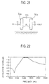
  • FIGS. 19 to 22 illustrate a multilayer filter according to a ninth embodiment of the invention.
  • FIG. 19 is a perspective view.
  • FIG. 20 is an exploded perspective view,
  • FIG. 21 is an equivalent circuit diagram, and
  • FIG. 22 is a transmission diagram.
  • the multilayer filter is constructed as having two poles.
  • the multilayer filter 60 includes a stack of constituent layers 60a to 60e, a pair of strip lines 68 and a pair of capacitor conductors 67 both disposed approximately at the center of the stack.
  • the capacitor conductors 67 are formed on a lower constituent layer group 60d, and the strip lines 68 are formed on a constituent layer 60c thereon.
  • GND conductors 65 are formed on upper and lower end surfaces of the constituent layers 60a to 60e so that the strip lines 68 and capacitor conductors 67 are interleaved therebetween.
  • the strip lines 68, capacitor conductors 67 and GND conductors 65 are connected to end electrodes (external terminals) 62 formed on end sides and land patterns 61 formed slightly above or below the end electrodes 62.
  • GND patterns 66 which are formed on opposite sides and slightly above or below therefrom are connected to GND conductors 65.
  • the strip lines 68 are strip lines 74a, 74b having a length of ⁇ g/4 or shorter as shown in the equivalent circuit of FIG. 21.
  • the capacitor conductors 67 constitute input and output coupling capacitances Ci.
  • the strip lines 74a and 74b are coupled by a coupling capacitance Cm and a coupling coefficient M.
  • Such an equivalent circuit indicates the implementation of a multilayer filter having transmission characteristics of the two pole type as shown in FIG. 22.
  • the multilayer filter 60 exhibits desired transmission characteristics in a frequency band of several hundreds of megahertz to several gigahertz when the constituent layers 60a to 60e have a dielectric constant of 2.6 to 40. It is desired to minimize the material loss of the strip line resonator, and hence, setting a dielectric dissipation factor (tan ⁇ ) in the range of 0.0025 to 0.0075 is preferable. Then a choice may be made among the above-mentioned organic dielectric layers or the above-mentioned first and second composite dielectric layers. The respective constituent layers may be identical or different and an optimum combination thereof may be selected.
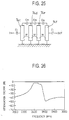
  • FIGS. 23 to 26 illustrate a multilayer filter according to a tenth embodiment of the invention.
  • FIG. 23 is a perspective view
  • FIG. 24 is an exploded perspective view
  • FIG. 25 is an equivalent circuit diagram
  • FIG. 26 is a transmission diagram.
  • the multilayer filter is constructed as having four poles.
  • the multilayer filter 60 includes a stack of constituent layers 60a to 60e, four strip lines 68 and a pair of capacitor conductors 67 both disposed approximately at the center of the stack.
  • the four pole arrangement enables to produce sharp transmission characteristics as shown in FIG. 26.
  • the remaining components are the same as in Example 9. The same components are designated by like numerals and their description is omitted.
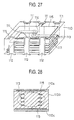
  • FIGS. 27 to 31 illustrate a coupler according to an 11th embodiment of the invention.
  • FIG. 27 is a perspective view
  • FIG. 28 is a cross-sectional view
  • FIG. 29 is an exploded perspective view of respective constituent layers
  • FIG. 30 is a diagram of internal connection
  • FIG. 31 is an equivalent circuit diagram.
  • the coupler 110 includes a stack of constituent layers 110a to 110c of composite resin materials, internal GND conductors 115 formed and disposed on the top and bottom of the stack, and internal conductors 113 formed between the internal GND conductors 115.
  • the internal conductors 113 are connected by via holes 114 in a spiral fashion so that two coils construct a transformer. Ends of the thus formed coils and internal GND conductors 115 are connected to through-vias 112 formed on end sides and land patterns 111 formed slightly above or below the through-vias 112 as shown in FIG. 30.
  • a coupler 110 having two coils 125a and 125b coupled is obtained as shown in the equivalent circuit diagram of FIG. 31.
  • the constituent layers 110a to 110c of the coupler 110 should preferably have a minimized dielectric constant.
  • a higher dielectric constant is desirable. Therefore, depending on the intended application, required performance and specifications, a material having an appropriate dielectric constant may be used. In most oases, setting a dielectric constant in the range of 2.6 to 40 ensures desired transmission characteristics in a band of several hundreds of megahertz to several gigahertz.
  • a dielectric dissipation factor (tan ⁇ ) of 0.0025 to 0.0075 is preferable.
  • This choice enables to form an inductor having a minimized material loss and a high Q value, leading to a high performance coupler. Then a choice may be made among the above-mentioned organic dielectric layers or the above-mentioned first and second composite dielectric layers.
  • the respective constituent layers may be identical or different and an optimum combination thereof may be selected.
  • FIGS. 32 to 34 illustrate an antenna according to a 12th embodiment of the invention.
  • FIG. 32 is a see-through perspective view
  • FIG. 33A is a plan view
  • FIG. 33B is a cross-sectional elevational view
  • FIG. 33C is a cross-sectional end view
  • FIG. 34 is an exploded perspective view of respective constituent layers.
  • the antenna 130 includes a stack of constituent layers (prepregs or substrates) 130a to 130c of composite resin materials, and internal conductors (antenna patterns) 133 formed on constituent layers 130b and 130c. Ends of the internal conductors 133 are connected to through-vias 132 formed at end sides of the antenna and land patterns 131 formed slightly above and below the through-vias 132.
  • the internal conductor 133 is constructed as a reactance element having a length of about ⁇ g/4 at the operating frequency and formed in a meander fashion.
  • the constituent layers 130a to 130c of the antenna 130 should preferably have a minimized dielectric constant.
  • a higher dielectric constant is desirable. Therefore, depending on the intended application, required performance and specifications, a material having an appropriate dielectric constant may be used. In most cases, a dielectric constant in the range of 2.6 to 40 and a dielectric dissipation factor (tan ⁇ ) of 0.0075 to 0.025 are preferable. Then a choice may be made among the above-mentioned organic dielectric layers or the above-mentioned first and second composite dielectric layers. This choice enables to spread the frequency range and increase the precision of formation. It is also necessary to minimize the material loss.
  • a dielectric dissipation factor (tans) 0.0025 to 0.0075
  • an antenna having a minimum material loss is achievable.
  • the respective constituent layers may be identical or different and an optimum combination thereof may be selected.
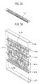
  • FIGS. 35 and 36 illustrate an antenna according to a 13th embodiment of the invention.
  • FIG. 35 is a see-through perspective view
  • FIG. 36 is an exploded perspective view of respective constituent layers.
  • the antenna in this example is constructed as an antenna having a helical internal electrode.
  • the antenna 140 includes a stack of constituent layers (prepregs or substrates) 140a to 140c of composite resin materials, and internal conductors (antenna patterns) 143a, 143b formed on constituent layers 140b and 140c.
  • the upper and lower internal conductors 143a and 143b are connected by via holes 144 to form a helical inductance device.
  • the remaining components are the same as in Example 12. The same components are designated by like numerals and their description is omitted.
  • FIGS. 37 and 38 illustrate a patch antenna according to a 14th embodiment of the invention.
  • FIG. 37 is a see-through perspective view
  • FIG. 38 is a cross-sectional view.
  • the patch antenna 150 includes a constituent layer (prepreg or substrate) 150a of composite resin material, a patch conductor (antenna pattern) 159 formed on the top of constituent layer 150a, and a GND conductor 155 formed on the bottom of constituent layer 150a so as to oppose to the patch conductor 159.
  • a power supply through conductor 154 is connected to the patch conductor 159 at a power supply site 153.
  • An annular gap 156 is provided between the through conductor 154 and the GND conductor 155 so that the through conductor 154 may not be connected to the GND conductor 155. Then power supply is provided from below the GND conductor 155 via the through conductor 154.
  • the constituent layer 150a of the patch antenna 150 should preferably have a minimized dielectric constant.
  • a higher dielectric constant is desirable. Therefore, depending on the intended application, required performance and specifications, a material having an appropriate dielectric constant may be used. In most cases, a dielectric constant in the range of 2.6 to 40 and a dielectric dissipation factor (tan ⁇ ) of 0.0075 to 0.025 are preferable. Then a choice may be made among the above-mentioned organic dielectric layers or the above-mentioned first and second composite dielectric layers. This choice enables to spread the frequency range and increase the precision of formation. It is also necessary to minimize the material loss. By setting a dielectric dissipation factor (tan ⁇ ) of 0.0025 to 0.0075, an antenna having a minimum material loss and a high radiation efficiency is achievable.
  • a magnetic material exerts a wavelength reducing effect as a dielectric material does, which enables to increase the inductance of a radiation element.
  • a high Q value is available even at a relatively low frequency.
  • a magnetic permeability of 3 to 20 is preferable in some applications and use of the above-mentioned composite magnetic layers is preferred. This enables performance improvement and size reduction in a frequency band of less than several hundreds of megahertz.
  • the respective constituent layers may be identical or different and an optimum combination thereof may be selected.
  • the patch antenna becomes easy to design if the dielectric constant of the base substrate is finely adjustable.
  • the use of many materials having different dielectric constants is awkward to manage. It is then recommended to combine several materials having different dielectric constants (to form a multilayer structure) so as to tailor the dielectric constant of the entire structure. This enables fine adjustment of a dielectric constant, increases the degree of freedom of design, and facilitates the design. An antenna featuring small size and high performance is obtainable.
  • FIGS. 39 and 40 illustrate a patch antenna according to a 15th embodiment of the invention.
  • FIG. 39 is a see-through perspective view
  • FIG. 40 is a cross-sectional view.
  • the patch antenna 160 includes a constituent layer (prepreg or substrate) 160a of composite resin material, a patch conductor (antenna pattern) 169 formed on the top of constituent layer 160a, and a GND conductor 165 formed on the bottom of constituent layer 160a so as to oppose to the patch conductor 169.
  • a power supply conductor 161 is provided near the patch conductor 169, but spaced therefrom. Power supply is provided to the power supply conductor 161 via a power supply terminal 162.
  • the power supply terminal 162 may be formed from copper, gold, palladium, platinum, aluminum or the like by effecting suitable treatment such as plating, termination, printing, sputtering or evaporation.
  • the remaining components are the same as in Example 14. The same components are designated by like numerals and their description is omitted.
  • FIGS. 41 and 42 illustrate a patch antenna according to a 16th embodiment of the invention.
  • FIG. 41 is a see-through perspective view
  • FIG. 42 is a cross-sectional view.
  • the patch antenna 170 includes constituent layers (prepregs or substrates) 150a, 150b of composite resin materials, patch conductors 159a, 159e formed on the constituent layers 150a, 150b, and a GND conductor 155 formed on the bottom of constituent layer 150b so as to oppose to the patch conductors 159a, 159e.
  • a power supply through conductor 154 is connected to the patch conductor 159a at a power supply site 153a.
  • a gap 156 is provided between the through conductor 154 and the GND conductor 155 and patch conductor 159e so that the through conductor 154 may not be connected to the GND conductor 155 and patch conductor 159e.
  • FIGS. 43 and 44 illustrate a multi-array patch antenna according to a 17th embodiment of the invention.
  • FIG. 43 is a see-through perspective view
  • FIG. 44 is a cross-sectional view.
  • the array includes constituent layers 150a, 150b of composite resin materials, patch conductors 159a, 159b, 159c, 159d formed on the constituent layer 150a, patch conductors 159e, 159f, 159g, 159h formed on the constituent layer 150b, and a GND conductor 155 formed on the bottom of the constituent layer 150b so as to oppose to the patch conductors 159a, 159e.
  • the remaining components are the same as in Example 16. The same components are designated by like numerals and their description is omitted.
  • the array formation enables to reduce the size of a set and the number of parts.
  • FIGS. 45 to 47 illustrate a voltage controlled oscillator (VCO) according to an 18th embodiment of the invention.
  • FIG. 45 is a see-through perspective view
  • FIG. 46 is a cross-sectional view
  • FIG. 47 is an equivalent circuit diagram.
  • the VCO includes a stack of constituent layers 210a to 210g of composite resin materials, electronic parts 261 disposed and formed on the stack including capacitors, inductors, semiconductors and registers, and conductor patterns 262, 263, 264 formed above, below and intermediate the constituent layers 210a to 210g. Since the VCO is constructed to an equivalent circuit as shown in FIG. 47, it further includes strip lines 263, capacitors, signal lines, semiconductors and power supply lines. It is advantageous to form the respective constituent layers from materials selected appropriate for their function.
  • first or second composite dielectric layers having a dielectric dissipation factor of 0.0025 to 0.0075.
  • first or second composite dielectric layers so as to give a dielectric dissipation factor of 0.0075 to 0.025 and a dielectric constant of 5 to 40.
  • organic dielectric layers having a dielectric dissipation factor of 0.0025 to 0.0075 and a dielectric constant of 2.6 to 3.5.
  • constituent layers 210a to 210g there are provided internal conductors including strip line 263, GND conductor 262, capacitor conductor 264, wiring inductor conductor 265 and terminal conductor 266. Upper and lower internal conductors are connected by via holes 214. Electronic parts 261 are mounted on the surface, completing a VCO corresponding to the equivalent circuit of FIG. 47.
  • This construction enables to provide an appropriate dielectric constant, Q and dielectric dissipation factor for a distinct function, arriving at a high performance, small size, and thin part.
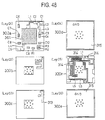
  • FIGS. 48 to 50 illustrate a power amplifier according to a 19th embodiment of the invention.
  • FIG. 48 is an exploded plan view of respective constituent layers
  • FIG. 49 is a cross-sectional view
  • FIG. 50 is an equivalent circuit diagram.
  • the power amplifier includes a stack of constituent layers 300a to 300e, electronic parts 361 formed thereon including capacitors, inductors, semiconductors and registers, and conductor patterns 313, 315 formed above, below and intermediate the constituent layers 300a to 300e. Since the power amplifier is constructed to an equivalent circuit as shown in FIG. 50, it further includes strip lines L11 to L17, capacitors C11 to C20, signal lines, and power supply lines to semiconductor devices. It is advantageous to form the respective constituent layers from materials selected appropriate for their function.
  • first or second composite dielectric layers having a dielectric dissipation factor of 0.0075 to 0.025 and a dielectric constant of 2.6 to 40.
  • first or second composite dielectric layers so as to give a dielectric dissipation factor of 0.0075 to 0.025 and a dielectric constant of 5 to 40.
  • This construction enables to provide an appropriate dielectric constant, Q and dielectric dissipation factor for a distinct function, arriving at a high performance, small size, and thin part.
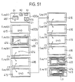
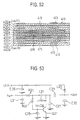
  • FIGS. 51 to 53 illustrate a superposed module according to a 20th embodiment of the invention, the module finding use as an optical pickup or the like.
  • FIG. 51 is an exploded plan view of respective constituent layers
  • FIG. 52 is a cross-sectional view
  • FIG. 53 is an equivalent circuit diagram.
  • the superposed module includes a stack of constituent layers 400a to 400k, electronic parts 461 formed thereon including capacitors, inductors, semiconductors and registers, and conductor patterns 413, 415 formed above, below and intermediate the constituent layers 400a to 400k. Since the superposed module is constructed to an equivalent circuit as shown in FIG. 53, it further includes inductors L21, L23, capacitors C21 to C27, signal lines, and power supply lines to semiconductor devices. It is advantageous to form the respective constituent layers from materials selected appropriate for their function.
  • second composite dielectric layers so as to give a dielectric dissipation factor of 0.0075 to 0.025 and a dielectric constant of 10 to 40.
  • organic dielectric layers having a dielectric dissipation factor of 0.0025 to 0.0075 and a dielectric constant of 2.6 to 3.5.
  • This construction enables to provide an appropriate dielectric constant, Q and dielectric dissipation factor for a distinct function, arriving at a high performance, small size, and thin part.
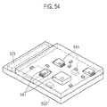
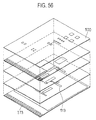
  • FIGS. 54 to 57 illustrate a RF module according to a 21st embodiment of the invention.
  • FIG. 54 is a perspective view
  • FIG. 55 is a perspective view with an outer housing removed
  • FIG. 56 is an exploded perspective view of respective constituent layers
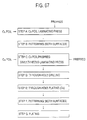
  • FIG. 57 is a cross-sectional view.
  • the RF module includes a stack of constituent layers 500a to 500i, electronic parts 561 formed and disposed thereon including capacitors, inductors, semiconductors and registers, conductor patterns 513. 515, 572 formed above, below and intermediate the constituent layers 500a to 500i, and an antenna pattern 573.
  • the RF module includes inductors, capacitors, signal lines, and power supply lines to semiconductor devices. It is advantageous to form the respective constituent layers from materials selected appropriate for their function.
  • constituent layers 500d to 500d, 500g constructing the antenna, strip lines and wiring in this example it is preferred to use organic dielectric layers having a dielectric dissipation factor of 0.0025 to 0.0075 and a dielectric constant of 2.6 to 3.5.
  • organic dielectric layers having a dielectric dissipation factor of 0.0025 to 0.0075 and a dielectric constant of 2.6 to 3.5.
  • second composite dielectric layers so as to give a dielectric dissipation factor of 0.0075 to 0.025 and a dielectric constant of 10 to 40.
  • composite magnetic layers having a magnetic permeability of 3 to 20.
  • This construction enables to provide an appropriate dielectric constant, Q and dielectric dissipation factor for a distinct function, arriving at a high performance, small size, and thin part.
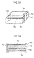
  • FIGS. 58 and 59 illustrate a strip resonator according to a 22nd embodiment of the invention.
  • FIG. 58 is a see-through perspective view
  • FIG. 59 is a cross-sectional view.
  • the strip resonator includes an intermediate rectangular strip conductor 784, upper and lower rectangular GND conductors 783, and constituent layers 710 sandwiched therebetween.
  • a HOT terminal 781 and a GND terminal 782 for a resonator are formed and connected.
  • the method of forming the remaining components is the same as in the inductor of Example 1.
  • a dielectric dissipation factor (tan ⁇ ) of 0.0025 to 0.0075 is preferred. Then a choice is preferably made of the above-mentioned organic dielectric layers or first or second composite dielectric layers.
  • FIG. 60 is a see-through perspective view of a strip resonator according to a 23rd embodiment of the invention.
  • the strip resonator in FIG. 60 includes an intermediate U-shaped strip conductor 884, upper and lower rectangular GND conductors 883, and constituent layers 810 sandwiched therebetween.
  • a HOT terminal 881 and a GND terminal 882 for a resonator are formed and connected.
  • the method of forming the remaining components is the same as in the inductor of Example 1.
  • a dielectric dissipation factor (tan ⁇ ) of 0.0025 to 0.0075 is preferred. Then a choice is preferably made of the above-mentioned organic dielectric layers or first or second composite dielectric layers.
  • FIG. 61 is an equivalent circuit diagram of the resonators in the foregoing Examples 22 and 23.
  • a HOT terminal 981 for the resonator is connected to one end of a resonator 984, 941 constructed by a coaxial path or strip line, and a GND terminal 982 is connected to the other end thereof.
  • FIG. 62 is a block diagram showing a high-frequency portion of a portable terminal equipment according to a 24th embodiment of the invention.
  • a base band unit 1010 delivers a transmission signal to a mixer 1001 where the signal is mixed with an RF signal from a hybrid circuit 1021.
  • a voltage controlled oscillator (VCO) 1020 is connected to the hybrid circuit 1021 to construct a synthesizer circuit with a phase lock loop circuit 1019 so that the hybrid circuit 1021 may deliver an RF signal of a predetermined frequency.
  • VCO voltage controlled oscillator
  • the transmission signal which has been RF modulated by the mixer 1001 is passed through a band-pass filter (BPF) 1002 and amplified by a power amplifier 1003.
  • BPF band-pass filter
  • An output of the power amplifier 1003 is partially taken out of a coupler 1004, adjusted to a predetermined level by an attenuator 1005, and fed back to the power amplifier 1003 for adjusting so that the power amplifier may have a constant gain.
  • the coupler 1004 delivers a transmission signal to a duplexer 1008 through an isolator 1006 for precluding reverse current and a low-pass filter 1007.
  • the signal is transmitted from an antenna 1009 connected to the duplexer 1008.
  • An input signal received by the antenna 1009 is fed from the duplexer 1008 to an amplifier 1011 and amplified to a predetermined level.
  • the received signal delivered from the amplifier 1011 is fed to a mixer 1013 through a band-pass filter 1012.
  • the mixer 1013 receives an RF signal from the hybrid circuit 1021 whereby the RF signal component is removed to effect demodulation.
  • the received signal delivered from the mixer 1013 is passed through a SAW filter 1014, amplified by an amplifier 1015, and fed to a mixer 1016.
  • the mixer 1016 also receives a local transmission signal of a predetermined frequency from a local transmitter circuit 1018.
  • the received signal is converted to a desired frequency, amplified to a predetermined level by an amplifier 1017 and sent to the base band unit 1010.
  • an antenna front end module 1200 including the antenna 1009, duplexer 1008, and low-pass filter 1007, and an isolator power amplifier module 1100 including the isolator 1006, coupler 1004, attenuator 1005 and power amplifier 1003 can be constructed as a hybrid module by the same procedure as above. Further, a unit including other components can be constructed as an RF unit as demonstrated in Example 21. BPF, VCO, etc. can be constructed in accordance with the procedures shown in Examples 9 to 11 and 18.
  • the invention is also applicable by a similar procedure to coil cores, troidal cores, disk capacitors, lead-through capacitors, clamp filters, common mode filters, EMC filters, power supply filters, pulse transformers, deflection coils, choke coils, DC-DC converters, delay lines, diplexers, duplexers, antenna switch modules, antenna front end modules, isolator/power amplifier modules, PLL modules, front end modules, tuner units, directional couplers, double balanced mixers (DBM), power synthesizers, power distributors, toner sensors, current sensors, actuators, sounders (piezoelectric sound generators), microphones, receivers, buzzers, PTC thermistors, temperature fuses, ferrite magnets, etc.
  • DBM double balanced mixers
  • any of flame retardants for example, halides such as halogenated phosphates and brominated epoxy resins, organic compounds such as phosphate amides, and inorganic materials such as antimony trioxide and aluminum hydride may be added to the constituent layers.
  • halides such as halogenated phosphates and brominated epoxy resins
  • organic compounds such as phosphate amides
  • inorganic materials such as antimony trioxide and aluminum hydride
  • the invention provides high-frequency electronic parts having improved high-frequency characteristics and hence, improved overall electrical characteristics.

Landscapes

  • Engineering & Computer Science (AREA)
  • Power Engineering (AREA)
  • Coils Or Transformers For Communication (AREA)
  • Laminated Bodies (AREA)
  • Ceramic Capacitors (AREA)
  • Fixed Capacitors And Capacitor Manufacturing Machines (AREA)
  • Production Of Multi-Layered Print Wiring Board (AREA)

Abstract

Using plural layers selected from among composite resin substrates having a fully high or low dielectric constant, composite resin substrates having a fully high magnetic permeability, and composite resin substrate layers having a fully high Q value, the invention provides a multilayer electronic part of small size having high performance and improved overall electrical characteristics. The multilayer electronic part includes constituent layers of at least two types formed of composite materials and a conductor layer formed on at least one composite material layer, wherein the conductor layer constructs a predetermined electric circuit.

Description

This invention relates to electronic parts and multilayer circuits using prepreg and substrate, and more particularly, to such electronic parts suitable for operation in a high frequency region of at least 100 MHz and for use in magnetic characteristics-utilizing applications and magnetic shields.
BACKGROUND OF THE INVENTION
In the field of electronic equipment for communication, commercial and industrial applications, the current mounting technology seeks further miniaturization and higher density packaging. Concomitant with this trend, materials are required to have better heat resistance, dimensional stability, electrical characteristics and moldability.
Known electronic parts or multilayer substrates for high frequency operation include sintered ferrite and sintered ceramics which are laminated and molded into substrate form. Laminating such materials into multilayer substrates has been practiced in the art because of the_ advantage of potential miniaturization.
The use of sintered ferrite and sintered ceramics, however, gives rise to several problems. A number of steps are involved in firing and thick film printing. Sintered materials suffer from inherent defects including cracks and warp caused by firing. Cracks are also induced by the differential thermal expansion between sintered material and printed circuit board. It is thus increasingly required to replace the sintered materials by resinous materials.
With resinous materials as such, however, a satisfactory dielectric constant is arrived at with great difficulty, and little improvement in magnetic permeability is achievable. Then, electronic parts utilizing resinous materials as such fail to provide satisfactory characteristics and become large in size, rendering it difficult to reduce the size and thickness of electronic parts.
It is also known from JP-A 8-69712 and JP-A 11-192620 to mix resinous materials with ceramic powder into composite materials. These composite materials, however, have unsatisfactory high-frequency characteristics and magnetic characteristics.
Also, JP-B 6-14600 discloses the sheeting technique of forming plural materials into layers, followed by lamination. This method involves a number of steps. The operating frequency of the multilayer part referred to in this patent is several megahertz at maximum. No study is made on the performance of the multilayer part in the high-frequency region of at least 100 MHz.
SUMMARY OF THE INVENTION
An object of the invention is to provide a multilayer electronic part having the advantages of small size, excellent performance and improved overall electrical characteristics, using plural layers selected from among composite resin substrates having a sufficiently high or low dielectric constant, composite resin substrates having a sufficiently high dielectric constant, and composite resin substrate layers having a sufficiently high Q value.
According to the invention, there is provided a multilayer electronic part comprising constituent layers of at least two types formed of hybrid or composite materials and a conductor layer formed on at least one composite material layer, the conductor layer constructing a predetermined electric circuit.
The multilayer electronic part is typically used in a frequency band of at least 100 MHz. Preferably the constituent layers include a layer containing at least reinforcing fibers. Also preferably, the constituent layers include at least one layer containing at least one flame retardant.
In a first preferred embodiment, the constituent layers include at least one first composite dielectric layer in which a dielectric powder having a dielectric constant (or relative permittivity) of 5 to 10,000 and a dielectric dissipation factor of 0.00002 to 0.01 is dispersed in an amount of 10 to 65% by volume such that the first composite dielectric layer has a dielectric constant of 5 to 20 and a dielectric dissipation factor of 0.0025 to 0.0075.
In a second preferred embodiment, the constituent layers include at least one second composite dielectric layer in which a dielectric powder having a dielectric constant of 20 to 20,000 and a dielectric dissipation factor of 0.01 to 0.0001 is dispersed in an amount of 10 to 65% by volume such that the second composite dielectric layer has a dielectric constant of 10 to 40 and a dielectric dissipation factor of 0.0075 to 0.025.
In a third preferred embodiment, the constituent layers include at least one composite magnetic layer in which a magnetic powder is dispersed in an amount of 10 to 65% by volume such that the composite magnetic layer has a magnetic permeability of 3 to 20.
According to the invention, multilayer substrates are constructed using a composite material of at least a resin and a magnetic powder and a composite material of at least a resin and a dielectric powder. There can be obtained magnetic substrates having a low dielectric constant and excellent high-frequency characteristics and dielectric substrates having excellent high-frequency characteristics. As a consequence, a multilayer electronic part having excellent overall high-frequency characteristics is obtainable.
BRIEF DESCRIPTION OF THE DRAWINGS
  • FIGS. 1 and 2 illustrate an inductor as one exemplary electronic part of the invention.
  • FIGS. 3 and 4 illustrate an inductor as another exemplary electronic part of the invention.
  • FIGS. 5 and 6 illustrate an inductor as a further exemplary electronic part of the invention.
  • FIGS. 7 and 8 illustrate an inductor as a still further exemplary electronic part of the invention.
  • FIG. 9 illustrates an inductor as a yet further exemplary electronic part of the invention.
  • FIGS. 10A and 10B are equivalent circuit diagrams of the inductors.
  • FIGS. 11 and 12 illustrate a capacitor as one exemplary electronic part of the invention.
  • FIG. 13 illustrates a capacitor as another exemplary electronic part of the invention.
  • FIGS. 14A and 14B are equivalent circuit diagrams of the capacitors.
  • FIGS. 15 to 17 illustrate a balun transformer as one exemplary electronic part of the invention.
  • FIG. 18 is an equivalent circuit diagram of the balun transformer.
  • FIGS. 19 and 20 illustrate a multilayer filter as one exemplary electronic part of the invention.
  • FIG. 21 is an equivalent circuit diagram of the multilayer filter.
  • FIG. 22 is a graph showing transmission characteristics of the multilayer filter.
  • FIGS. 23 and 24 illustrate a multilayer filter as another exemplary electronic part of the invention.
  • FIG. 25 is an equivalent circuit diagram of the multilayer filter.
  • FIG. 26 is a graph showing transmission characteristics of the multilayer filter.
  • FIGS. 27 to 29 illustrate a coupler as one exemplary electronic part of the invention.
  • FIG. 30 illustrates the internal connections of the coupler.
  • FIG. 31 is an equivalent circuit diagram of the coupler.
  • FIGS. 32 to 34 illustrate an antenna as one exemplary electronic part of the invention.
  • FIGS. 35 and 36 illustrate an antenna as another exemplary electronic part of the invention.
  • FIGS. 37 and 38 illustrate a patch antenna as one exemplary electronic part of the invention.
  • FIGS. 39 and 40 illustrate a patch antenna as another exemplary electronic part of the invention.
  • FIGS. 41 and 42 illustrate a patch antenna as a further exemplary electronic part of the invention.
  • FIGS. 43 and 44 illustrate a patch antenna as a still further exemplary electronic part of the invention.
  • FIGS. 45 and 46 illustrate a VCO as one exemplary electronic part of the invention.
  • FIG. 47 is an equivalent circuit diagram of the VCO.
  • FIGS. 48 and 49 illustrate a power amplifier as one exemplary electronic part of the invention.
  • FIG. 50 is an equivalent circuit diagram of the power amplifier.
  • FIGS. 51 and 52 illustrate a superposed module as one exemplary electronic part of the invention.
  • FIG. 53 is an equivalent circuit diagram of the superposed module.
  • FIGS. 54 to 57 illustrate an RF unit as one exemplary electronic part of the invention, FIG. 54 being a perspective view of the unit, FIG. 55 being a perspective view of the substrate, FIG. 56 being an exploded perspective view, and FIG. 57 being a cross-sectional view.
  • FIGS. 58 and 59 illustrate a resonator as one exemplary electronic part of the invention.
  • FIG. 60 illustrates a resonator as another exemplary electronic part of the invention.
  • FIG. 61 is an equivalent circuit diagram of the resonator.
  • FIG. 62 is a block diagram showing a high-frequency portion of a portable equipment as one exemplary electronic part of the invention.
  • FIGS. 63A to 63D illustrate steps of a process for forming a copper foil-clad substrate.
  • FIGS. 64A to 64D illustrate steps of another process for forming a copper foil-clad substrate.
  • FIG. 65 illustrates steps of a further process for forming a copper foil-clad substrate.
  • FIG. 66 illustrates steps of a process for forming a multilayer substrate.
  • FIGS. 67/8 illustrates steps of another process for forming a multilayer substrate.
  • DESCRIPTION OF THE PREFERRED EMBODIMENT
    The multilayer electronic part of the invention includes at least two different constituent layers formed of hybrid or composite materials and a conductor layer formed on at least one composite material layer. A predetermined electric circuit is constructed by the conductor layer.
    This construction enables to adjust a dielectric constant ε and to provide a lower dielectric constant so that the part is suited for use in the high-frequency region of at least 100 MHz, and especially 100 MHz to 10 GHz. The composite magnetic material layers are suitable for use in magnetic characteristic-utilizing applications and as magnetic shields. On the other hand, the composite dielectric material layers can provide a relatively high Q and ε value in the high-frequency band, and yields a composite dielectric material substrate suited for use in the application where such characteristics are required, for example, such electronic parts as strip lines, impedance matching circuits, delay circuits, and antennas. High strength is another advantage.
    When substrates or multilayer electronic parts are fabricated using the composite magnetic material layers or composite dielectric material layers, the invention enables bonding with copper foil without a need for adhesive. patterning, and lamination. Such patterning and lamination can be conducted through the same steps as conventional substrate manufacturing steps, contributing to a cost reduction and efficient manufacture. Electronic parts using the thus fabricated substrates have a high strength and improved high-frequency characteristics.
    The invention is now described in further detail.
    The resin used in the multilayer electronic part is not critical. A proper choice may be made among resin materials having good moldability, processability, adhesion during stacking, and electrical characteristics. Specifically, thermosetting resins and thermoplastic resins are preferred.
    The thermosetting resins which can be used herein include epoxy resins, phenolic resins, unsaturated polyester resins, vinyl ester resins, polyimide resins, polyphenylene ether (or oxide) resins, bismaleimide triazine (or cyanate) resins, fumarate resins, and polybutadiene resins. The thermoplastic resins which can be used herein include aromatic polyester resins, polyphenylene sulfide resins, polyethylene terephthalate resins, polybutylene terephthalate resins, polyethylene sulfide resins, polyether ether ketone resins, polytetrafluoroethylene resins, and graft resins. Among these, phenolic resins, epoxy resins, low dielectric constant epoxy resins, polybutadiene resins, and BT resins are preferred as the base resin.
    These resins may be used alone or in admixture of two or more. Mixtures may have any desired mixing ratio of two or more resin components.
    The multilayer electronic part preferably has at least one organic dielectric layer formed of the above resin and having a dielectric constant of 2.4 to 4.5 and a dielectric dissipation factor of 0.002 to 0.03. Such an organic dielectric layer is especially suited in forming inductor devices such as coils since it can minimize the distributed capacitance.
    In one preferred embodiment, the multilayer electronic part includes at least one first composite dielectric layer in which a dielectric powder having a dielectric constant of 5 to 10,000 and a dielectric dissipation factor of 0.01 to 0.00002 is dispersed in the resin in an amount of 10 to 65% by volume such that the first composite dielectric layer has a dielectric constant of 5 to 20 and a dielectric dissipation factor of 0.0025 to 0.0075. This embodiment provides an adequate dielectric constant and a high Q value and hence, a reduced transmission loss, and is suitable in forming such electronic circuits as balun (balanced-and-unbalanced) transformers, antennas and power amplifiers.
    In another preferred embodiment, the multilayer electronic part includes at least one second composite dielectric layer in which a dielectric powder having a dielectric constant of 20 to 20,000 and a dielectric dissipation factor of 0.05 to 0.0001 is dispersed in the resin in an amount of 10 to 65% by volume such that the second composite dielectric layer has a dielectric constant of 10 to 40 and a dielectric dissipation factor of 0.0075 to 0.025. This embodiment provides an adequate Q value and a high dielectric constant, and is suitable in forming such electronic circuits as capacitors, patch antennas, voltage controlled oscillators (VCO) and power amplifiers.
    In a further preferred embodiment, the multilayer electronic part includes at least one composite magnetic layer in which a magnetic powder is dispersed in the resin in an amount of 10 to 65% by volume such that the composite magnetic layer has a magnetic permeability of 3 to 20. This embodiment provides a low dielectric constant while keeping an adequate magnetic permeability, allowing the part to be used in the high-frequency region of at least 100 MHz, and especially 100 MHz to 10 GHz. These features, combined with the content of magnetic powder which can be increased, enable use as electronic parts utilizing magnetic characteristics and magnetic shields for electronic parts.
    The above-mentioned constituent layers differ in at least one of dielectric constant, Q value, and magnetic permeability. It suffices that at least two layers which differ in at least one parameter be included. For example, among the constituent layers of the above-mentioned three classes, one exemplary combination is at least two layers which belong to one same class, but differ in at least one parameter, another exemplary combination is at least two layers which belong to different classes (and naturally differ in at least one parameter), and so forth. Such layers are properly combined so as to meet the particular construction and function of an electronic part.
    Any ceramic powder may be used herein insofar as it has a greater dielectric constant and Q value in the high-frequency region than the resin serving as a dispersing medium. It is acceptable to use two or more types of ceramic powders.
    Preferably, a ceramic powder having a dielectric constant of 10 to 20,000 and a dielectric dissipation factor of up to 0.05 is used.
    Where it is desired to provide a relatively high dielectric constant, the following materials are preferably used. Preferred materials include titanium-barium-neodymium base ceramics, titanium-barium-tin base ceramics, lead-calcium base ceramics, titanium dioxide base ceramics, barium titanate base ceramics, lead titanate base ceramics, strontium titanate base ceramics, calcium titanate ceramics, bismuth titanate base ceramics, magnesium titanate base ceramics, CaWO4 base ceramics, Ba(Mg,Nb)O3 base ceramics, Ba(Mg,Ta)O3 base ceramics, Ba(Co,Mg,Nb)O3 base ceramics, and Ba(Co,Mg,Ta)O3 base ceramics. The titanium dioxide base ceramics include one consisting of titanium dioxide and those ceramics containing minor amounts of additives in addition to titanium dioxide, while they should maintain the crystalline structure of titanium dioxide. The same applies to the remaining ceramics. Of the titanium dioxide base ceramics, those having the rutile structure are preferred.
    Where it is desired to provide a high Q without excessively increasing a dielectric constant, the following materials are preferably used. Preferred materials include silica, alumina, zirconia, potassium titanate whiskers, calcium titanate whiskers, barium titanate whiskers, zinc oxide whiskers, chopped glass, glass beads, carbon fibers, and magnesium oxide (or talc).
    These materials may be used alone or in admixture of two or more. Mixtures may have any desired mixing ratio of two or more components.
    The ceramic powder or particles should preferably have a mean particle size of 0.1 to 100 µm, especially 0.2 to 100 µm, so that ceramic particles are effectively milled with the resin. Too small a particle size corresponds to a greater surface area, which may increase the viscosity and thixotropy upon dispersion and mixing, obstructing high loading of ceramic particles and smooth milling with the resin. Too large a particle size may interfere with uniform dispersion and mixing, and allow for substantial settlement, resulting in a heterogeneous system. Then a composition having a larger content of ceramic powder of such large particle size may fail to form a consolidated layer when molded.
    The content of ceramic powder is generally from 10% by volume to 65% by volume provided that the total of the resin and ceramic powder is 100% by volume. Preferably, the content of ceramic powder is 20 to 60% by volume.
    The ceramic powder in the first composite dielectric layer should have a high Q and a moderate dielectric constant. Specifically, the ceramic powder should preferably have a dielectric constant of 5 to 10,000 and a dielectric dissipation factor of 0.01 to 0.00002 at 2 GHz, and further preferably a Q value of 250 to 50,000. With this choice, a composite dielectric material having a high Q and dielectric constant is obtainable.
    The ceramic powder is contained in the first composite dielectric layer such that the first composite dielectric layer in its entirety has a dielectric constant of 5 to 20 and a dielectric dissipation factor of 0.0025 to 0.0075.
    The ceramic powder may also be single crystal sapphire (or similar) powder or polycrystalline alumina powder. Of these and the above-mentioned powders, preferred types of ceramic powder are powders of dielectrics based on the following compositions. The compositions are shown together with their dielectric constant ε and Q at 2 GHz.
    Composition ε Q
    Mg2SiO4 7 20,000
    Al2O3 9.8 40,000
    MgTiO3 17 22,000
    ZnTiO3 26 800
    Zn2TiO4 15 700
    TiO2 104 15,000
    CaTiO 3 170 1,800
    SrTiO3 255 700
    SrZrO 3 30 1,200
    BaTi2O5 42 5,700
    BaTi4O9 38 9,000
    Ba2Ti9O20 39 9,000
    Ba2(Ti,Sn)9O20 37 5,000
    ZrTiO4 39 7,000
    (Zr,Sn)TiO4 38 7,000
    BaNd2Ti5O14 83 2,100
    BaSm2TiO14 74 2,400
    Bi2O3-BaO-Nd2O3-TiO2 88 2,000
    PbO-BaO-Nd2O3-TiO2 90 5,200
    (Bi2O3,PbO)-BaO-Nd2O3-TiO2 105 2,500
    La2Ti2O7 44 4,000
    Nd2Ti2O7 37 1,100
    (Li,Sm)TiO3 81 2,050
    Ba(Mg1/3Ta2/3)O3 25 35,000
    Ba(Zn1/3Ta2/3)O 3 30 14,000
    Ba(Zn1/3Nb2/3)O 3 41 9,200
    Sr(Zn1/3Nb2/3)O 3 40 4,000
    Preferred among others are those dielectrics based on the compositions: TiO2, CaTiO3, SrTiO3, BaO-Nd2O3-TiO2, Bi2O3-BaO-Nd2O3-TiO2, BaTi4O9, Ba2Ti9O20, Ba2(Ti,Sn)9O20, MgO-TiO2, ZnO-TiO2, MgO-SiO2, and Al2O3.
    The first composite dielectric layer contains the resin and ceramic powder as main components. The content of ceramic powder is generally from 10% by volume to 65% by volume provided that the total of the resin and ceramic powder is 100% by volume. Preferably, the content of ceramic powder is 20 to 60% by volume.
    A ceramic powder content of more than 65% by volume may fail to provide a consolidated layer and rather result in a substantial drop of Q as compared with ceramic powder-free compositions. With less than 10% by volume, ceramic powder may fail to exert the desired effect.
    By properly selecting the respective components within the above range, the first composite dielectric layer can have a greater dielectric constant than that of the resin alone, that is, have a dielectric constant as desired and a high Q.
    The ceramic powder in the second composite dielectric layer should have a very high dielectric constant.
    The ceramic powder should preferably have a dielectric constant of 20 to 20,000 and a dielectric dissipation factor of 0.05 to 0.0001. By dispersing such ceramic powder in the resin, a composite dielectric material having a higher dielectric constant is obtainable.
    Any desired ceramic powder may be used in the second composite dielectric layer as long as the second composite dielectric layer in its entirety has a dielectric constant of 10 to 40 and a dielectric dissipation factor of 0.0075 to 0.025 in the high-frequency region, especially at 2 GHz. It is acceptable to use two or more ceramic powders. Preferred types of ceramic powder are powders of dielectrics based on the following compositions. The compositions are shown together with their dielectric constant ε at 2 GHz.
    Composition ε
    BaTiO3 1,500
    (Ba,Pb)TiO3 6,000
    Ba(Ti,Zr)O3 9,000
    (Ba,Sr)TiO3 7,000
    Preferred among others are those dielectrics based on the compositions: BaTiO3 and Ba(Ti, Zr)O3.
    The ceramic powder may also be a single crystal or polycrystalline powder.
    The ceramic powder or particles should preferably have a mean particle size of 0.2 to 100 µm so that ceramic particles are effectively milled with the resin. Particles with too small a particle size may be difficult to mill with the resin. Too large a particle size may interfere with uniform dispersion and mixing. Then a composition having a larger content of ceramic powder of such large particle size may fail to form a consolidated layer when molded.
    The second composite dielectric layer contains the resin and ceramic powder as main components. The content of ceramic powder is generally from 10% by volume to 65% by volume provided that the total of the resin and ceramic powder is 100% by volume. Preferably, the content of ceramic powder is 20 to 60% by volume.
    In the third embodiment, the layers contain a magnetic powder, typically ferrite or ferromagnetic metal. Examples of the ferrite are Mn-Mg-Zn, Ni-Zn, Mn-Zn base systems, with the Mn-Mg-Zn and Ni-Zn base systems being preferred.
    Exemplary ferromagnetic metals are iron carbonyl, iron-silicon base alloys, iron-aluminum-silicon base alloys (trade name: Sendust), iron-nickel base alloys (trade name: Permalloy), and amorphous alloys including iron and cobalt base alloys.
    Means for dividing these materials into particles may be well-known techniques such as grinding and granulation.
    The magnetic powder or particles should preferably have a particle size of 0.01 to 100 µm, especially 0.01 to 50 µm, and a mean particle size of 1 to 50 µm. Magnetic particles with a size in this range are effectively dispersed, achieving a better effect. Too small a particle size corresponds to a greater specific surface area, which may obstruct high loading of magnetic particles. Too large a particle size may allow particles to settle in forming a paste, failing to achieve uniform dispersion. When a composition of such large particles is formed into thin-wall substrates or prepregs, few may have a smooth surface. Since it is practically difficult to divide the material into particles of an extremely small size, the lower limit of particle size is about 0.01 µm.
    Preferably the magnetic powder has a uniform distribution of particle size. If desired, a fraction of particles having a uniform particle size is collected by sieving. The magnetic particles may have any desired shape including spherical, flat and elliptic shapes. A choice may be made depending on a particular application. If desired, magnetic particles may be subjected on their surface to such treatment as oxidation, coupling or coating of organic insulating material.
    It is acceptable to use two or more magnetic powders which differ in type or particle size distribution. Such different magnetic powders may be mixed in any desired ratio. The type, particle size and mixing ratio of magnetic powder may be determined depending on a particular application.
    The magnetic powder preferably has a magnetic permeability µ of 10 to 1,000,000. It is preferred that the magnetic powder in bulk form have greater insulation because substrates formed therefrom are improved in insulation.
    The resin and magnetic powder are preferably mixed in such a ratio that the composite magnetic layer in its entirety has a magnetic permeability of 3 to 20. At the stage of a paste to be applied to glass cloth, the content of magnetic powder is 10 to 65% by volume, especially 20 to 60% by volume, based on the total of resin and magnetic powder. A magnetic powder content within this range ensures that the composite magnetic layer in its entirety has a magnetic permeability of 3 to 20, achieving the desired effect. Too large a magnetic powder content may make it difficult to form a slurry for coating and hence, to form a substrate or prepreg. Too small a magnetic powder content may fail to provide the desired magnetic permeability, detracting from magnetic characteristics.
    The flame retardant used herein may be selected from a variety of flame retardants which are conventionally used for rendering substrates flame retardant. Exemplary flame retardants include halides such as halogenated phosphates and brominated epoxy resins, organic compounds such as phosphate amides, and inorganic substances such as antimony trioxide and aluminum hydride.
    The reinforcing fibers used herein, typically in the form of glass cloth, may be selected from a variety of known reinforcements depending on a particular purpose and application. Commercially available reinforcements may be used without further treatment. Exemplary reinforcing fibers are E glass cloth (ε = 7, tanδ = 0.003 at 1 GHz), D glass cloth (ε = 4, tanδ = 0.0013 at 1 GHz) and H glass cloth (ε = 11, tanδ = 0.003 at 1 GHz), from which a choice may be made depending on the desired electrical characteristics. Reinforcing fibers may be subject to coupling treatment in order to enhance interlayer adhesion. The glass cloth preferably has a thickness of up to 100 µm, more preferably 20 to 60 µm, and a weight of up to 120 g/m2, especially 20 to 70 g/m2.
    Preferably the resin and glass cloth are mixed in a weight ratio of from 4/1 to 1/1. A mixing ratio within this range ensures to exert the desired effect. With a lower ratio or a smaller content of epoxy resin, the resulting composite material may lose adhesion to copper foil and form a less flat substrate. Inversely, with a higher ratio or a larger content of epoxy resin, the choice of glass cloth which can be used may become difficult and it may become difficult to ensure the strength of a thin-wall substrate.
    The metal foil used herein as the conductor layer may be selected from metals having good electrical conductivity such as gold. silver, copper and aluminum. Of these, copper is especially preferred.
    The metal foil may be formed by well-known methods such as electrolysis and rolling. Electrolytic foil is preferably used where it is desired to provide a foil peel strength. Rolled foil which is least affected by the skin effect due to surface irregularities is preferably used where high-frequency characteristics are important.
    The metal foil preferably has a gage of about 8 to 70 µm, especially about 12 to 35 µm.
    Prepreg sheets from which electronic parts are fabricated are prepared by mixing the ceramic powder, magnetic powder and optional flame retardant with the resin in a predetermined blend ratio, and milling the ingredients in a solvent into a slurry, followed by coating and drying to B stage. The solvent used herein for adjusting the viscosity of the paste for ease of coating is preferably a volatile solvent, especially a polar neutral solvent. Milling may be effected by well-known techniques such as ball milling and agitation. A prepreg sheet can be fabricated by coating the paste onto a metal foil or impregnating glass cloth with the paste.
    Drying of the prepreg sheet to B stage may be appropriately adjusted depending on the contents of ceramic powder, magnetic powder, and optional flame retardant. After drying, the B stage prepreg sheet preferably has a thickness of about 50 to 300 µm and can be adjusted to an optimum thickness depending on the intended application and required characteristics (including pattern width. precision and dc resistance).
    The prepreg sheet can be fabricated by the method shown in FIGS. 63A to 63D or 64A to 64D. The method of FIGS. 63A to 63D are rather suitable for mass manufacture whereas the method of FIGS. 64A to 64D is easy to control the film thickness and relatively easy to adjust the Characteristics. In the method of FIGS. 63A to 63D, as shown in FIG. 63A, a glass cloth 101a wound in roll form is unraveled from the roll 101a and carried into a coating tank 110 via a guide roller 111. The coating tank 110 contains a slurry having the resin, ceramic powder, magnetic powder and optional flame retardant dispersed in a solvent. As the glass cloth passes through the coating tank 110, it is immersed in the slurry so that it is coated with the slurry while interstices are filled therewith.
    Past the coating tank 110, the glass cloth is carried into a drying furnace 120 via guide rollers 112a and 112b. In the drying furnace 120, the resin-impregnated glass cloth is dried at a predetermined temperature for a predetermined time whereby it is B-staged. After turning around a guide roller 121, the glass cloth is wound on a take-up roll 130.
    The glass cloth is then cut into sections of a predetermined size. As shown in FIG. 63B, there is obtained a prepreg sheet having the glass cloth 101 sandwiched between the layers 102 of the resin containing the ceramic powder, magnetic powder and optional flame retardant.
    Then as shown in FIG. 63C, metal foils 103 such as copper foils are placed on opposite surface of the prepreg sheet. Laminating press yields a double side metal foil-clad substrate as shown in FIG. 63D. Laminating press may be effected in plural stages under different conditions. Where the metal foils are not attached, the sandwich structure of prepreg sheet may be lamination pressed without placing metal foils thereon.
    Next, the method of FIGS. 64A to 64D is described. As shown in FIG. 64A, a slurry 102a having the resin, ceramic powder, magnetic powder and optional flame retardant dispersed in a solvent is coated onto a metal foil such as a copper foil by means of a doctor blade 150 which can maintain a constant clearance.
    The coated foil is then cut into sections of a predetermined size. As shown in FIG. 64B, there is obtained a prepreg sheet in which the layer 102 of the resin containing the ceramic powder, magnetic powder and optional flame retardant is disposed on one surface of the metal foil 103.
    As shown in FIG. 64C, two such prepreg sheets (102, 103) are placed on opposite surfaces of a glass cloth 101 such that the resin layers 102 face inside. Laminating press yields a double side metal foil-clad substrate as shown in FIG. 64D. The heat and pressure conditions may be the same as above.
    Besides the above-mentioned coating methods, the substrate or prepreg by which the electronic part is constructed may be prepared by another method, for example, by milling the ingredients and molding the solid mixture. This method using the solid mixture is easy to provide a thickness and suitable for forming relatively thick substrates or prepregs.
    Milling may be effected by well-known techniques using ball mills, agitators and kneaders. A solvent may be used during the milling, if necessary. The mixture may be pelletized or powdered, if necessary.
    The prepreg sheet thus obtained generally has a thickness of about 0.05 to 5 mm. The thickness of the prepreg sheet may be determined as appropriate depending on the desired plate thickness and the contents of dielectric powder and magnetic powder.
    As in the preceding methods, metal foils such as copper foils are placed on opposite surfaces of the resulting prepreg sheet, followed by laminating press. This yields a double side metal foil-clad substrate. Laminating press may be effected in plural stages under different conditions. Where the metal foils are not attached, the prepreg sheet may be lamination pressed without placing metal foils thereon.
    The thus obtained substrate or organic composite material serving as a molding material has improved high-frequency characteristics of magnetic permeability and dielectric constant. It also has improved insulating characteristics or withstands well as an insulator. In the case of copper foil-clad substrates to be described later, the bond strength of the substrate to the copper foil is high enough. The substrate also has improved heat resistance, especially solder heat resistance.
    A copper foil-clad substrate can be formed by placing copper foils over the prepreg sheet, followed by laminating press. The copper foils used herein typically have a thickness of about 12 to 35 µm.
    The copper foil-clad substrates include double side patterned substrates and multilayer substrates.
    FIGS. 65 and 66 illustrate steps of an exemplary process of preparing a double side patterned substrate. As shown in FIGS. 65 and 66, in step A, a prepreg sheet 1 of a predetermined thickness is sandwiched between a pair of copper (Cu) foils 2 of a predetermined thickness and lamination press. In step B, through holes are drilled in the structure 10 (only one through hole 3 shown in FIG. 66). In step C, copper (Cu) is plated to the through hole 3 to form a plating film 4. Then in step D, both the copper foils 2 are patterned to form conductor patterns 21. Thereafter, in step E, plating is effected for connection to external terminals as shown in FIG. 65. The last-mentioned plating may be Ni plating followed by Pd plating, Ni plating followed by Au plating (plating may be either electrolytic or electroless plating), or carried out using a solder leveler.
    FIGS. 67 and 68 illustrate steps of an exemplary process of preparing a multilayer substrate in which four layers are stacked. As shown in FIGS. 67 and 68, in step A, a prepreg sheet 1 of a predetermined thickness is sandwiched between a pair of copper (Cu) foils 2 of a predetermined thickness and lamination press. Then in step B, both the copper foils 2 are patterned to form conductor patterns 21. In step C, on each of opposite surfaces of the double side patterned substrate thus obtained, a prepreg sheet 1 of a predetermined thickness and a copper foil 2 are placed, followed by simultaneous lamination press. In step D, through holes are drilled in the structure (only one through hole 3 shown in FIG. 68). In step E, copper (Cu) is plated to the through hole 3 to form a plating film 4. Then in step F, both the outside copper foils 2 are patterned to form conductor patterns 21. Thereafter, in step G, plating is effected for connection to external terminals as shown in FIG. 67. The last-mentioned plating may be Ni plating followed by Pd plating, Ni plating followed by Au plating (plating may be either electrolytic or electroless plating), or carried out using a solder leveler.
    The invention is not limited to the above-illustrated substrates, and a substrate of any desired structure can be formed. For example, using a substrate serving as a laminating press material, a copper foil-clad substrate and a prepreg, a multilayer structure can be formed while the prepreg serves as a bonding layer.
    In the embodiment wherein a prepreg or a substrate serving as a laminating press material is bonded to a copper foil, a paste of composite dielectric material or composite magnetic material obtained by milling the ceramic powder, magnetic powder, optional flame retardant and resin in a high-boiling solvent such as butylcarbitol acetate may be applied onto a patterned substrate by a screen printing or similar technique. This procedure is effective for improving characteristics.
    Electronic parts can be fabricated by combining the prepreg, copper foil-clad substrate and multilayer substrate with a device design pattern and other constituent materials.
    The electronic parts of the invention find use as capacitors, coils (or inductors), filters, etc. Alternatively, by combining these elements with each other or with wiring patterns, amplifier devices or functional devices, the electronic parts can form antennas, and high-frequency electronic parts such as superposed modules for use in high-frequency electronic circuits such as RF modules, voltage controlled oscillators, and power amplifiers, as well as optical pickups.
    EXAMPLE
    Experimental examples and working examples of the invention are given below by way of illustration and not by way of limitation.
    Experiment 1
    There were furnished resins as shown in Table 1. The resins were mixed with dielectric or ceramic powders as shown in Table 1 in a predetermined proportion to form composite materials, which were measured for dielectric constant ε and Q. Additionally, the dielectric powders and resins used as the raw material were also measured for dielectric constant ε and Q. The results are shown in Table 1. The conditions of heat compression molding are shown in Table 2.
    Figure 00230001
    Temperature Time Pressure
    Resin (°C) (hr) (Pa)
    Phenolic 170 1.5 156.8×10⁶
    Epoxy 180 2 156.8×10⁶
    Low-ε epoxy 190 2 156.8×10⁶
    BT resin 180 6 156.8×10⁶
    Polybutadiene 175 3 156.8×10⁶
    As seen from Table 1, the dielectric constant ε and Q of composite material can be adjusted as desired by changing the type of resin and the type and content of dielectric powder blended therein.
    Experiment 2
    There were furnished resins as shown in Table 3. The resins were mixed with magnetic powders as shown in Table 3 in a predetermined proportion to form composite materials, which were measured for dielectric constant ε and magnetic permeability µ. Additionally, the magnetic powders and resins used as the raw material were also measured for dielectric constant ε and magnetic permeability µ. The results are shown in Table 3.
    Figure 00250001
    As seen from Table 3, the dielectric constant ε and magnetic permeability µ of composite material can be adjusted as desired by changing the type of resin and the type and content of magnetic powder blended therein.
    Example 1
    FIGS. 1 and 2 illustrate an inductor according to a first embodiment of the invention. FIG. 1 is a see-through perspective view and FIG. 2 is a cross-sectional view.
    In FIGS. 1 and 2, the inductor 10 includes constituent layers (prepregs or substrates) 10a to 10e of composite resin materials, internal conductors (coil patterns) 13 formed on the constituent layers 10b to 10e, and via holes 14 for providing electrical connection to the internal conductors 13. Via holes 14 can be formed by drilling, laser machining, etching or the like. The ends of each coil formed are connected to through-vias 12 formed along end surfaces of the inductor 10 and land patterns 11 formed slightly above or below the through-vias 12. Through-via 12 has a half-cut structure by dicing or V-cutting. This is because when a plurality of devices are formed in a collective substrate which is eventually cut into discrete pieces along lines at the centers of through-vias 12.
    The constituent layers 10a to 10e of the inductor 10 should preferably have a dielectric constant of 2.6 to 3.5 because the distributed capacitance must be minimized for the potential application as a high-frequency chip inductor. Use of the above-mentioned organic dielectric layers is thus preferred. Separately, for an inductor constructing a resonance circuit, the distributed capacitance is sometimes positively utilized. In such application, the constituent layers should preferably have a dielectric constant of 5 to 40. Use of the above-mentioned first and second composite dielectric layers is thus preferred. In this way, it becomes possible to reduce the size of device and eliminate capacitive elements. Also in these inductors the material loss should be minimized. By setting the dielectric dissipation factor (tanδ) in the range of 0.0025 to 0.0075, an inductor having a minimized material loss and a high Q is obtainable. Further where a noise removing application is under consideration, the impedance must be maximized at the frequency of noise to be removed. For such application, a magnetic permeability of 3 to 20 is appropriate, and use of the above-mentioned composite magnetic layers is preferred. This drastically improves the effect of removing high-frequency noise. The respective constituent layers may be identical or different as long as constituent layers of at least two different types are included as a whole (the same applies in the following examples), and an optimum combination thereof may be selected.
    An equivalent circuit is shown in FIG. 10A. As seen from FIG. 10A, an electronic part (inductor) having a coil 31 is illustrated in the equivalent circuit.
    Example 2
    FIGS. 3 and 4 illustrate an inductor according to a second embodiment of the invention. FIG. 3 is a see-through perspective view and FIG. 4 is a cross-sectional view.
    In this example, the coil pattern which is wound and stacked in a vertical direction in Example 1 is changed to a helical coil which is wound in a lateral direction. The remaining components are the same as in Example 1. The same components are designated by like numerals and their description is omitted.
    Example 3
    FIGS. 5 and 6 illustrate an inductor according to a third embodiment of the invention. FIG. 5 is a see-through perspective view and FIG. 6 is a cross-sectional view.
    In this example, the coil pattern which is wound and stacked in a vertical direction in Example 1 is changed such that upper and lower spiral coils are connected. The remaining components are the same as in Example 1. The same components are designated by like numerals and their description is omitted.
    Example 4
    FIGS. 7 and 8 illustrate an inductor according to a fourth embodiment of the invention. FIG. 7 is a see-through perspective view and FIG. 8 is a cross-sectional view.
    In this example, the coil pattern which is wound and stacked in a vertical direction in Example 1 is changed to an internal meander coil. The remaining components are the same as in Example 1. The same components are designated by like numerals and their description is omitted.
    Example 5
    FIG. 9 is a see-through perspective view of an inductor according to a fifth embodiment of the invention.
    In this example, the single coil in Example 1 is changed to an array of four juxtaposed coils. This array achieves a space saving. The remaining components are the same as in Example 1. The same components are designated by like numerals and their description is omitted. The equivalent circuit is shown in FIG. 10B. As shown in FIG. 10B. an electronic part (inductor array) having four coils 31a to 31d is illustrated in the equivalent circuit.
    Example 6
    FIGS. 11 and 12 illustrate a capacitor according to a sixth embodiment of the invention. FIG. 11 is a see-through perspective view and FIG. 12 is a cross-sectional view.
    In FIGS. 11 and 12, the capacitor 20 includes constituent layers (prepregs or substrates) 20a to 20g of composite resin materials, internal conductors (internal electrode patterns) 23 formed on the constituent layers 20b to 20g, through-vias 22 formed along end surfaces of the capacitor 20 and alternately connected to the internal conductors 23, and land patterns 21 formed slightly above or below the through-vias 22.
    The constituent layers 20a to 20g of the capacitor 20 should preferably have a dielectric constant of 2.6 to 40 and a dielectric dissipation factor of 0.0025 to 0.0075 when the diversity and precision of capacitance are considered. Then a choice may be made among the above-mentioned organic dielectric layers or the above-mentioned first and second composite dielectric layers. This enables to provide a wider range of capacitance and afford even a low capacitance at a high precision. It is also required that the material loss be minimized. By setting the dielectric dissipation factor (tanδ) in the range of 0.0075 to 0.025, a capacitor having a minimized material loss is obtainable. The respective constituent layers may be identical or different and an optimum combination thereof may be selected.
    The equivalent circuit is shown in FIG. 14A. As shown in FIG. 14A, an electronic part (capacitor) having a capacitance 32 is illustrated in the equivalent circuit.
    Example 7
    FIG. 13 is a see-through perspective view of a capacitor according to a seventh embodiment of the invention.
    In this example, the single capacitor in Example 6 is changed to an array of four juxtaposed capacitors. When capacitors are formed in an array, it sometimes occurs to provide different capacitances at a high precision. To this end, the above-mentioned ranges of dielectric constant and dielectric dissipation factor are preferable. The remaining components are the same as in Example 6. The same components are designated by like numerals and their description is omitted. The equivalent circuit is shown in FIG. 14B. As shown in FIG. 14B, an electronic part (capacitor array) having four capacitors 32a to 32d is illustrated in the equivalent circuit.
    Example 8
    FIGS. 15 to 18 illustrate a balun transformer according to an eighth embodiment of the invention. FIG. 15 is a see-through perspective view, FIG. 16 is a cross-sectional view, FIG. 17 is an exploded plan view of respective constituent layers, and FIG. 18 is an equivalent circuit diagram.
    In FIGS. 15 to 17, the balun transformer 40 includes a stack of constituent layers 40a to 400 of composite resin materials, internal GND conductors 45 disposed above, below and intermediate the stack, and internal conductors 43 formed between the internal GND conductors 45. The internal conductors 43 are spiral conductor sections 43 having a length of λg/4 which are connected by via holes 44 so as to construct coupling lines 53a to 53d as shown in the equivalent circuit of FIG. 18.
    The constituent layers 40a to 40o of the balun transformer 40 should preferably have a dielectric constant of 2.6 to 40 and a dielectric dissipation factor (tanδ) of 0.0075 to 0.025. Then a choice may be made among the above-mentioned organic dielectric layers or the above-mentioned first and second composite dielectric layers. In some applications wherein a magnetic permeability of 3 to 20 is appropriate, use of the above-mentioned composite magnetic layers is preferred. The respective constituent layers may be identical or different and an optimum combination thereof may be selected.
    Example 9
    FIGS. 19 to 22 illustrate a multilayer filter according to a ninth embodiment of the invention. FIG. 19 is a perspective view. FIG. 20 is an exploded perspective view, FIG. 21 is an equivalent circuit diagram, and FIG. 22 is a transmission diagram. The multilayer filter is constructed as having two poles.
    In FIGS. 19 to 21, the multilayer filter 60 includes a stack of constituent layers 60a to 60e, a pair of strip lines 68 and a pair of capacitor conductors 67 both disposed approximately at the center of the stack. The capacitor conductors 67 are formed on a lower constituent layer group 60d, and the strip lines 68 are formed on a constituent layer 60c thereon. GND conductors 65 are formed on upper and lower end surfaces of the constituent layers 60a to 60e so that the strip lines 68 and capacitor conductors 67 are interleaved therebetween. The strip lines 68, capacitor conductors 67 and GND conductors 65 are connected to end electrodes (external terminals) 62 formed on end sides and land patterns 61 formed slightly above or below the end electrodes 62. GND patterns 66 which are formed on opposite sides and slightly above or below therefrom are connected to GND conductors 65.
    The strip lines 68 are strip lines 74a, 74b having a length of λg/4 or shorter as shown in the equivalent circuit of FIG. 21. The capacitor conductors 67 constitute input and output coupling capacitances Ci. The strip lines 74a and 74b are coupled by a coupling capacitance Cm and a coupling coefficient M. Such an equivalent circuit indicates the implementation of a multilayer filter having transmission characteristics of the two pole type as shown in FIG. 22.
    The multilayer filter 60 exhibits desired transmission characteristics in a frequency band of several hundreds of megahertz to several gigahertz when the constituent layers 60a to 60e have a dielectric constant of 2.6 to 40. It is desired to minimize the material loss of the strip line resonator, and hence, setting a dielectric dissipation factor (tanδ) in the range of 0.0025 to 0.0075 is preferable. Then a choice may be made among the above-mentioned organic dielectric layers or the above-mentioned first and second composite dielectric layers. The respective constituent layers may be identical or different and an optimum combination thereof may be selected.
    Example 10
    FIGS. 23 to 26 illustrate a multilayer filter according to a tenth embodiment of the invention. FIG. 23 is a perspective view, FIG. 24 is an exploded perspective view, FIG. 25 is an equivalent circuit diagram, and FIG. 26 is a transmission diagram. The multilayer filter is constructed as having four poles.
    In FIGS. 23 to 26, the multilayer filter 60 includes a stack of constituent layers 60a to 60e, four strip lines 68 and a pair of capacitor conductors 67 both disposed approximately at the center of the stack. The four pole arrangement enables to produce sharp transmission characteristics as shown in FIG. 26. The remaining components are the same as in Example 9. The same components are designated by like numerals and their description is omitted.
    Example 11
    FIGS. 27 to 31 illustrate a coupler according to an 11th embodiment of the invention. FIG. 27 is a perspective view, FIG. 28 is a cross-sectional view, FIG. 29 is an exploded perspective view of respective constituent layers, FIG. 30 is a diagram of internal connection, and FIG. 31 is an equivalent circuit diagram.
    In FIGS. 27 to 31, the coupler 110 includes a stack of constituent layers 110a to 110c of composite resin materials, internal GND conductors 115 formed and disposed on the top and bottom of the stack, and internal conductors 113 formed between the internal GND conductors 115. The internal conductors 113 are connected by via holes 114 in a spiral fashion so that two coils construct a transformer. Ends of the thus formed coils and internal GND conductors 115 are connected to through-vias 112 formed on end sides and land patterns 111 formed slightly above or below the through-vias 112 as shown in FIG. 30. With the above construction, a coupler 110 having two coils 125a and 125b coupled is obtained as shown in the equivalent circuit diagram of FIG. 31.
    Where a wide band is to be realized, the constituent layers 110a to 110c of the coupler 110 should preferably have a minimized dielectric constant. For size reduction, on the other hand, a higher dielectric constant is desirable. Therefore, depending on the intended application, required performance and specifications, a material having an appropriate dielectric constant may be used. In most oases, setting a dielectric constant in the range of 2.6 to 40 ensures desired transmission characteristics in a band of several hundreds of megahertz to several gigahertz. For increasing the Q value of an internal inductor, a dielectric dissipation factor (tanδ) of 0.0025 to 0.0075 is preferable. This choice enables to form an inductor having a minimized material loss and a high Q value, leading to a high performance coupler. Then a choice may be made among the above-mentioned organic dielectric layers or the above-mentioned first and second composite dielectric layers. The respective constituent layers may be identical or different and an optimum combination thereof may be selected.
    Example 12
    FIGS. 32 to 34 illustrate an antenna according to a 12th embodiment of the invention. FIG. 32 is a see-through perspective view, FIG. 33A is a plan view, FIG. 33B is a cross-sectional elevational view, FIG. 33C is a cross-sectional end view, and FIG. 34 is an exploded perspective view of respective constituent layers.
    In FIGS. 32 to 34, the antenna 130 includes a stack of constituent layers (prepregs or substrates) 130a to 130c of composite resin materials, and internal conductors (antenna patterns) 133 formed on constituent layers 130b and 130c. Ends of the internal conductors 133 are connected to through-vias 132 formed at end sides of the antenna and land patterns 131 formed slightly above and below the through-vias 132. In this example, the internal conductor 133 is constructed as a reactance element having a length of about λg/4 at the operating frequency and formed in a meander fashion.
    Where a wide band is to be realized, the constituent layers 130a to 130c of the antenna 130 should preferably have a minimized dielectric constant. For size reduction, on the other hand, a higher dielectric constant is desirable. Therefore, depending on the intended application, required performance and specifications, a material having an appropriate dielectric constant may be used. In most cases, a dielectric constant in the range of 2.6 to 40 and a dielectric dissipation factor (tanδ) of 0.0075 to 0.025 are preferable. Then a choice may be made among the above-mentioned organic dielectric layers or the above-mentioned first and second composite dielectric layers. This choice enables to spread the frequency range and increase the precision of formation. It is also necessary to minimize the material loss. By setting a dielectric dissipation factor (tans) of 0.0025 to 0.0075, an antenna having a minimum material loss is achievable. In another application, it is preferable to have a magnetic permeability of 3 to 20, and a choice may be made of the above-mentioned composite magnetic layers. The respective constituent layers may be identical or different and an optimum combination thereof may be selected.
    Example 13
    FIGS. 35 and 36 illustrate an antenna according to a 13th embodiment of the invention. FIG. 35 is a see-through perspective view, and FIG. 36 is an exploded perspective view of respective constituent layers. The antenna in this example is constructed as an antenna having a helical internal electrode.
    In FIGS. 35 and 36, the antenna 140 includes a stack of constituent layers (prepregs or substrates) 140a to 140c of composite resin materials, and internal conductors (antenna patterns) 143a, 143b formed on constituent layers 140b and 140c. The upper and lower internal conductors 143a and 143b are connected by via holes 144 to form a helical inductance device. The remaining components are the same as in Example 12. The same components are designated by like numerals and their description is omitted.
    Example 14
    FIGS. 37 and 38 illustrate a patch antenna according to a 14th embodiment of the invention. FIG. 37 is a see-through perspective view, and FIG. 38 is a cross-sectional view.
    In FIGS. 37 and 38, the patch antenna 150 includes a constituent layer (prepreg or substrate) 150a of composite resin material, a patch conductor (antenna pattern) 159 formed on the top of constituent layer 150a, and a GND conductor 155 formed on the bottom of constituent layer 150a so as to oppose to the patch conductor 159. A power supply through conductor 154 is connected to the patch conductor 159 at a power supply site 153. An annular gap 156 is provided between the through conductor 154 and the GND conductor 155 so that the through conductor 154 may not be connected to the GND conductor 155. Then power supply is provided from below the GND conductor 155 via the through conductor 154.
    Where a wide band is to be realized, the constituent layer 150a of the patch antenna 150 should preferably have a minimized dielectric constant. For size reduction, on the other hand, a higher dielectric constant is desirable. Therefore, depending on the intended application, required performance and specifications, a material having an appropriate dielectric constant may be used. In most cases, a dielectric constant in the range of 2.6 to 40 and a dielectric dissipation factor (tanδ) of 0.0075 to 0.025 are preferable. Then a choice may be made among the above-mentioned organic dielectric layers or the above-mentioned first and second composite dielectric layers. This choice enables to spread the frequency range and increase the precision of formation. It is also necessary to minimize the material loss. By setting a dielectric dissipation factor (tanδ) of 0.0025 to 0.0075, an antenna having a minimum material loss and a high radiation efficiency is achievable.
    In a frequency band of less than several hundreds of megahertz, a magnetic material exerts a wavelength reducing effect as a dielectric material does, which enables to increase the inductance of a radiation element. By matching the frequency peak of Q, a high Q value is available even at a relatively low frequency. Then a magnetic permeability of 3 to 20 is preferable in some applications and use of the above-mentioned composite magnetic layers is preferred. This enables performance improvement and size reduction in a frequency band of less than several hundreds of megahertz. The respective constituent layers may be identical or different and an optimum combination thereof may be selected.
    The patch antenna becomes easy to design if the dielectric constant of the base substrate is finely adjustable. However, the use of many materials having different dielectric constants is awkward to manage. It is then recommended to combine several materials having different dielectric constants (to form a multilayer structure) so as to tailor the dielectric constant of the entire structure. This enables fine adjustment of a dielectric constant, increases the degree of freedom of design, and facilitates the design. An antenna featuring small size and high performance is obtainable.
    Example 15
    FIGS. 39 and 40 illustrate a patch antenna according to a 15th embodiment of the invention. FIG. 39 is a see-through perspective view, and FIG. 40 is a cross-sectional view.
    In FIGS. 39 and 40, the patch antenna 160 includes a constituent layer (prepreg or substrate) 160a of composite resin material, a patch conductor (antenna pattern) 169 formed on the top of constituent layer 160a, and a GND conductor 165 formed on the bottom of constituent layer 160a so as to oppose to the patch conductor 169. A power supply conductor 161 is provided near the patch conductor 169, but spaced therefrom. Power supply is provided to the power supply conductor 161 via a power supply terminal 162. The power supply terminal 162 may be formed from copper, gold, palladium, platinum, aluminum or the like by effecting suitable treatment such as plating, termination, printing, sputtering or evaporation. The remaining components are the same as in Example 14. The same components are designated by like numerals and their description is omitted.
    Example 16
    FIGS. 41 and 42 illustrate a patch antenna according to a 16th embodiment of the invention. FIG. 41 is a see-through perspective view, and FIG. 42 is a cross-sectional view.
    In FIGS. 41 and 42, the patch antenna 170 includes constituent layers (prepregs or substrates) 150a, 150b of composite resin materials, patch conductors 159a, 159e formed on the constituent layers 150a, 150b, and a GND conductor 155 formed on the bottom of constituent layer 150b so as to oppose to the patch conductors 159a, 159e. A power supply through conductor 154 is connected to the patch conductor 159a at a power supply site 153a. A gap 156 is provided between the through conductor 154 and the GND conductor 155 and patch conductor 159e so that the through conductor 154 may not be connected to the GND conductor 155 and patch conductor 159e. Then power supply is provided to the patch conductor 159a from below the GND conductor 155 via the through conductor 154. At this point, power supply is provided to the patch conductor 159e by the capacitive coupling with the patch conductor 159a and the capacitance due to the gap with the through conductor 154. The remaining components are the same as in Example 15. The same components are designated by like numerals and their description is omitted.
    Example 17
    FIGS. 43 and 44 illustrate a multi-array patch antenna according to a 17th embodiment of the invention. FIG. 43 is a see-through perspective view, and FIG. 44 is a cross-sectional view.
    As opposed to Example 16 in which the patch antenna is constructed singly, four patch antennas are arranged in an array in this example. In FIGS. 43 and 44, the array includes constituent layers 150a, 150b of composite resin materials, patch conductors 159a, 159b, 159c, 159d formed on the constituent layer 150a, patch conductors 159e, 159f, 159g, 159h formed on the constituent layer 150b, and a GND conductor 155 formed on the bottom of the constituent layer 150b so as to oppose to the patch conductors 159a, 159e. The remaining components are the same as in Example 16. The same components are designated by like numerals and their description is omitted.
    The array formation enables to reduce the size of a set and the number of parts.
    Example 18
    FIGS. 45 to 47 illustrate a voltage controlled oscillator (VCO) according to an 18th embodiment of the invention. FIG. 45 is a see-through perspective view, FIG. 46 is a cross-sectional view, and FIG. 47 is an equivalent circuit diagram.
    In FIGS. 45 to 47, the VCO includes a stack of constituent layers 210a to 210g of composite resin materials, electronic parts 261 disposed and formed on the stack including capacitors, inductors, semiconductors and registers, and conductor patterns 262, 263, 264 formed above, below and intermediate the constituent layers 210a to 210g. Since the VCO is constructed to an equivalent circuit as shown in FIG. 47, it further includes strip lines 263, capacitors, signal lines, semiconductors and power supply lines. It is advantageous to form the respective constituent layers from materials selected appropriate for their function.
    For the constituent layers 210f, 210g constructing a resonator in this example, it is preferred to use organic dielectric layers or first or second composite dielectric layers having a dielectric dissipation factor of 0.0025 to 0.0075. For the constituent layers 210c to 210e constructing a capacitor, it is preferred to use first or second composite dielectric layers so as to give a dielectric dissipation factor of 0.0075 to 0.025 and a dielectric constant of 5 to 40. For wiring and the constituent layers 210a, 210b constructing an inductor, it is preferred to use organic dielectric layers having a dielectric dissipation factor of 0.0025 to 0.0075 and a dielectric constant of 2.6 to 3.5.
    On the surface of constituent layers 210a to 210g, there are provided internal conductors including strip line 263, GND conductor 262, capacitor conductor 264, wiring inductor conductor 265 and terminal conductor 266. Upper and lower internal conductors are connected by via holes 214. Electronic parts 261 are mounted on the surface, completing a VCO corresponding to the equivalent circuit of FIG. 47.
    This construction enables to provide an appropriate dielectric constant, Q and dielectric dissipation factor for a distinct function, arriving at a high performance, small size, and thin part.
    Example 19
    FIGS. 48 to 50 illustrate a power amplifier according to a 19th embodiment of the invention. FIG. 48 is an exploded plan view of respective constituent layers, FIG. 49 is a cross-sectional view, and FIG. 50 is an equivalent circuit diagram.
    In FIGS. 48 to 50, the power amplifier includes a stack of constituent layers 300a to 300e, electronic parts 361 formed thereon including capacitors, inductors, semiconductors and registers, and conductor patterns 313, 315 formed above, below and intermediate the constituent layers 300a to 300e. Since the power amplifier is constructed to an equivalent circuit as shown in FIG. 50, it further includes strip lines L11 to L17, capacitors C11 to C20, signal lines, and power supply lines to semiconductor devices. It is advantageous to form the respective constituent layers from materials selected appropriate for their function.
    For the constituent layers 300d, 300e constructing strip lines in this example, it is preferred to use organic dielectric layers or first or second composite dielectric layers having a dielectric dissipation factor of 0.0075 to 0.025 and a dielectric constant of 2.6 to 40. For the constituent layers 300a to 300c constructing a capacitor, it is preferred to use first or second composite dielectric layers so as to give a dielectric dissipation factor of 0.0075 to 0.025 and a dielectric constant of 5 to 40.
    On the surface of constituent layers 300a to 300e, there are provided internal conductors 313, GND conductors 315, and the like. Upper and lower internal conductors are connected by via holes 314. Electronic parts 361 are mounted on the surface, completing a power amplifier corresponding to the equivalent circuit of FIG. 50.
    This construction enables to provide an appropriate dielectric constant, Q and dielectric dissipation factor for a distinct function, arriving at a high performance, small size, and thin part.
    Example 20
    FIGS. 51 to 53 illustrate a superposed module according to a 20th embodiment of the invention, the module finding use as an optical pickup or the like. FIG. 51 is an exploded plan view of respective constituent layers, FIG. 52 is a cross-sectional view, and FIG. 53 is an equivalent circuit diagram.
    In FIGS. 51 to 53, the superposed module includes a stack of constituent layers 400a to 400k, electronic parts 461 formed thereon including capacitors, inductors, semiconductors and registers, and conductor patterns 413, 415 formed above, below and intermediate the constituent layers 400a to 400k. Since the superposed module is constructed to an equivalent circuit as shown in FIG. 53, it further includes inductors L21, L23, capacitors C21 to C27, signal lines, and power supply lines to semiconductor devices. It is advantageous to form the respective constituent layers from materials selected appropriate for their function.
    For the constituent layers 400d to 400h constructing capacitors in this example, it is preferred to use second composite dielectric layers so as to give a dielectric dissipation factor of 0.0075 to 0.025 and a dielectric constant of 10 to 40. For the constituent layers 400a to 400c, 400j to 400k constructing inductors, it is preferred to use organic dielectric layers having a dielectric dissipation factor of 0.0025 to 0.0075 and a dielectric constant of 2.6 to 3.5.
    On the surface of constituent layers 400a to 400k, there are provided internal conductors 413, GND conductors 415, and the like. Upper and lower internal conductors are connected by via holes 414. Electronic parts 461 are mounted on the surface, completing a superposed module corresponding to the equivalent circuit of FIG. 53.
    This construction enables to provide an appropriate dielectric constant, Q and dielectric dissipation factor for a distinct function, arriving at a high performance, small size, and thin part.
    Example 21
    FIGS. 54 to 57 illustrate a RF module according to a 21st embodiment of the invention. FIG. 54 is a perspective view, FIG. 55 is a perspective view with an outer housing removed, FIG. 56 is an exploded perspective view of respective constituent layers, and FIG. 57 is a cross-sectional view.
    In FIGS. 54 to 57, the RF module includes a stack of constituent layers 500a to 500i, electronic parts 561 formed and disposed thereon including capacitors, inductors, semiconductors and registers, conductor patterns 513. 515, 572 formed above, below and intermediate the constituent layers 500a to 500i, and an antenna pattern 573. As mentioned just above, the RF module includes inductors, capacitors, signal lines, and power supply lines to semiconductor devices. It is advantageous to form the respective constituent layers from materials selected appropriate for their function.
    For the constituent layers 500d to 500d, 500g constructing the antenna, strip lines and wiring in this example, it is preferred to use organic dielectric layers having a dielectric dissipation factor of 0.0025 to 0.0075 and a dielectric constant of 2.6 to 3.5. For the constituent layers 500e to 500f constructing capacitors, it is preferred to use second composite dielectric layers so as to give a dielectric dissipation factor of 0.0075 to 0.025 and a dielectric constant of 10 to 40. For the constituent layers 500h to 500i constructing the power supply line, it is preferred to use composite magnetic layers having a magnetic permeability of 3 to 20.
    On the surface of constituent layers 500a to 500i, there are provided internal conductors 513, GND conductors 515, antenna conductors 573, and the like. Upper and lower internal conductors are connected by via holes 514. Electronic parts 561 are mounted on the surface, completing a RF module.
    This construction enables to provide an appropriate dielectric constant, Q and dielectric dissipation factor for a distinct function, arriving at a high performance, small size, and thin part.
    Example 22
    FIGS. 58 and 59 illustrate a strip resonator according to a 22nd embodiment of the invention. FIG. 58 is a see-through perspective view, and FIG. 59 is a cross-sectional view.
    In FIGS. 58 and 59, the strip resonator includes an intermediate rectangular strip conductor 784, upper and lower rectangular GND conductors 783, and constituent layers 710 sandwiched therebetween. To the opposite ends of the strip conductor 784, a HOT terminal 781 and a GND terminal 782 for a resonator are formed and connected. The method of forming the remaining components is the same as in the inductor of Example 1.
    With respect to the material of the constituent layers 710 of the resonator, desired resonant characteristics are available in a band of several hundreds of megahertz to several gigahertz when the dielectric constant is in the range of 2.6 to 40. Since it is desired to minimize the material loss of the resonator, a dielectric dissipation factor (tanδ) of 0.0025 to 0.0075 is preferred. Then a choice is preferably made of the above-mentioned organic dielectric layers or first or second composite dielectric layers.
    Example 23
    FIG. 60 is a see-through perspective view of a strip resonator according to a 23rd embodiment of the invention.
    Like Example 22, the strip resonator in FIG. 60 includes an intermediate U-shaped strip conductor 884, upper and lower rectangular GND conductors 883, and constituent layers 810 sandwiched therebetween. To the opposite ends of the strip conductor 884, a HOT terminal 881 and a GND terminal 882 for a resonator are formed and connected. The method of forming the remaining components is the same as in the inductor of Example 1.
    With respect to the material of the constituent layers 810 of the resonator, desired resonant characteristics are available in a band of several hundreds of megahertz to several gigahertz when the dielectric constant is in the range of 2.6 to 40. Since it is desired to minimize the material loss of the resonator, a dielectric dissipation factor (tanδ) of 0.0025 to 0.0075 is preferred. Then a choice is preferably made of the above-mentioned organic dielectric layers or first or second composite dielectric layers.
    FIG. 61 is an equivalent circuit diagram of the resonators in the foregoing Examples 22 and 23. In the diagram, a HOT terminal 981 for the resonator is connected to one end of a resonator 984, 941 constructed by a coaxial path or strip line, and a GND terminal 982 is connected to the other end thereof.
    Example 24
    FIG. 62 is a block diagram showing a high-frequency portion of a portable terminal equipment according to a 24th embodiment of the invention.
    In FIG. 62, a base band unit 1010 delivers a transmission signal to a mixer 1001 where the signal is mixed with an RF signal from a hybrid circuit 1021. A voltage controlled oscillator (VCO) 1020 is connected to the hybrid circuit 1021 to construct a synthesizer circuit with a phase lock loop circuit 1019 so that the hybrid circuit 1021 may deliver an RF signal of a predetermined frequency.
    The transmission signal which has been RF modulated by the mixer 1001 is passed through a band-pass filter (BPF) 1002 and amplified by a power amplifier 1003. An output of the power amplifier 1003 is partially taken out of a coupler 1004, adjusted to a predetermined level by an attenuator 1005, and fed back to the power amplifier 1003 for adjusting so that the power amplifier may have a constant gain. The coupler 1004 delivers a transmission signal to a duplexer 1008 through an isolator 1006 for precluding reverse current and a low-pass filter 1007. The signal is transmitted from an antenna 1009 connected to the duplexer 1008.
    An input signal received by the antenna 1009 is fed from the duplexer 1008 to an amplifier 1011 and amplified to a predetermined level. The received signal delivered from the amplifier 1011 is fed to a mixer 1013 through a band-pass filter 1012. The mixer 1013 receives an RF signal from the hybrid circuit 1021 whereby the RF signal component is removed to effect demodulation. The received signal delivered from the mixer 1013 is passed through a SAW filter 1014, amplified by an amplifier 1015, and fed to a mixer 1016. The mixer 1016 also receives a local transmission signal of a predetermined frequency from a local transmitter circuit 1018. The received signal is converted to a desired frequency, amplified to a predetermined level by an amplifier 1017 and sent to the base band unit 1010.
    According to the invention, an antenna front end module 1200 including the antenna 1009, duplexer 1008, and low-pass filter 1007, and an isolator power amplifier module 1100 including the isolator 1006, coupler 1004, attenuator 1005 and power amplifier 1003 can be constructed as a hybrid module by the same procedure as above. Further, a unit including other components can be constructed as an RF unit as demonstrated in Example 21. BPF, VCO, etc. can be constructed in accordance with the procedures shown in Examples 9 to 11 and 18.
    In addition to the above-exemplified electronic parts, the invention is also applicable by a similar procedure to coil cores, troidal cores, disk capacitors, lead-through capacitors, clamp filters, common mode filters, EMC filters, power supply filters, pulse transformers, deflection coils, choke coils, DC-DC converters, delay lines, diplexers, duplexers, antenna switch modules, antenna front end modules, isolator/power amplifier modules, PLL modules, front end modules, tuner units, directional couplers, double balanced mixers (DBM), power synthesizers, power distributors, toner sensors, current sensors, actuators, sounders (piezoelectric sound generators), microphones, receivers, buzzers, PTC thermistors, temperature fuses, ferrite magnets, etc.
    In each of the foregoing Examples, any of flame retardants, for example, halides such as halogenated phosphates and brominated epoxy resins, organic compounds such as phosphate amides, and inorganic materials such as antimony trioxide and aluminum hydride may be added to the constituent layers.
    Using any one of resinous substrates having improved high-frequency characteristics, magnetic substrates having improved high-frequency characteristics, and dielectric substrates having improved high-frequency characteristics, the invention provides high-frequency electronic parts having improved high-frequency characteristics and hence, improved overall electrical characteristics.

    Claims (7)

    1. A multilayer electronic part comprising constituent layers of at least two types formed of composite materials and a conductor layer formed on at least one composite material layer, said conductor layer constructing a predetermined electric circuit.
    2. The multilayer electronic part of claim 1 which is used in a frequency band of at least 100 MHz.
    3. The multilayer electronic part of claim 1 wherein said constituent layers include a layer containing at least reinforcing fibers.
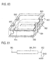
    4. The multilayer electronic part of claim 1 wherein said constituent layers include at least one first composite dielectric layer in which a dielectric powder having a dielectric constant of 5 to 10,000 and a dielectric dissipation factor of 0.00002 to 0.01 is dispersed in an amount of 10 to 65% by volume such that the first composite dielectric layer has a dielectric constant of 5 to 20 and a dielectric dissipation factor of 0.0025 to 0.0075.
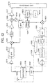
    5. The multilayer electronic part of claim 4 wherein said constituent layers include at least one second composite dielectric layer in which a dielectric powder having a dielectric constant of 20 to 20,000 and a dielectric dissipation factor of 0.01 to 0.0001 is dispersed in an amount of 10 to 65% by volume such that the second composite dielectric layer has a dielectric constant of 10 to 40 and a dielectric dissipation factor of 0.0075 to 0.025.
    6. The multilayer electronic part of claim 1 wherein said constituent layers include at least one composite magnetic layer in which a magnetic powder is dispersed in an amount of 10 to 65% by volume such that the composite magnetic layer has a magnetic permeability of 3 to 20.
    7. The multilayer electronic part of claim 1 wherein said constituent layers include at least one layer containing at least one flame retardant.
    EP00311741A 2000-05-31 2000-12-28 Electronic parts Withdrawn EP1160972A3 (en)

    Applications Claiming Priority (2)

    Application Number Priority Date Filing Date Title
    JP2000163418 2000-05-31
    JP2000163418A JP2001345212A (en) 2000-05-31 2000-05-31 Laminated electronic part

    Publications (2)

    Publication Number Publication Date
    EP1160972A2 true EP1160972A2 (en) 2001-12-05
    EP1160972A3 EP1160972A3 (en) 2003-09-17

    Family

    ID=18667171

    Family Applications (1)

    Application Number Title Priority Date Filing Date
    EP00311741A Withdrawn EP1160972A3 (en) 2000-05-31 2000-12-28 Electronic parts

    Country Status (4)

    Country Link
    US (1) US6713162B2 (en)
    EP (1) EP1160972A3 (en)
    JP (1) JP2001345212A (en)
    KR (1) KR100500150B1 (en)

    Cited By (8)

    * Cited by examiner, † Cited by third party
    Publication number Priority date Publication date Assignee Title
    WO2002063324A3 (en) * 2001-02-07 2002-10-24 Forschungszentrum Juelich Gmbh Rf-squid magnetometer
    US7548135B2 (en) 2005-04-21 2009-06-16 Fujitsu Media Devices Filter and duplexer
    US7754970B2 (en) 2005-06-15 2010-07-13 Toyo Boseki Kabushiki Kaisha High frequency electronic part
    WO2011133268A1 (en) * 2010-04-23 2011-10-27 Cooper Technolgies Company Miniature power inductor and methods of manufacture
    CN101331651B (en) * 2006-04-14 2013-01-30 株式会社村田制作所 antenna
    WO2017200701A1 (en) * 2016-05-20 2017-11-23 Qualcomm Incorporated Double-sided circuit
    CN108258912A (en) * 2015-09-11 2018-07-06 万国半导体(开曼)股份有限公司 Pulse transformer
    CN114388244A (en) * 2020-10-22 2022-04-22 Tdk株式会社 Coil component

    Families Citing this family (118)

    * Cited by examiner, † Cited by third party
    Publication number Priority date Publication date Assignee Title
    US6896826B2 (en) * 1997-01-09 2005-05-24 Advanced Technology Materials, Inc. Aqueous cleaning composition containing copper-specific corrosion inhibitor for cleaning inorganic residues on semiconductor substrate
    US6908960B2 (en) * 1999-12-28 2005-06-21 Tdk Corporation Composite dielectric material, composite dielectric substrate, prepreg, coated metal foil, molded sheet, composite magnetic substrate, substrate, double side metal foil-clad substrate, flame retardant substrate, polyvinylbenzyl ether resin composition, thermosettin
    EP1231637A3 (en) * 2001-02-08 2004-08-25 Hitachi, Ltd. High dielectric constant composite material and multilayer wiring board using the same
    DE10122393A1 (en) * 2001-05-09 2002-11-14 Philips Corp Intellectual Pty Flexible conductor foil with an electronic circuit
    US6911889B2 (en) * 2001-08-20 2005-06-28 Steward, Inc. High frequency filter device and related methods
    US20030042044A1 (en) * 2001-08-30 2003-03-06 Micron Technology, Inc. Circuit board plane interleave apparatus and method
    JP2003332749A (en) * 2002-01-11 2003-11-21 Denso Corp Substrate with built-in passive element, method for manufacturing the same, and base plate for forming substrate with built-in passive element
    US6900708B2 (en) * 2002-06-26 2005-05-31 Georgia Tech Research Corporation Integrated passive devices fabricated utilizing multi-layer, organic laminates
    US6987307B2 (en) * 2002-06-26 2006-01-17 Georgia Tech Research Corporation Stand-alone organic-based passive devices
    US7260890B2 (en) * 2002-06-26 2007-08-28 Georgia Tech Research Corporation Methods for fabricating three-dimensional all organic interconnect structures
    KR20040001294A (en) * 2002-06-27 2004-01-07 (주) 래트론 Distributed constant type filter
    US7101813B2 (en) * 2002-12-04 2006-09-05 Micron Technology Inc. Atomic layer deposited Zr-Sn-Ti-O films
    EP1580235A4 (en) * 2002-12-27 2007-05-30 Tdk Corp RESIN COMPOSITION, CURED RESIN, CURED RESIN SHEET, LAMINATE, PREIMPREGNE, ELECTRONIC COMPONENT, AND MULTILAYER SUBSTRATE
    JP3827314B2 (en) * 2003-03-17 2006-09-27 Tdk株式会社 Inductive device manufacturing method
    US7471170B2 (en) * 2003-03-21 2008-12-30 Nxp B.V. Multilayer stack with compensated resonant circuit
    US7489914B2 (en) * 2003-03-28 2009-02-10 Georgia Tech Research Corporation Multi-band RF transceiver with passive reuse in organic substrates
    TWI224798B (en) * 2003-04-04 2004-12-01 Via Tech Inc Transformer formed between two layout layers
    JP4493946B2 (en) * 2003-07-03 2010-06-30 財団法人国際科学振興財団 Chip element
    TWI227502B (en) 2003-09-02 2005-02-01 Ind Tech Res Inst Precise multi-pole magnetic components and manufacturing method thereof
    US8345433B2 (en) * 2004-07-08 2013-01-01 Avx Corporation Heterogeneous organic laminate stack ups for high frequency applications
    US7601649B2 (en) 2004-08-02 2009-10-13 Micron Technology, Inc. Zirconium-doped tantalum oxide films
    US7796401B2 (en) 2004-09-29 2010-09-14 Foundation For Advancement Of International Science Chip element
    KR100768919B1 (en) * 2004-12-23 2007-10-19 삼성전자주식회사 Power generating device
    WO2006073029A1 (en) * 2005-01-07 2006-07-13 Murata Manufacturing Co., Ltd. Electronic component and electronic component manufacturing method
    US7927948B2 (en) 2005-07-20 2011-04-19 Micron Technology, Inc. Devices with nanocrystals and methods of formation
    US20070140698A1 (en) * 2005-12-20 2007-06-21 Bookham Technology Plc Radio frequency signal device biasing circuit
    CN101253825A (en) * 2005-09-30 2008-08-27 松下电器产业株式会社 Chip composite electronic component and manufacturing method thereof
    WO2007049692A1 (en) * 2005-10-27 2007-05-03 Kabushiki Kaisha Toshiba Planar magnetic device and power supply ic package using same
    WO2007080680A1 (en) * 2006-01-16 2007-07-19 Murata Manufacturing Co., Ltd. Method for manufacturing inductor
    JP2007243531A (en) * 2006-03-08 2007-09-20 Matsushita Electric Ind Co Ltd LC filter
    US7875955B1 (en) 2006-03-09 2011-01-25 National Semiconductor Corporation On-chip power inductor
    JP2007267217A (en) * 2006-03-29 2007-10-11 Fujitsu Component Ltd Antenna device
    US9064198B2 (en) * 2006-04-26 2015-06-23 Murata Manufacturing Co., Ltd. Electromagnetic-coupling-module-attached article
    WO2007138800A1 (en) * 2006-06-01 2007-12-06 Murata Manufacturing Co., Ltd. Layered type balloon transformer
    US7750787B2 (en) * 2006-06-22 2010-07-06 Broadcom Corporation Impedance transformer and applications thereof
    US7439840B2 (en) 2006-06-27 2008-10-21 Jacket Micro Devices, Inc. Methods and apparatuses for high-performing multi-layer inductors
    US8232621B2 (en) * 2006-07-28 2012-07-31 Semiconductor Energy Laboratory Co., Ltd. Semiconductor device
    US7838976B2 (en) * 2006-07-28 2010-11-23 Semiconductor Energy Laboratory Co., Ltd. Semiconductor device having a semiconductor chip enclosed by a body structure and a base
    KR101478810B1 (en) 2006-07-28 2015-01-02 가부시키가이샤 한도오따이 에네루기 켄큐쇼 Power storage device
    US7808434B2 (en) * 2006-08-09 2010-10-05 Avx Corporation Systems and methods for integrated antennae structures in multilayer organic-based printed circuit devices
    US8466764B2 (en) * 2006-09-12 2013-06-18 Cooper Technologies Company Low profile layered coil and cores for magnetic components
    US9589716B2 (en) 2006-09-12 2017-03-07 Cooper Technologies Company Laminated magnetic component and manufacture with soft magnetic powder polymer composite sheets
    US8378777B2 (en) * 2008-07-29 2013-02-19 Cooper Technologies Company Magnetic electrical device
    US7791445B2 (en) * 2006-09-12 2010-09-07 Cooper Technologies Company Low profile layered coil and cores for magnetic components
    US8310332B2 (en) * 2008-10-08 2012-11-13 Cooper Technologies Company High current amorphous powder core inductor
    US7989895B2 (en) 2006-11-15 2011-08-02 Avx Corporation Integration using package stacking with multi-layer organic substrates
    JP4730313B2 (en) * 2007-01-24 2011-07-20 ミツミ電機株式会社 High frequency tuner module and tuner module
    EP2341463A3 (en) * 2007-04-19 2014-06-11 BALLUFF GmbH Data carrier/transmission device and method for manufacturing it
    US8063316B2 (en) * 2007-06-14 2011-11-22 Flextronics Ap Llc Split wave compensation for open stubs
    WO2009004605A2 (en) * 2007-07-05 2009-01-08 Origin Gps Ltd. Miniature patch antenna with increased gain
    TW200905703A (en) * 2007-07-27 2009-02-01 Delta Electronics Inc Magnetic device and manufacturing method thereof
    TWI402866B (en) * 2007-08-29 2013-07-21 Ind Tech Res Inst Suspension inductor devices
    TWI399139B (en) * 2007-09-19 2013-06-11 Ind Tech Res Inst Meander inductor and printed circuit board with a meander inductor
    JP2009088161A (en) * 2007-09-28 2009-04-23 Fujitsu Media Device Kk Electronic component
    US7463112B1 (en) 2007-11-30 2008-12-09 International Business Machines Corporation Area efficient, differential T-coil impedance-matching circuit for high speed communications applications
    JP4840381B2 (en) * 2008-03-07 2011-12-21 Tdk株式会社 Common mode filter and manufacturing method thereof
    TWI350655B (en) * 2008-03-20 2011-10-11 Ind Tech Res Inst Circuit device with inductor and capacitor in parallel connection
    CN101981635B (en) * 2008-04-08 2013-09-25 株式会社村田制作所 Electronic component
    US8279037B2 (en) * 2008-07-11 2012-10-02 Cooper Technologies Company Magnetic components and methods of manufacturing the same
    US8659379B2 (en) 2008-07-11 2014-02-25 Cooper Technologies Company Magnetic components and methods of manufacturing the same
    US9859043B2 (en) * 2008-07-11 2018-01-02 Cooper Technologies Company Magnetic components and methods of manufacturing the same
    US9558881B2 (en) 2008-07-11 2017-01-31 Cooper Technologies Company High current power inductor
    KR100992233B1 (en) * 2008-09-26 2010-11-05 삼성전기주식회사 Fabrication method of chip capacitor using ceramic / polymer composite
    FR2939990B1 (en) * 2008-12-11 2016-02-19 Commissariat Energie Atomique THIN FILM WITH HIGH PERMITTIVITY AND PERMEABILITY.
    DE102009012516B4 (en) * 2009-03-10 2011-02-10 Epcos Ag Multi-layer substrate for highly integrated module
    US20100277267A1 (en) * 2009-05-04 2010-11-04 Robert James Bogert Magnetic components and methods of manufacturing the same
    TW201121220A (en) * 2009-12-10 2011-06-16 Delta Electronics Inc DC-to-DC converting apparatus with communication function for vehicle
    US20110291788A1 (en) * 2010-05-26 2011-12-01 Tyco Electronics Corporation Planar inductor devices
    US8505192B2 (en) * 2010-10-08 2013-08-13 Advance Furnace Systems Corp. Manufacturing method of common mode filter
    US20120169444A1 (en) * 2010-12-30 2012-07-05 Samsung Electro-Mechanics Co., Ltd. Laminated inductor and method of manufacturing the same
    US20120229986A1 (en) * 2011-03-09 2012-09-13 Muzahid Bin Huda Power conversion system using ferromagnetic enclosure with embedded winding to serve as magnetic component
    JP5794218B2 (en) * 2012-02-14 2015-10-14 株式会社村田製作所 High frequency signal line and electronic device equipped with the same
    JP2014027094A (en) * 2012-07-26 2014-02-06 Dexerials Corp Coil module and power receiving device
    US10840005B2 (en) 2013-01-25 2020-11-17 Vishay Dale Electronics, Llc Low profile high current composite transformer
    US10070518B2 (en) 2013-02-06 2018-09-04 Isola Usa Corp. Prepregs and laminates having homogeneous dielectric properties
    US20150002256A1 (en) * 2013-03-11 2015-01-01 Bourns, Inc. Devices and methods related to laminated polymeric planar magnetics
    US9537205B2 (en) 2013-11-08 2017-01-03 Taiwan Semiconductor Manufacturing Company, Ltd. 3D antenna for integrated circuits
    US9496085B2 (en) 2014-01-03 2016-11-15 Hamilton Sundstrand Corporation Method of manufacturing an inductor coil
    KR20150090445A (en) 2014-01-29 2015-08-06 주식회사 이노칩테크놀로지 Laminated chip device
    KR102305618B1 (en) * 2014-10-02 2021-09-29 아이솔라 유에스에이 코프 Prepregs and laminates having homogeneous dielectric properties
    KR101642643B1 (en) * 2015-01-27 2016-07-29 삼성전기주식회사 Coil component and method of manufacturing the same
    KR20160114792A (en) * 2015-03-24 2016-10-06 삼성전기주식회사 Coil embeded integrated circuit substrate and manufacturing method thereof
    JP6540808B2 (en) * 2015-07-24 2019-07-10 株式会社村田製作所 Flexible inductor
    US9986651B2 (en) * 2015-10-30 2018-05-29 Dell Products, Lp Method for mitigating signal attenuation in printed circuit board connections
    KR101792365B1 (en) 2015-12-18 2017-11-01 삼성전기주식회사 Coil component and manufacturing method for the same
    US12058814B2 (en) 2016-03-03 2024-08-06 Delta Electronics (Shanghai) Co., Ltd. Power module and manufacturing method thereof
    US11277067B2 (en) 2016-03-03 2022-03-15 Delta Electronics, Inc. Power module and manufacturing method thereof
    CN107154301B (en) * 2016-03-03 2018-12-25 台达电子企业管理(上海)有限公司 magnetic assembly
    KR101883046B1 (en) * 2016-04-15 2018-08-24 삼성전기주식회사 Coil Electronic Component
    US10998124B2 (en) 2016-05-06 2021-05-04 Vishay Dale Electronics, Llc Nested flat wound coils forming windings for transformers and inductors
    CN109644566B (en) * 2016-08-15 2023-08-08 株式会社力森诺科 Adhesive films for multilayer printed wiring boards
    KR102571361B1 (en) 2016-08-31 2023-08-25 비쉐이 데일 일렉트로닉스, 엘엘씨 Inductor having high current coil with low direct current resistance
    JP6520875B2 (en) * 2016-09-12 2019-05-29 株式会社村田製作所 Inductor component and inductor component built-in substrate
    JP6594837B2 (en) * 2016-09-30 2019-10-23 太陽誘電株式会社 Coil parts
    US10566129B2 (en) 2016-09-30 2020-02-18 Taiyo Yuden Co., Ltd. Electronic component
    JP6752764B2 (en) * 2016-09-30 2020-09-09 太陽誘電株式会社 Coil parts
    KR102364013B1 (en) * 2016-12-07 2022-02-16 웨이퍼 엘엘씨 Low-loss electric transmission mechanism and antenna using the same
    CN108288532B (en) * 2017-01-09 2021-04-27 三星电机株式会社 Common Mode Filter
    KR20180092510A (en) * 2017-02-09 2018-08-20 삼성전기주식회사 Common mode filter
    JP6766702B2 (en) * 2017-03-09 2020-10-14 Tdk株式会社 Dielectric element
    WO2018178772A2 (en) * 2017-03-28 2018-10-04 Nanofone Ltd. High performance sealed-gap capacitive microphone
    KR101942732B1 (en) * 2017-04-12 2019-01-28 삼성전기 주식회사 Inductor and manufacturing method of the same
    JP6946721B2 (en) 2017-05-03 2021-10-06 Tdk株式会社 Coil parts
    TWI706424B (en) * 2018-06-27 2020-10-01 合利億股份有限公司 Wireless charging coil
    US11277917B2 (en) 2019-03-12 2022-03-15 Advanced Semiconductor Engineering, Inc. Embedded component package structure, embedded type panel substrate and manufacturing method thereof
    US11296030B2 (en) 2019-04-29 2022-04-05 Advanced Semiconductor Engineering, Inc. Embedded component package structure and manufacturing method thereof
    US10950551B2 (en) 2019-04-29 2021-03-16 Advanced Semiconductor Engineering, Inc. Embedded component package structure and manufacturing method thereof
    KR102406974B1 (en) * 2019-06-04 2022-06-10 한국전자기술연구원 Multilayer Chip Inductor with Magnetic/Dielectric Composite Structure
    KR20210012247A (en) * 2019-07-24 2021-02-03 주식회사 모다이노칩 Chip element
    JP7428960B2 (en) * 2019-10-08 2024-02-07 Tdk株式会社 Laminated electronic components and their manufacturing method
    US12567533B2 (en) 2020-03-03 2026-03-03 Vishay Dale Electronics, Llc Inductor with preformed termination and method and assembly for making the same
    WO2022020984A1 (en) * 2020-07-27 2022-02-03 华为技术有限公司 Inductive device and electronic apparatus
    KR102887275B1 (en) * 2020-11-11 2025-11-17 엘지이노텍 주식회사 Phase shifter
    WO2022123792A1 (en) * 2020-12-11 2022-06-16 昭和電工マテリアルズ株式会社 Resin composition for molding and electronic component device
    USD1034462S1 (en) 2021-03-01 2024-07-09 Vishay Dale Electronics, Llc Inductor package
    US11948724B2 (en) 2021-06-18 2024-04-02 Vishay Dale Electronics, Llc Method for making a multi-thickness electro-magnetic device
    JP2023012187A (en) * 2021-07-13 2023-01-25 株式会社村田製作所 Inductor component and mounting structure for inductor component
    JP7829317B2 (en) * 2021-12-28 2026-03-13 Tdk株式会社 Laminated coil components

    Family Cites Families (15)

    * Cited by examiner, † Cited by third party
    Publication number Priority date Publication date Assignee Title
    JP2610487B2 (en) * 1988-06-10 1997-05-14 株式会社日立製作所 Ceramic laminated circuit board
    JPH0548271A (en) * 1991-08-12 1993-02-26 Murata Mfg Co Ltd Functional multilayer circuit board
    EP0616221B1 (en) * 1993-03-19 1998-11-25 Murata Manufacturing Co., Ltd. Acceleration sensor
    JP2818926B2 (en) * 1994-11-16 1998-10-30 大塚化学株式会社 Resin composition for high frequency electronic components
    JP3511110B2 (en) * 1995-02-13 2004-03-29 日立化成工業株式会社 High dielectric constant and low dielectric loss tangent laminate
    JP3103296B2 (en) * 1995-06-30 2000-10-30 ティーディーケイ株式会社 Dielectric porcelain, method of manufacturing the same, and electronic component using the same
    JP3501327B2 (en) 1995-12-28 2004-03-02 株式会社村田製作所 LC resonance components
    CN1160854C (en) 1996-06-10 2004-08-04 富士电机株式会社 Noise Suppression Filters for Power Converters
    JP3438859B2 (en) * 1996-11-21 2003-08-18 ティーディーケイ株式会社 Laminated electronic component and manufacturing method thereof
    JP3610191B2 (en) * 1997-06-03 2005-01-12 Tdk株式会社 Non-magnetic ceramic and ceramic laminated parts
    DE19733104A1 (en) * 1997-07-31 1999-02-04 Wacker Chemie Gmbh Crosslinkable powder composition redispersible in water
    JPH11154805A (en) * 1997-09-22 1999-06-08 Tdk Corp Laminated ceramic part
    JPH11228222A (en) * 1997-12-11 1999-08-24 Murata Mfg Co Ltd Dielectric ceramic composition and ceramic electronic part using the same
    JPH11317311A (en) * 1998-03-03 1999-11-16 Matsushita Electric Ind Co Ltd Composite part and method of manufacturing the same
    US6239715B1 (en) * 1999-07-21 2001-05-29 Karen L. Belton Beeper system

    Cited By (10)

    * Cited by examiner, † Cited by third party
    Publication number Priority date Publication date Assignee Title
    WO2002063324A3 (en) * 2001-02-07 2002-10-24 Forschungszentrum Juelich Gmbh Rf-squid magnetometer
    US7548135B2 (en) 2005-04-21 2009-06-16 Fujitsu Media Devices Filter and duplexer
    US7754970B2 (en) 2005-06-15 2010-07-13 Toyo Boseki Kabushiki Kaisha High frequency electronic part
    CN101331651B (en) * 2006-04-14 2013-01-30 株式会社村田制作所 antenna
    WO2011133268A1 (en) * 2010-04-23 2011-10-27 Cooper Technolgies Company Miniature power inductor and methods of manufacture
    CN108258912A (en) * 2015-09-11 2018-07-06 万国半导体(开曼)股份有限公司 Pulse transformer
    CN108258912B (en) * 2015-09-11 2020-04-28 万国半导体(开曼)股份有限公司 Pulse transformer
    WO2017200701A1 (en) * 2016-05-20 2017-11-23 Qualcomm Incorporated Double-sided circuit
    US10103703B2 (en) 2016-05-20 2018-10-16 Qualcomm Incorporated Double-sided circuit
    CN114388244A (en) * 2020-10-22 2022-04-22 Tdk株式会社 Coil component

    Also Published As

    Publication number Publication date
    JP2001345212A (en) 2001-12-14
    EP1160972A3 (en) 2003-09-17
    KR20010109462A (en) 2001-12-10
    US20020009577A1 (en) 2002-01-24
    KR100500150B1 (en) 2005-07-11
    US6713162B2 (en) 2004-03-30

    Similar Documents

    Publication Publication Date Title
    US6713162B2 (en) Electronic parts
    EP1260998A1 (en) Electronic component-use substrate and electronic component
    US7060350B2 (en) Composite magnetic material and magnetic molding material, magnetic powder compression molding material, and magnetic paint using the composite magnetic material, composite dielectric material and molding material, powder compression molding material, paint, prepreg, and substrate using the composite dielectric material, and electronic part
    US6808642B2 (en) Method for producing multilayer substrate and electronic part, and multilayer electronic part
    US6908960B2 (en) Composite dielectric material, composite dielectric substrate, prepreg, coated metal foil, molded sheet, composite magnetic substrate, substrate, double side metal foil-clad substrate, flame retardant substrate, polyvinylbenzyl ether resin composition, thermosettin
    JP2001338813A (en) Electronic part
    JP2003297634A (en) Electronic component
    JP2003273520A (en) Stacked module
    JP3546001B2 (en) Electronic components
    JP2004363553A (en) Substrate, laminated electronic component and substrate manufacturing method
    JP2004221603A (en) Coupler
    JP2002305366A (en) Manufacturing method of laminated board and electronic component
    JP2003318029A (en) Laminated electronic component
    JP2004111908A (en) High-frequency electronic component
    JP2004201333A (en) Balun transformer
    JP2004207747A (en) Capacitor
    JP2004158879A (en) Inductor
    JP2003309425A (en) Patch antenna
    JP2004006897A (en) Multilayer electronic component
    JP2004096713A (en) Antenna
    JP2003289007A (en) Electronic component
    JP2003283221A (en) Electronic component
    JP2004207746A (en) Module
    JP2004208324A (en) Filter
    JP2004173308A (en) Antenna

    Legal Events

    Date Code Title Description
    PUAI Public reference made under article 153(3) epc to a published international application that has entered the european phase

    Free format text: ORIGINAL CODE: 0009012

    AK Designated contracting states

    Kind code of ref document: A2

    Designated state(s): AT BE CH CY DE DK ES FI FR GB GR IE IT LI LU MC NL PT SE TR

    AX Request for extension of the european patent

    Free format text: AL;LT;LV;MK;RO;SI

    PUAL Search report despatched

    Free format text: ORIGINAL CODE: 0009013

    AK Designated contracting states

    Kind code of ref document: A3

    Designated state(s): AT BE CH CY DE DK ES FI FR GB GR IE IT LI LU MC NL PT SE TR

    AX Request for extension of the european patent

    Extension state: AL LT LV MK RO SI

    17P Request for examination filed

    Effective date: 20031202

    AKX Designation fees paid

    Designated state(s): DE FI FR GB NL

    17Q First examination report despatched

    Effective date: 20060822

    STAA Information on the status of an ep patent application or granted ep patent

    Free format text: STATUS: THE APPLICATION IS DEEMED TO BE WITHDRAWN

    18D Application deemed to be withdrawn

    Effective date: 20070103