EP1151338B1 - Optischer steckverbinder - Google Patents
Optischer steckverbinder Download PDFInfo
- Publication number
- EP1151338B1 EP1151338B1 EP99902486A EP99902486A EP1151338B1 EP 1151338 B1 EP1151338 B1 EP 1151338B1 EP 99902486 A EP99902486 A EP 99902486A EP 99902486 A EP99902486 A EP 99902486A EP 1151338 B1 EP1151338 B1 EP 1151338B1
- Authority
- EP
- European Patent Office
- Prior art keywords
- plug
- socket
- locking
- outer housing
- locking means
- Prior art date
- Legal status (The legal status is an assumption and is not a legal conclusion. Google has not performed a legal analysis and makes no representation as to the accuracy of the status listed.)
- Expired - Lifetime
Links
- 230000003287 optical effect Effects 0.000 title claims abstract description 18
- 238000003780 insertion Methods 0.000 claims abstract description 35
- 230000037431 insertion Effects 0.000 claims abstract description 35
- 239000000835 fiber Substances 0.000 claims description 20
- 210000005069 ears Anatomy 0.000 claims description 5
- 230000000694 effects Effects 0.000 claims description 4
- 238000006073 displacement reaction Methods 0.000 claims description 3
- 238000010276 construction Methods 0.000 abstract 1
- 230000007246 mechanism Effects 0.000 description 13
- 238000000034 method Methods 0.000 description 7
- 239000013307 optical fiber Substances 0.000 description 7
- 230000008569 process Effects 0.000 description 7
- 239000000243 solution Substances 0.000 description 3
- 230000008901 benefit Effects 0.000 description 2
- 238000005516 engineering process Methods 0.000 description 2
- 230000003993 interaction Effects 0.000 description 2
- 230000001681 protective effect Effects 0.000 description 2
- 210000002023 somite Anatomy 0.000 description 2
- 230000015572 biosynthetic process Effects 0.000 description 1
- 230000008859 change Effects 0.000 description 1
- 238000011109 contamination Methods 0.000 description 1
- 230000001419 dependent effect Effects 0.000 description 1
- 239000000428 dust Substances 0.000 description 1
- 238000001746 injection moulding Methods 0.000 description 1
- 239000002655 kraft paper Substances 0.000 description 1
- 238000004519 manufacturing process Methods 0.000 description 1
- 230000005855 radiation Effects 0.000 description 1
- 230000000630 rising effect Effects 0.000 description 1
- 230000001360 synchronised effect Effects 0.000 description 1
Images



Classifications
-
- G—PHYSICS
- G02—OPTICS
- G02B—OPTICAL ELEMENTS, SYSTEMS OR APPARATUS
- G02B6/00—Light guides; Structural details of arrangements comprising light guides and other optical elements, e.g. couplings
- G02B6/24—Coupling light guides
- G02B6/36—Mechanical coupling means
- G02B6/38—Mechanical coupling means having fibre to fibre mating means
- G02B6/3807—Dismountable connectors, i.e. comprising plugs
- G02B6/389—Dismountable connectors, i.e. comprising plugs characterised by the method of fastening connecting plugs and sockets, e.g. screw- or nut-lock, snap-in, bayonet type
- G02B6/3893—Push-pull type, e.g. snap-in, push-on
-
- G—PHYSICS
- G02—OPTICS
- G02B—OPTICAL ELEMENTS, SYSTEMS OR APPARATUS
- G02B6/00—Light guides; Structural details of arrangements comprising light guides and other optical elements, e.g. couplings
- G02B6/24—Coupling light guides
- G02B6/36—Mechanical coupling means
- G02B6/38—Mechanical coupling means having fibre to fibre mating means
- G02B6/3807—Dismountable connectors, i.e. comprising plugs
- G02B6/3897—Connectors fixed to housings, casing, frames or circuit boards
-
- G—PHYSICS
- G02—OPTICS
- G02B—OPTICAL ELEMENTS, SYSTEMS OR APPARATUS
- G02B6/00—Light guides; Structural details of arrangements comprising light guides and other optical elements, e.g. couplings
- G02B6/24—Coupling light guides
- G02B6/42—Coupling light guides with opto-electronic elements
- G02B6/4296—Coupling light guides with opto-electronic elements coupling with sources of high radiant energy, e.g. high power lasers, high temperature light sources
- G02B2006/4297—Coupling light guides with opto-electronic elements coupling with sources of high radiant energy, e.g. high power lasers, high temperature light sources having protection means, e.g. protecting humans against accidental exposure to harmful laser radiation
-
- G—PHYSICS
- G02—OPTICS
- G02B—OPTICAL ELEMENTS, SYSTEMS OR APPARATUS
- G02B6/00—Light guides; Structural details of arrangements comprising light guides and other optical elements, e.g. couplings
- G02B6/24—Coupling light guides
- G02B6/36—Mechanical coupling means
- G02B6/38—Mechanical coupling means having fibre to fibre mating means
- G02B6/3807—Dismountable connectors, i.e. comprising plugs
- G02B6/3833—Details of mounting fibres in ferrules; Assembly methods; Manufacture
- G02B6/3847—Details of mounting fibres in ferrules; Assembly methods; Manufacture with means preventing fibre end damage, e.g. recessed fibre surfaces
- G02B6/3849—Details of mounting fibres in ferrules; Assembly methods; Manufacture with means preventing fibre end damage, e.g. recessed fibre surfaces using mechanical protective elements, e.g. caps, hoods, sealing membranes
Definitions
- the present invention relates to the field of optical fiber technology (LWL). It relates to an optical connector for releasable connection a circuit board with a backplane according to the preamble of claim 1.
- LWL optical fiber technology
- Such a connector is e.g. known from the document DE-C1-196 19 374.
- a second locking mechanism causes the plug when plugged into the Socket is locked with the inner housing and together with the inner Housing can move relative to the outer housing in the direction of insertion.
- the second locking mechanism is also on the side, but on the other Side of the connector, arranged. In this case the plug is firmly attached connected to the back wall, while the outer housing of the socket part is firmly mounted on the circuit board.
- the two locking mechanisms arranged on the side and acting independently of one another have several disadvantages: For the proper one When inserting it is important that the two locking mechanisms operated in a specific order (locked or unlocked) are, as this in FIGS. 3 (a) to 3 (j) of the publication mentioned is shown in detail. However, since the two locking mechanisms are arranged on opposite sides of the connector and independently function from each other, there is a risk that when plugging in by tilting the plug the correct order of operation is no longer guaranteed.
- the arrangement of the locking mechanisms on both sides is particularly unfavorable with regard to a flexible modular use of the connector with a freely selectable number of fiber optic individual connections, because one lateral expandability in a predetermined grid dimension is not possible.
- the releasable catches take place through an interaction between two spring arms (9) integrally formed on the plug-in part, the front ends of which are provided with bevels and locking shoulders, and two on one on the circuit board attached holding part molded (rigid) locking arms (28).
- Such a latching and unlocking mechanism requires a complicated sequence of movements when plugging in and accordingly a complex design the geometry and arrangement of the individual locking elements.
- the first locking means a Inner case attached first snap tab, which are in Plug direction extends and in the locked state behind one on the outer housing arranged first locking heel snaps
- the socket comprises an outer housing and an inner housing, which inner housing in the outer housing slidably mounted in the direction of insertion and by means of the first Locking means against displacement within the outer housing it is ensured that the at least one plug has a body with an insert part comprises that the second locking means one attached to the body include second snap tab, which extends in the direction of insertion and in the locked state behind one on the inner housing of the socket arranged second locking paragraph snaps, and that the two Snap tabs are designed and assigned to each other so that the second Snap tab when inserting the plug first behind the second locking shoulder snaps in and then the first snap over raises and unlocks the first locking heel.
- the solution according to the invention is characterized by simple structure and functional reliability and is inexpensive to manufacture using injection molding technology.
- the second locking means which are used for locking each other Plugs and sockets are provided for the unlocking of the first locking means used, which is the inner housing of the socket lock in the outer housing. This will force synchronization reached both unlocking and locking processes. Both are at the same time Locking mechanisms arranged compactly on the same side, so that the opposite side is freely available and is not subject to any restrictions. It goes without saying that there is no change in effect either the inner housing in the outer housing is displaceable at the socket can be formed, or the plug.
- the first and second locking means on the Circuit board facing or facing side of the connector are.
- the locking means attached very close to the longitudinal axis of the connector so that the contact pressure from the fiber optic ends that attack on the longitudinal axis result in only a small tilting moment, which none Wedging causes.
- a safe and low-friction interaction between the two snap tabs according to another preferred embodiment of the invention achieved in that the two snap tabs to each other at their free ends have parallel bevels that meet when they meet of the snap tabs when the plug is inserted a deflection of the effect the first snap tab transversely to the direction of insertion.
- To lock and unlock the second snap tab is at the level of second locking paragraph on the outer housing preferably a control track provided on which the second snap tab with its free end slides along when inserting and removing the plug and over the second locking paragraph is raised, for scanning the control path lateral ears are attached to the free end of the second snap tab.
- the connector 10 releasably connects four in the present example juxtaposed fiber optic cables 17 of a circuit board ("board") 14 with four corresponding optical cables 18, which run from a mounting rear wall (“backplane") 11 lead outwards.
- the circuit board 14 is oriented at right angles to the rear wall 11 of the assembly.
- the connector 10 comprises a connector 10A fixedly mounted on the edge of the circuit board 11 and a socket 10B matching the plug with an inner housing 13 which is slidably mounted in an outer housing 12 in the direction of insertion.
- the Outer housing 12 is in an opening in the opening by means of a flange 12A Mounting rear wall 11 attached (e.g. screwed).
- the connector 10A has a body 15, which - as can be seen from Fig. 2 - at one end in an insertion part 19 passes. With this insertion part 19, it is inserted into an insertion opening 22 (FIG. 2) the socket 10B.
- the connector 10A and the ends of the fiber optic therein Cable 17 can through a protective flap 16, the body 15th is pivotally mounted and pivoted back before insertion is protected against contamination or damage and against unintentional Leakage of radiation can be secured.
- FIG. 1 shows the connector 1 in a simplified, partially sectioned side view plugging together.
- the fiber optic cables and the details of the optical The connection between the cables is for reasons of clarity omitted.
- Locking means are provided on the side of the plug 10A for locking serve between the body 15 and the inner housing 13 and a Include snap tab 20.
- the snap tab 20 is at a distance below the insertion part 19 is arranged: It is preferably on the body 15 of the Molded connector 10A and extends in the direction of insertion, i.e., parallel to Plug-in part 19. It is the same length or a little shorter than the plug-in part 19, see above that they are largely protected from mechanical damage by the plug-in part 19 is protected. Due to its tongue-like configuration, the snap tab 20 can be elastically deflected transversely to the direction of insertion and can be hook-shaped free end behind a locking shoulder 24 provided for this purpose Snap into the inner housing 13 of the socket. The one necessary for locking Deflectability of the snap tab 20 downwards is ensured that the connector 10A with its body 15 so on the edge of the circuit board 14th is attached that insert 19 and snap tab 20 freely over the edge of the plate protrude.
- the snap tab 25 is on the underside of the inner housing 13 integrally formed and extends at a distance in the direction of insertion below the tapered front of the inner case 13.
- the locking heel 26, behind which the snap tab 25 with its hook-shaped free Can snap end is on the lower inner wall of the outer housing 12th formed.
- the distance of the snap tab 25 from the bottom of the inner housing 13 is chosen so that the tongue-shaped and transverse to Plug direction elastically deflectable snap tab 25 sufficiently far up can be deflected in order to get free from the locking shoulder 26 with the hook-shaped end.
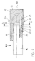
- the insertion process begins with a first phase in which the Plug 10A with the insertion part 19 in the insertion opening of the socket so far is introduced that the snap tab 20 with its hook-shaped end moved over the locking paragraph 24.
- the snap tab 20 is thereby deflected downwards so far that snap tab 20 and locking shoulder 24 practically do not touch.
- This is achieved through one or more appropriately shaped (trapezoidal) control tracks 23 on the outer housing 12 are formed at the level of the locking paragraph 24 and of the snap tab 20 with arranged at its hook-shaped end, laterally protruding ears 21 are scanned when inserted.
- the snap tab 20 returns on the rising slope of the control track 23 due to the elastic restoring forces back to their rest position and snaps behind the locking heel 24 a.
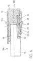
- the connector 10A and Bush 10B interlocked with each other, as well as the inner housing 13 and the outer housing 12; the connection between the optical fibers also works.
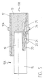
- the locking shoulders 24 and 26 and the two snap tabs 20 and 25 are shaped and arranged in relation to one another, that immediately after snapping the snap tab 20 behind the locking paragraph 24 this snap tab with its end face on the Face of the other snap tab 25 hits. Since the two snap tabs 20, 25 bevels running parallel to each other at their free ends (end faces) 27, 28 (Fig.
- the compactness of the locking means of the solution according to the invention becomes 7, which is a cross section through the 4 in the plane A-A and two adjacent on both sides, immediately adjacent, identical connectors 10 'and 10 "shows. It can be seen immediately that the on the underside of the connector 10, 10 ' and 10 "arranged, functionally interacting locking mechanisms, of which in Fig. 7 only the plug-side snap tab 20 with the side Ears 21, the locking heel 24 and the control tracks 23 can be seen enable a very narrow and flat design of the connector.
- the Space to the side and above is free for the actual elements of the fiber optic ends and for other functions such as an opened dust cover.
- the lateral space is required in particular for the elements of the optical fiber ends, because as the number of fibers increases, as many elements as possible the circuit board should be integrated.
- the connectors (10, 10 'and 10 "in FIG. 7) can thus be done without intermediate spacing and without a great loss of space be strung together between the individual optical connections.
- the Baying is particularly important if next to the optical connectors electrical (NF or HF) connectors, e.g. according to the Metral system become.
- the width of the optical connector corresponds to the width of the smallest Module of electrical connectors. Through this module formation is one flexible arrangement of electrical (NF or HF) and optical connectors guaranteed.
- Another advantage is the placement of the locking means according to FIG. 7 in the vertical center plane directly below the longitudinal axis of the connector.
- the locking means are so very close to the longitudinal axis of the Plug or socket. This ensures that the elements of the fiber-optic cable's contact pressure (point of attack on the longitudinal axis) result in only a small tilting moment that no wedging during the plugging process causes.
Landscapes
- Physics & Mathematics (AREA)
- General Physics & Mathematics (AREA)
- Optics & Photonics (AREA)
- Mechanical Coupling Of Light Guides (AREA)
- Optical Couplings Of Light Guides (AREA)
- Details Of Connecting Devices For Male And Female Coupling (AREA)
Description
- Fig. 1
- in einer perspektivischen Ansicht ein bevorzugtes Ausführungsbeispiel eines optischen Steckverbinders nach der Erfindung zur Verbindung von vier faseroptischen Kabeln im eingesteckten Zustand;
- Fig. 2
- in einer teilweise geschnittenen, der grösseren Uebersichtlichkeit wegen vereinfachten Seitenansicht ein Steckverbinder gemäss Fig. 1 vor dem Zusammenstecken;
- Fig. 3
- den Steckverbinder aus Fig. 2 in einer ersten Einsteckphase, in welcher die steckerseitige Schnapplasche die Steuerbahn am Aussengehäuse der Buchse abtastet und angehoben wird,
- Fig. 4
- den Steckverbinder aus Fig. 2 in einer zweiten Einsteckphase, in welcher die steckerseitige Schnapplasche hinter dem Verriegelungsabsatz am Innengehäuse der Buchse einrastet und Buchse und Stecker miteinander verriegelt;
- Fig. 5
- den Steckverbinder aus Fig. 2 in einer dritten Einsteckphase, in welcher die steckerseitige Schnapplasche die buchsenseitige Schnapplasche aus der Einrastposition anhebt;
- Fig. 6
- den Steckverbinder aus Fig. 2 nach Beendigung des Einsteckvorgangs, wobei die Verriegelung zwischen Innengehäuse und Aussengehäuse aufgehoben ist, und
- Fig. 7
- den Querschnitt durch einen Steckverbinder gemäss Fig. 4 in der dort eingezeichneten Ebene A-A (durchgezogene Linien) sowie in einer platzsparenden Aneinanderreihung zwei benachbarte identische Steckverbinder (strichpunktierte Linien).
- Nur während dem Einstecken wird eine Kraft zwischen der Schaltungsplatte ("board") und der Montagerückwand ("backplane") benötigt. Nach dem Verriegeln der zweiten Verriegelungsmittel bzw. nach dem Entriegeln der ersten Verriegelungsmittel besteht nach dem Einstecken Kraftfreiheit. Dadurch wird eine Deformation der Schaltungsplatte und der Montagerückwand vermieden.
- Die flache Bauweise der Verriegelungsmittel ermöglicht, dass die Verriegelungsmittel nur einseitig, aber sehr nahe an der Längsachse des Steckers bzw. der Buchse angebracht werden können. Die von den Elementen der Lichtwellenleiterenden herrührenden Anpresskräfte (Angriffsort auf der Längsachse) ergeben somit ein nur kleines Kippmoment, das keine Verkeilung hervorruft.
- Die einseitige Anordnung der Verriegelungsmittel hält den Raum seitlich und oben frei für die eigentlichen Elemente der Lichtwellenleiterenden und für weitere Funktionen. Der seitlichen Raum wird für die Elemente der Lichtwellenleiterenden benötigt, da mit steigendem Bedarf der Faseranzahl möglichst viele Elemente entlang der Schaltungsplatte integriert werden sollen. Die Steckverbinder können somit ohne Zwischenabstand und ohne grossen Platzverlust zwischen den einzelnen optischen Verbindungen aneinandergereiht werden.
- Die Breite des optischen Steckverbinders entspricht der Breite des kleinsten Moduls der elektrischen Steckverbinder. Durch die gleiche Modularität zu den elektrischen (NF oder HF) Steckverbindern, wie z.B. Metral-Steckverbinder, können die optischen und elektrischen Steckverbinder beliebig und damit flexibel aneinandergereiht werden.
- Innerhalb dieses Systems können flexibel 1 bis beispielsweise 4 Faserverbindungen pro Steckverbinder aneinandergereiht werden
- Die minimale Anzahl der Schnapplaschen je Verriegelungsmittel hält die Ein- bzw. Aussteckkraft niedrig.
- 10,10',10"
- optischer Steckverbinder ("backplane connector")
- 10A
- Stecker
- 10B
- Buchse
- 11
- Montagerückwand ("backplane")
- 12
- Aussengehäuse (Buchse)
- 12A
- Flansch
- 13
- Innengehäuse (Buchse)
- 14
- Schaltungsplatte
- 15
- Körper (Stecker)
- 16
- Schutzklappe (Stecker)
- 17,18
- faseroptisches Kabel
- 19
- Einsteckteil
- 20,25
- Schnapplasche
- 21
- seitliches Ohr
- 22
- Einstecköffnung
- 23
- Steuerbahn
- 24,26
- Verriegelungsabsatz
- 27,28
- Anschrägung
Claims (8)
- Optischer Steckverbinder (10) zum lösbaren Verbinden einer Schaltungsplatte (14) mit einer Montagerückwand (11), welcher Steckverbinder (10) wenigstens einen Stecker (10A) und wenigstens eine Buchse (10B) umfasst, wobei die Buchse (10B) oder der Stecker (10A) ein Aussengehäuse (12) und ein Innengehäuse (13) umfasst, welches Innengehäuse (13) in dem Aussengehäuse (12) in Steckrichtung verschiebbar gelagert und mittels erster Verriegelungsmittel (25, 26) gegen ein Verschieben innerhalb des Aussengehäuses (12) gesichert ist, und wobei dem Stecker (10A) oder der Buchse (10B) Entriegelungsmittel (20) zugeordnet sind, welche beim vollständigen Einstecken des Steckers (10A) in die Buchse (10B) die ersten Verriegelungsmittel (25, 26) entriegeln, und wobei dem Stecker (10A) oder der Buchse (10B) zweite Verriegelungsmittel (20, 21, 23, 24) zugeordnet sind, welche beim vollständigen Einstecken des Steckers (10A) den Stecker (10A) und die Buchse (10B) untereinander verriegeln, wobei die zweiten Verriegelungsmittel (20, 21, 23, 24) so ausgebildet sind, dass sie zugleich als Entriegelungsmittel für die ersten Verriegelungsmittel (25, 26) dienen, und die ersten Verriegelungsmittel (25, 26) eine am Innengehäuse (13) angebrachte erste Schnapplasche (25) umfassen, welche sich in Steckrichtung erstreckt und im verriegelten Zustand hinter einen am Aussengehäuse (12) angeordneten ersten Verriegelungsabsatz (26) einschnappt, und die Buchse (10B) ein Aussengehäuse (12) und ein Innengehäuse (13) umfasst, welches Innengehäuse (13) in dem Aussengehäuse (12) in Steckrichtung verschiebbar gelagert und mittels der ersten Verriegelungsmittel (25, 26) gegen ein Verschieben innerhalb des Aussengehäuses (12) gesichert ist, dadurch gekennzeichnet, dass der wenigstens eine Stecker (10A) einen Körper (15) mit einem Einsteckteil (19) umfasst, dass die zweiten Verriegelungsmittel (20, 21, 23, 24) eine an dem Körper (15) angebrachte zweite Schnapplasche (20) umfassen, welche sich in Steckrichtung erstreckt und im verriegelten Zustand hinter einen am Innengehäuse (13) der Buchse (10B) angeordneten zweiten Verriegelungsabsatz (24) einschnappt, und dass die beiden Schnapplaschen (20, 25) so ausgebildet und einander zugeordnet sind, dass die zweite Schnapplasche (20) beim Einstecken des Steckers (10A) zunächst hinter dem zweiten Verriegelungsabsatz (24) einschnappt und anschliessend die erste Schnapplasche (25) über den ersten Verriegelungsabsatz (26) anhebt und entriegelt.
- Steckverbinder nach Anspruch 1, dadurch gekennzeichnet, dass die ersten und zweiten Verriegelungsmittel (25, 26 bzw. 20, 21, 23, 24) auf der der Schaltungsplatte (14) zu oder abgewandten Seite des Steckverbinders (10) angeordnet sind.
- Steckverbinder nach Anspruch 1, dadurch gekennzeichnet, dass die beiden Schnapplaschen (20, 25) an ihren freien Enden zueinander parallel verlaufende Anschrägungen (27, 28) aufweisen, welche beim Aufeinandertreffen der Schnapplaschen (20, 25) beim Einstecken des Steckers (10A) eine Auslenkung der ersten Schnapplasche (25) quer zur Steckrichtung bewirken.
- Steckverbinder nach einem der Ansprüche 1 bis 3, dadurch gekennzeichnet, dass zum Verriegeln und Entriegeln der zweiten Schnapplasche (20) auf der Höhe des zweiten Verriegelungsabsatzes (24) am Aussengehäuse (12) eine Steuerbahn (23) vorgesehen ist, auf welcher die zweite Schnapplasche (20) mit ihrem freien Ende beim Einstecken und Herausziehen des Steckers (10A) entlanggleitet und über den zweiten Verriegelungsabsatz (24) gehoben wird.
- Steckverbinder nach Anspruch 4, dadurch gekennzeichnet, dass zum Abtasten der Steuerbahn (23) am freien Ende der zweiten Schnapplasche (20) seitliche Ohren (21) angebracht sind.
- Steckverbinder nach einem der Ansprüche 1 bis 5, dadurch gekennzeichnet, dass innerhalb des Steckverbinders (10) eine Mehrzahl von faseroptischen Kabeln (17, 18) verbunden werden.
- Steckverbinder nach einem der Ansprüche 1 bis 6, dadurch gekennzeichnet, dass die Buchse (10B) für die Montage an einer Montagerückwand (11) und der Stecker (10A) für die Montage auf einer Schaltungsplatte (14) vorgesehen ist.
- Steckverbinder nach Anspruch 7, dadurch gekennzeichnet, dass das Aussengehäuse (12) mit einem Flansch (12A) zur Befestigung an der Montagerückwand (11) ausgestattet ist.
Applications Claiming Priority (1)
| Application Number | Priority Date | Filing Date | Title |
|---|---|---|---|
| PCT/CH1999/000064 WO2000048030A1 (de) | 1999-02-12 | 1999-02-12 | Optischer steckverbinder |
Publications (2)
| Publication Number | Publication Date |
|---|---|
| EP1151338A1 EP1151338A1 (de) | 2001-11-07 |
| EP1151338B1 true EP1151338B1 (de) | 2003-10-01 |
Family
ID=4551655
Family Applications (1)
| Application Number | Title | Priority Date | Filing Date |
|---|---|---|---|
| EP99902486A Expired - Lifetime EP1151338B1 (de) | 1999-02-12 | 1999-02-12 | Optischer steckverbinder |
Country Status (10)
| Country | Link |
|---|---|
| US (1) | US6464403B1 (de) |
| EP (1) | EP1151338B1 (de) |
| JP (1) | JP3518678B2 (de) |
| CN (1) | CN1142455C (de) |
| AT (1) | ATE251314T1 (de) |
| AU (1) | AU2261899A (de) |
| CA (1) | CA2362194A1 (de) |
| DE (1) | DE59907236D1 (de) |
| TW (1) | TW468073B (de) |
| WO (1) | WO2000048030A1 (de) |
Families Citing this family (32)
| Publication number | Priority date | Publication date | Assignee | Title |
|---|---|---|---|---|
| US6315590B1 (en) | 2000-04-03 | 2001-11-13 | Molex Incorporated | Floating panel mounted connector assembly |
| KR20020067928A (ko) * | 2000-11-10 | 2002-08-24 | 소니 가부시끼 가이샤 | 접속장치 |
| JP2003156660A (ja) * | 2001-11-20 | 2003-05-30 | Auto Network Gijutsu Kenkyusho:Kk | 光コネクタ装置 |
| JP4117476B2 (ja) | 2003-05-30 | 2008-07-16 | 日本電気株式会社 | 光モジュール、光モジュールとケージとの組立体、光モジュールとケージとのロック方法及びロック解除方法 |
| US7144268B2 (en) | 2003-08-19 | 2006-12-05 | Spacelabs Medical, Inc. | Latching medical patient parameter safety connector and method |
| KR100424781B1 (ko) * | 2003-09-01 | 2004-03-31 | 에스티에스반도체통신 주식회사 | 양방향단자 usb 플러그를 구비한 usb 저장장치 |
| JP4454300B2 (ja) * | 2003-12-15 | 2010-04-21 | 住友電装株式会社 | コネクタ |
| JP2005181959A (ja) * | 2003-12-22 | 2005-07-07 | Rohm & Haas Electronic Materials Llc | 光ファイバーをプリント配線板の埋め込み型導波路に連結する方法および構造体 |
| US7347634B2 (en) * | 2004-08-06 | 2008-03-25 | Finisar Corporation | Opto-electrical module for optical signals from at least two optical data channels for arranging on a main circuit board of a component assembly and opto-electrical component assembly |
| KR100703288B1 (ko) * | 2004-11-03 | 2007-04-03 | 삼성전자주식회사 | 플러그형 광송수신기 모듈의 체결 장치 |
| JP2009210669A (ja) * | 2008-03-03 | 2009-09-17 | Furukawa Electric Co Ltd:The | コネクタユニット |
| US8403570B2 (en) * | 2008-04-10 | 2013-03-26 | Amphenol Corporation | Plural fiber optic interconnect |
| US8435062B2 (en) * | 2008-10-15 | 2013-05-07 | Fci | Latch assembly for a connector |
| US8417071B2 (en) | 2010-05-24 | 2013-04-09 | Xyratex Technology Limited | Data storage system, a modular printed circuit board, a backplane and a backplane component |
| CN102346279B (zh) * | 2010-07-30 | 2015-03-11 | 株式会社藤仓 | 光连接器、连接器连接系统 |
| CN102565957B (zh) * | 2010-12-31 | 2014-03-26 | 深圳日海通讯技术股份有限公司 | 一种光纤连接器 |
| CN103135175B (zh) * | 2011-12-01 | 2015-04-22 | 沈阳兴华航空电器有限责任公司 | 一种光纤阵列连接器 |
| JP6027859B2 (ja) * | 2012-11-16 | 2016-11-16 | 矢崎総業株式会社 | ハウジング接続構造 |
| CN102967903A (zh) * | 2012-11-28 | 2013-03-13 | 江苏宇特光电科技股份有限公司 | 单芯光纤连动连接插头 |
| JP6079893B2 (ja) | 2013-09-27 | 2017-02-15 | 株式会社村田製作所 | ヘッドフォン |
| US9494744B2 (en) | 2014-11-10 | 2016-11-15 | Corning Optical Communications LLC | Fiber optic connector having a main connector body and a plurality of removable sub-connectors |
| US9985359B2 (en) * | 2016-03-11 | 2018-05-29 | The Siemon Company | Field terminable telecommunications connector |
| CN209028258U (zh) | 2016-03-17 | 2019-06-25 | 康宁光电通信有限责任公司 | 可调谐光纤连接器、连接器子组件、电缆组件和子组件 |
| US9853397B1 (en) * | 2016-09-16 | 2017-12-26 | Te Connectivity Corporation | Pluggable module having pull tether for latch release |
| CN108459377B (zh) * | 2017-02-20 | 2021-07-06 | 中兴通讯股份有限公司 | 一种光波导组件 |
| TWI617853B (zh) * | 2017-03-03 | 2018-03-11 | 英屬維京群島商祥茂光電科技股份有限公司 | 光收發器 |
| CN110568562B (zh) * | 2018-06-05 | 2024-11-22 | 罗森伯格(上海)通信技术有限公司 | 一种光纤连接器 |
| US11215769B2 (en) * | 2019-03-07 | 2022-01-04 | Mellanox Technologies, Ltd. | MPO locking |
| US11726269B2 (en) * | 2019-09-24 | 2023-08-15 | Senko Advanced Components, Inc. | Lockable MPO connector for securing within a port of an adapter having a unique removal key |
| WO2022133730A1 (zh) * | 2020-12-22 | 2022-06-30 | 华为技术有限公司 | 一种光纤接口、光模块和通讯设备 |
| CN115275713B (zh) * | 2022-09-28 | 2022-12-16 | 深圳市西点精工技术有限公司 | 一种高速背板连接器 |
| CN117908196B (zh) * | 2024-03-19 | 2024-05-17 | 深圳市东强精密科技有限公司 | 一种光纤连接器组件 |
Family Cites Families (4)
| Publication number | Priority date | Publication date | Assignee | Title |
|---|---|---|---|---|
| US5121454A (en) * | 1989-11-24 | 1992-06-09 | Nippon Telegraph And Telephone Corporation | Optical connector |
| US5673346A (en) | 1989-11-24 | 1997-09-30 | Nippon Telegraph And Telephone Corporation | Optical jack for plug-jack optical connector |
| DE29607793U1 (de) * | 1996-05-02 | 1997-09-04 | HARTING KGaA, 32339 Espelkamp | Steckverbindung |
| EP0805366A1 (de) | 1996-05-02 | 1997-11-05 | Harting KGaA | Steckverbindung |
-
1999
- 1999-02-12 CN CNB998154253A patent/CN1142455C/zh not_active Expired - Fee Related
- 1999-02-12 JP JP2000598885A patent/JP3518678B2/ja not_active Expired - Fee Related
- 1999-02-12 EP EP99902486A patent/EP1151338B1/de not_active Expired - Lifetime
- 1999-02-12 CA CA002362194A patent/CA2362194A1/en not_active Abandoned
- 1999-02-12 AU AU22618/99A patent/AU2261899A/en not_active Abandoned
- 1999-02-12 WO PCT/CH1999/000064 patent/WO2000048030A1/de not_active Ceased
- 1999-02-12 DE DE59907236T patent/DE59907236D1/de not_active Expired - Fee Related
- 1999-02-12 US US09/890,415 patent/US6464403B1/en not_active Expired - Fee Related
- 1999-02-12 AT AT99902486T patent/ATE251314T1/de not_active IP Right Cessation
-
2000
- 2000-01-04 TW TW089100129A patent/TW468073B/zh not_active IP Right Cessation
Also Published As
| Publication number | Publication date |
|---|---|
| CN1142455C (zh) | 2004-03-17 |
| WO2000048030A1 (de) | 2000-08-17 |
| CN1332857A (zh) | 2002-01-23 |
| CA2362194A1 (en) | 2000-08-17 |
| ATE251314T1 (de) | 2003-10-15 |
| TW468073B (en) | 2001-12-11 |
| AU2261899A (en) | 2000-08-29 |
| DE59907236D1 (de) | 2003-11-06 |
| US6464403B1 (en) | 2002-10-15 |
| JP2002536699A (ja) | 2002-10-29 |
| EP1151338A1 (de) | 2001-11-07 |
| JP3518678B2 (ja) | 2004-04-12 |
Similar Documents
| Publication | Publication Date | Title |
|---|---|---|
| EP1151338A1 (de) | Optischer steckverbinder | |
| DE69432625T2 (de) | Faseroptische verbindungsanordnung | |
| DE69922470T2 (de) | Faseroptische Verbindungseinheit | |
| DE60018511T2 (de) | Ver- und Entriegelungsmechanismus eines Kabelverbinders und Verfahren zum Ver- und Entriegeln | |
| DE60027611T2 (de) | Kabelverbinder mit gesteuerter Impedanz | |
| EP0805366A1 (de) | Steckverbindung | |
| EP2904982B1 (de) | Elektrochirurgisches Gerät mit einem Buchseneinsatz, Set mit einem Entnahmewerkzeug und Verfahren zum entnehmen eines Buchseneinsatzes | |
| EP0991969B1 (de) | Ferrulencontainer und verbindungsanordnung für eine optische mehrfachfaser | |
| DE69705658T2 (de) | Modularer Aufbau, bestehend aus mehreren Einheiten, mit den entsprechenden Steckverbindern | |
| DE69027345T2 (de) | Verstärkte Verbinderverriegelung | |
| DE2807366A1 (de) | Verbinderanordnung | |
| DE102006012730B3 (de) | Befestigungssystem zum Befestigen eines Kabinenausstattungselements an einer Trägerstruktur eines Flugzeugs | |
| DE102017128604A1 (de) | Elektrische Steckverbindung zur Datenübertragung | |
| DE19642578C2 (de) | Steckverbinder mit einem Eingriffsbestätigungsmechanismus | |
| DE102021127033B3 (de) | Steckverbinderanordnung zum verbinden von signalleitern | |
| WO2021254822A1 (de) | Modular aufbaubaren steckverbinder | |
| DE102011002135A1 (de) | Steckerelement mit zweiter Kontaktsicherung | |
| EP4216377A1 (de) | Steckverbinder | |
| EP3440745B1 (de) | Wabenbaustein zur ausbildung einer rangierwabe, rangierwabe und werkzeug zum lösen eines wabenbausteins aus einer rangierwabe | |
| DE102020001995A1 (de) | Steckverbinderbaugruppe, Stecksystem und Verfahren | |
| DE19619374C1 (de) | Steckverbindung | |
| DE102016108780A1 (de) | Mittel zum Montieren, Entriegeln und Demontieren eines Steckverbinders, sowie Verfahren zur Nutzung des Mittels | |
| DE69809771T2 (de) | Schwimmende verbinderanordnung | |
| EP0746059B1 (de) | Elektrischer Steckverbinder | |
| DE102005050778B4 (de) | Kontaktgehäuse sowie elektrische Kontaktvorrichtung |
Legal Events
| Date | Code | Title | Description |
|---|---|---|---|
| PUAI | Public reference made under article 153(3) epc to a published international application that has entered the european phase |
Free format text: ORIGINAL CODE: 0009012 |
|
| 17P | Request for examination filed |
Effective date: 20010530 |
|
| AK | Designated contracting states |
Kind code of ref document: A1 Designated state(s): AT BE CH CY DE DK ES FI FR GB GR IE IT LI LU MC NL PT SE |
|
| GRAH | Despatch of communication of intention to grant a patent |
Free format text: ORIGINAL CODE: EPIDOS IGRA |
|
| GRAH | Despatch of communication of intention to grant a patent |
Free format text: ORIGINAL CODE: EPIDOS IGRA |
|
| GRAA | (expected) grant |
Free format text: ORIGINAL CODE: 0009210 |
|
| AK | Designated contracting states |
Kind code of ref document: B1 Designated state(s): AT BE CH CY DE DK ES FI FR GB GR IE IT LI LU MC NL PT SE |
|
| PG25 | Lapsed in a contracting state [announced via postgrant information from national office to epo] |
Ref country code: IE Free format text: LAPSE BECAUSE OF FAILURE TO SUBMIT A TRANSLATION OF THE DESCRIPTION OR TO PAY THE FEE WITHIN THE PRESCRIBED TIME-LIMIT Effective date: 20031001 Ref country code: FI Free format text: LAPSE BECAUSE OF FAILURE TO SUBMIT A TRANSLATION OF THE DESCRIPTION OR TO PAY THE FEE WITHIN THE PRESCRIBED TIME-LIMIT Effective date: 20031001 Ref country code: CY Free format text: LAPSE BECAUSE OF FAILURE TO SUBMIT A TRANSLATION OF THE DESCRIPTION OR TO PAY THE FEE WITHIN THE PRESCRIBED TIME-LIMIT Effective date: 20031001 |
|
| REG | Reference to a national code |
Ref country code: GB Ref legal event code: FG4D Free format text: NOT ENGLISH |
|
| REG | Reference to a national code |
Ref country code: CH Ref legal event code: EP |
|
| GBT | Gb: translation of ep patent filed (gb section 77(6)(a)/1977) | ||
| REG | Reference to a national code |
Ref country code: IE Ref legal event code: FG4D Free format text: GERMAN |
|
| REG | Reference to a national code |
Ref country code: CH Ref legal event code: NV Representative=s name: ISLER & PEDRAZZINI AG |
|
| REF | Corresponds to: |
Ref document number: 59907236 Country of ref document: DE Date of ref document: 20031106 Kind code of ref document: P |
|
| PG25 | Lapsed in a contracting state [announced via postgrant information from national office to epo] |
Ref country code: SE Free format text: LAPSE BECAUSE OF FAILURE TO SUBMIT A TRANSLATION OF THE DESCRIPTION OR TO PAY THE FEE WITHIN THE PRESCRIBED TIME-LIMIT Effective date: 20040101 Ref country code: GR Free format text: LAPSE BECAUSE OF FAILURE TO SUBMIT A TRANSLATION OF THE DESCRIPTION OR TO PAY THE FEE WITHIN THE PRESCRIBED TIME-LIMIT Effective date: 20040101 Ref country code: DK Free format text: LAPSE BECAUSE OF FAILURE TO SUBMIT A TRANSLATION OF THE DESCRIPTION OR TO PAY THE FEE WITHIN THE PRESCRIBED TIME-LIMIT Effective date: 20040101 |
|
| PG25 | Lapsed in a contracting state [announced via postgrant information from national office to epo] |
Ref country code: ES Free format text: LAPSE BECAUSE OF FAILURE TO SUBMIT A TRANSLATION OF THE DESCRIPTION OR TO PAY THE FEE WITHIN THE PRESCRIBED TIME-LIMIT Effective date: 20040112 |
|
| PGFP | Annual fee paid to national office [announced via postgrant information from national office to epo] |
Ref country code: CH Payment date: 20040127 Year of fee payment: 6 |
|
| PG25 | Lapsed in a contracting state [announced via postgrant information from national office to epo] |
Ref country code: LU Free format text: LAPSE BECAUSE OF NON-PAYMENT OF DUE FEES Effective date: 20040212 Ref country code: AT Free format text: LAPSE BECAUSE OF NON-PAYMENT OF DUE FEES Effective date: 20040212 |
|
| PGFP | Annual fee paid to national office [announced via postgrant information from national office to epo] |
Ref country code: NL Payment date: 20040217 Year of fee payment: 6 |
|
| PG25 | Lapsed in a contracting state [announced via postgrant information from national office to epo] |
Ref country code: MC Free format text: LAPSE BECAUSE OF NON-PAYMENT OF DUE FEES Effective date: 20040228 Ref country code: BE Free format text: LAPSE BECAUSE OF NON-PAYMENT OF DUE FEES Effective date: 20040228 |
|
| ET | Fr: translation filed | ||
| REG | Reference to a national code |
Ref country code: IE Ref legal event code: FD4D |
|
| PLBE | No opposition filed within time limit |
Free format text: ORIGINAL CODE: 0009261 |
|
| STAA | Information on the status of an ep patent application or granted ep patent |
Free format text: STATUS: NO OPPOSITION FILED WITHIN TIME LIMIT |
|
| BERE | Be: lapsed |
Owner name: *HUBER & SUHNER A.G. Effective date: 20040228 |
|
| 26N | No opposition filed |
Effective date: 20040702 |
|
| PG25 | Lapsed in a contracting state [announced via postgrant information from national office to epo] |
Ref country code: LI Free format text: LAPSE BECAUSE OF NON-PAYMENT OF DUE FEES Effective date: 20050228 Ref country code: CH Free format text: LAPSE BECAUSE OF NON-PAYMENT OF DUE FEES Effective date: 20050228 |
|
| PG25 | Lapsed in a contracting state [announced via postgrant information from national office to epo] |
Ref country code: NL Free format text: LAPSE BECAUSE OF NON-PAYMENT OF DUE FEES Effective date: 20050901 |
|
| REG | Reference to a national code |
Ref country code: CH Ref legal event code: PL |
|
| NLV4 | Nl: lapsed or anulled due to non-payment of the annual fee |
Effective date: 20050901 |
|
| PG25 | Lapsed in a contracting state [announced via postgrant information from national office to epo] |
Ref country code: PT Free format text: LAPSE BECAUSE OF NON-PAYMENT OF DUE FEES Effective date: 20040301 |
|
| PGFP | Annual fee paid to national office [announced via postgrant information from national office to epo] |
Ref country code: IT Payment date: 20080122 Year of fee payment: 10 Ref country code: GB Payment date: 20080118 Year of fee payment: 10 Ref country code: DE Payment date: 20080118 Year of fee payment: 10 |
|
| PGFP | Annual fee paid to national office [announced via postgrant information from national office to epo] |
Ref country code: FR Payment date: 20080114 Year of fee payment: 10 |
|
| GBPC | Gb: european patent ceased through non-payment of renewal fee |
Effective date: 20090212 |
|
| REG | Reference to a national code |
Ref country code: FR Ref legal event code: ST Effective date: 20091030 |
|
| PG25 | Lapsed in a contracting state [announced via postgrant information from national office to epo] |
Ref country code: DE Free format text: LAPSE BECAUSE OF NON-PAYMENT OF DUE FEES Effective date: 20090901 |
|
| PG25 | Lapsed in a contracting state [announced via postgrant information from national office to epo] |
Ref country code: GB Free format text: LAPSE BECAUSE OF NON-PAYMENT OF DUE FEES Effective date: 20090212 Ref country code: FR Free format text: LAPSE BECAUSE OF NON-PAYMENT OF DUE FEES Effective date: 20090302 |
|
| PG25 | Lapsed in a contracting state [announced via postgrant information from national office to epo] |
Ref country code: IT Free format text: LAPSE BECAUSE OF NON-PAYMENT OF DUE FEES Effective date: 20090212 |