EP1148404A1 - Régulateur de tension à faible consommation électrique - Google Patents
Régulateur de tension à faible consommation électrique Download PDFInfo
- Publication number
- EP1148404A1 EP1148404A1 EP01108243A EP01108243A EP1148404A1 EP 1148404 A1 EP1148404 A1 EP 1148404A1 EP 01108243 A EP01108243 A EP 01108243A EP 01108243 A EP01108243 A EP 01108243A EP 1148404 A1 EP1148404 A1 EP 1148404A1
- Authority
- EP
- European Patent Office
- Prior art keywords
- voltage
- amplifier
- regulator
- transistor
- regulation
- Prior art date
- Legal status (The legal status is an assumption and is not a legal conclusion. Google has not performed a legal analysis and makes no representation as to the accuracy of the status listed.)
- Granted
Links
- 230000001105 regulatory effect Effects 0.000 claims abstract description 22
- 230000033228 biological regulation Effects 0.000 claims description 36
- 238000000034 method Methods 0.000 claims description 10
- 230000010287 polarization Effects 0.000 claims description 3
- 238000012544 monitoring process Methods 0.000 claims 1
- 230000007423 decrease Effects 0.000 description 4
- 238000010586 diagram Methods 0.000 description 4
- 230000000903 blocking effect Effects 0.000 description 2
- 230000004913 activation Effects 0.000 description 1
- 239000003990 capacitor Substances 0.000 description 1
- 238000007599 discharging Methods 0.000 description 1
- 238000001914 filtration Methods 0.000 description 1
- 238000004519 manufacturing process Methods 0.000 description 1
- 244000045947 parasite Species 0.000 description 1
- 230000001172 regenerating effect Effects 0.000 description 1
- 239000011435 rock Substances 0.000 description 1
- 230000006641 stabilisation Effects 0.000 description 1
- 238000011105 stabilization Methods 0.000 description 1
- 230000000087 stabilizing effect Effects 0.000 description 1
- 230000007704 transition Effects 0.000 description 1
Images



Classifications
-
- G—PHYSICS
- G05—CONTROLLING; REGULATING
- G05F—SYSTEMS FOR REGULATING ELECTRIC OR MAGNETIC VARIABLES
- G05F1/00—Automatic systems in which deviations of an electric quantity from one or more predetermined values are detected at the output of the system and fed back to a device within the system to restore the detected quantity to its predetermined value or values, i.e. retroactive systems
- G05F1/10—Regulating voltage or current
- G05F1/46—Regulating voltage or current wherein the variable actually regulated by the final control device is DC
- G05F1/56—Regulating voltage or current wherein the variable actually regulated by the final control device is DC using semiconductor devices in series with the load as final control devices
- G05F1/565—Regulating voltage or current wherein the variable actually regulated by the final control device is DC using semiconductor devices in series with the load as final control devices sensing a condition of the system or its load in addition to means responsive to deviations in the output of the system, e.g. current, voltage, power factor
-
- G—PHYSICS
- G05—CONTROLLING; REGULATING
- G05F—SYSTEMS FOR REGULATING ELECTRIC OR MAGNETIC VARIABLES
- G05F1/00—Automatic systems in which deviations of an electric quantity from one or more predetermined values are detected at the output of the system and fed back to a device within the system to restore the detected quantity to its predetermined value or values, i.e. retroactive systems
- G05F1/10—Regulating voltage or current
- G05F1/46—Regulating voltage or current wherein the variable actually regulated by the final control device is DC
- G05F1/56—Regulating voltage or current wherein the variable actually regulated by the final control device is DC using semiconductor devices in series with the load as final control devices
- G05F1/575—Regulating voltage or current wherein the variable actually regulated by the final control device is DC using semiconductor devices in series with the load as final control devices characterised by the feedback circuit
Definitions
- the present invention relates to regulators of LDO type linear voltages (Low Drop Out Regulators), that is to say at low series voltage drop.
- Such regulators are the subject of various applications, especially in the field of telephones movable to deliver regulated voltage to circuits radio transmission-reception from a voltage power supplied by a battery.
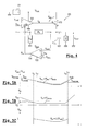
- Figure 1 shows a classic linear regulator 10 whose output delivers a regulated voltage Vout at a load Z.
- the load Z represents for example various radio circuits present in a mobile phone.
- Regulator 10 is powered electrically by a voltage Vbat delivered by a battery 1 and includes a differential amplifier 2 whose output drives the gate G of a transistor PMOS type regulation 3.
- Transistor 3 is typically a low resistance transistor series to the on state (drain-source resistance RdsON) and receives on its source S the voltage Vbat. Its drain D, connected to the output of regulator 10, is connected to the anode of a filtering and stabilizing capacitor Cst voltage Vout, arranged in parallel with the load Z.
- Amplifier 2 receives on its negative input a reference voltage Vref and on its positive input a feedback voltage Vfb (feedback). Voltage Vfb is a fraction of the voltage Vout brought back on the input of amplifier 2 via a divider bridge comprising two resistors R1, R2.
- FIG. 2 represents an embodiment classic amplifier 2.
- This includes a differential stage represented in the form of a block 5, receiving as input the voltages Vref and Vfb and polarized by a current generator 6.
- the output of the floor differential 5 drives the gate of a transistor 7 of the type NMOS connected between the amplifier output node 2 and the mass.
- Transistor 7 is polarized on its drain D by a current generator 8.
- the output node of the amplifier is connected to the supply voltage Vbat by a gate resistance Rg, which determines the amplifier gain and the maximum current it can output. So depending on the signal value delivered by the differential stage 5, the transistor 7 draws amplifier output to ground or the resistance Rg pulls the output upwards, i.e. the voltage Vbat.
- the control amplifier In an application such as food mobile phone, it is important that the control amplifier has a consumption as low as possible in order to preserve battery life.
- the resistance of grid Rg is chosen to be of high value, for example 100K ⁇ , to limit the current flowing in the stage Release.
- the currents delivered by the generators 6, 8 are adequately calibrated.
- the choice of resistance Rg and bias currents is the result of a compromise between the need to effectively pilot the transistor 3, which generally has a capacitance high grid parasite, and looking for a low consumption.
- this consumption typically of the order from 50 to 200 microamps, which is in itself acceptable when the battery is fully charged and the regulator operates in a steady state
- the present invention is is based on the premise that this consumption must by against being considered too high when the voltage of Vbat battery becomes weak and below the value nominal Voutnom of the output voltage. Such a fall of the voltage Vbat below the nominal voltage Voutnom can be temporary and due to a strong current consumption, or be due to the fact that the battery is discharged.
- the amplifier unnecessarily consumes current when the regulator operates in follower mode, since the regulating transistor is continuously in the on state and that a voltage regulation of Vout exit is no longer possible.
- the idea of present invention is to rock the amplifier regulation in a low standby mode consumption while maintaining in the state passing the regulating transistor.
- the present invention provides a voltage regulator comprising a transistor Regulation MOS and an amplifier whose output controls the gate of the regulation transistor as a function the difference between a reference voltage and a voltage feedback, the regulator comprising means to toggle the amplifier in a mode of ensures low current consumption when the deviation between supply voltage and output voltage of the regulator is less than a first threshold, while now on the gate of the regulating transistor a electrical potential to maintain the regulation transistor in the on state.
- the regulator includes a comparator arranged to compare the voltage supply and the regulator output voltage, and provide a standby signal to the amplifier when the difference between the supply voltage and the regulator output voltage is less than first threshold.
- the comparator has a switching hysteresis and cancels the amplifier standby signal when the difference between the supply voltage and the regulator output is above a second threshold greater than the first threshold.
- the amplifier includes a resistor connecting the output of the amplifier at the supply voltage, a switch is arranged in series with the resistor, the switch in series with the resistor is open when the amplifier is put on standby and closed in the opposite case.
- the amplifier includes current sources toggling in low mode current when the amplifier is put on standby.
- the amplifier includes a switch controlled by an activation signal standby to connect the gate of the transistor regulation at an electrical potential making the transistor on when the amplifier is turned on standby.
- the amplifier includes a stage of polarization of the grid of the regulating transistor, arranged to apply to the gate of the regulation transistor, when the amplifier is put on standby, a voltage which is determined so that the gate-source voltage of the regulating transistor be close to the voltage of threshold of the regulation transistor.
- the power supply amplifier power is removed in mode standby by a switch.
- the present invention also relates to a mobile phone including battery and circuits radio powered by a regulator according to the invention.
- the present invention also provides a method for managing the energy available in a battery feeding a load via a regulator voltage, the regulator comprising a MOS transistor regulation and an amplifier whose output controls the gate of the regulation transistor as a function of the difference between a reference voltage and a feedback voltage, process comprising a step consisting of monitor the difference between the supply voltage and the regulator output voltage, and a step consisting to switch the amplifier to a standby mode at low current consumption when the gap between the supply voltage and the output voltage of the regulator is less than a first threshold, while now the gate of the regulating transistor at a potential to maintain the transistor regulation in the on state.
- the consumption of the amplifier can be reduced in standby mode by disconnecting the output node of the supply voltage amplifier, reducing the current delivered by current sources internal to the amplifier, or removing the application of the supply voltage.
- FIG. 4 represents a regulator 20 according to the invention, supplied here by a voltage Vbat supplied by a battery 21.
- the regulator 20 includes as that of FIG. 1 a differential amplifier 22 whose output controls the gate of a transistor PMOS type regulation 23.
- the drain D of transistor 23 is connected to the output of regulator 20 and is connected to a stabilization capacity Cst in parallel with a load Z, these various elements being arranged as described in the preamble.
- the output voltage Vout is brought back to the positive input of amplifier 2 by via a divider bridge comprising two resistors R1, R2.
- the resistance R1 can be zero in the case of a direct feedback of the voltage of output Vout on the input of amplifier 22, the resistance R2 in this case being mathematically infinite.
- the reference voltage Vref applied to the input negative of amplifier 2 is for example a voltage so-called band-gap with good stability in temperature function, generated by means of diodes PN junction and current mirrors.
- the voltage Vref is thus independent of the voltage Vbat, on the condition to be less than the lowest voltage value Vbat.
- Amplifier 2 maintains the feedback voltage Vfb equal to the reference voltage Vref and the nominal output voltage Voutnom is equal to [(R1 + R2) Vref / R2].
- the amplifier 22 has a "normal" operating mode and a “standby” mode and switches from one to the other according to the value of a signal Vlc applied to an LCIN input provided for this purpose.
- Setting standby amplifier 22 consists, according to the invention, in placing the amplifier in a state of low power consumption while now the gate voltage Vg at a potential maintaining the regulation transistor 23 in the passing state.
- Various examples of realization of the amplifier 22 will be described later. We will consider by convention, in what follows, that the amplifier switches to standby mode when the signal Vlc goes to 1.
- the signal Vlc is delivered by a comparator 24 receiving on its positive input the output voltage Vout and on its negative input the supply voltage Vbat, the comparator 24 being supplied by the voltage Vbat.
- Comparator 24 is a threshold comparator Vd1 and here sets its output to 1 (signal Vlc) when the voltage differential Vd seen on its inputs, equal to the difference between the voltage Vbat and the voltage Vout, becomes below the threshold Vd1.
- comparator 24 has also, preferably, a switching hysteresis and resets its output to 0 when the differential voltage Vd goes up and becomes higher than a higher threshold Vd2 to Vd1.
- the thresholds Vd1, Vd2 are for example equal to 100 mV and 120mV, respectively.
- amplifier 22 switches to standby mode while holding the regulating transistor 23 in the on state, when the regulator 20 operates in follower mode due to voltage drop Vbat power supply below the nominal value Voutnom of the output voltage.
- FIGs 5A, 5B, 5C illustrate the operation of regulator 20 in follower mode and represent the voltages Vbat and Vout respectively, the voltage differential Vd and the signal Vlc.
- a decrease in the voltage Vbat from of its nominal value Vbatnom has no consequence on the regulated voltage Vout, which remains equal to Voutnom, as long as the voltage Vbat remains greater than Voutnom.
- the differential voltage Vd decreases in proportion to the voltage Vbat until an instant t2 where the voltage Vbat becomes substantially equal to Voutnom and causes the voltage Vout in its fall, the regulator then being unbalanced and operating in follower mode.
- the differential voltage Vd reaches a minimum value Vdmin which corresponds to the fall of voltage across the regulation transistor 23.
- This voltage drop Vdmin is in principle very small, by example 50 mV, because the regulating transistor of a LDO type regulator usually has a VdsON drain-source resistance in the very on state low. From time t2, the voltage Vout begins to decrease and follows the voltage Vbat, at the offset near the voltage Vdmin.
- the transition to follower mode is detected by comparator 24 at a time t1 preceding t2 but very close to t2, when the voltage differential Vd reaches the threshold Vd1 mentioned more high, chosen very close to the minimum Vdmin. So at at time t1, the signal Vlc goes to 1 (fig. 5C) and amplifier 2 is put on standby.
- the logical "1" of signal Vlc here is the voltage Vbat, which supplies the comparator 24.
- the voltage Vbat then goes back up to its nominal value, for example after recharging the battery 21 or regenerating natural of it when the current consumed decreases.
- the voltage Vbat exceeds the Voutnom value.
- the voltage differential Vd exceeds the threshold Vd2 and the amplifier 22 switches to its normal operating mode, the voltage Vout returning to its nominal value Voutnom.
- the amplifier 22a illustrated in FIG. 6 is of a structure similar to that of amplifier 2.
- the differential stage 5 polarized by the current generator 6, the output of which controls the NMOS transistor 7 polarized on its drain by the current generator 8, as well as the resistance Rg connecting the output node of amplifier 22a to the Vbat voltage.
- a switch 25, here a PMOS transistor is arranged in series with the resistance Rg.
- the transistor 25 receives on its gate the signal Vlc and is thus permanently in the on state when the regulator is operating in steady state, the signal Vlc being at 0 as indicated above.
- the amplifier 22b shown in FIG. 7 is almost identical to amplifier 22a.
- current generators 6, 8 have been replaced by current generators 6 ', 8' which are controlled by the signal Vlc and which deliver different currents according to the value of the signal Vlc.
- the respective currents I1 ', I2' delivered when the signal Vlc is at 1 are for example equal to half of the currents I1, I2 delivered when the signal Vlc is at 0.
- the currents I1 ', I2' are by example of 10 microamps and the currents I1, I2 of 20 microamps.
- the amplifier 22c of FIG. 8 is produced at starting from the amplifier 2 of FIG. 2, which we have not changed in its internal structure.
- the Vbat voltage is applied to the power input of amplifier 2 via a transistor PMOS 26 controlled by the Vlc signal.
- a transistor NMOS 27 driven by the Vlc signal is added between the amplifier 2 output and ground. So when signal Vlc is at 0 (balanced regulator), the transistor 26 is on and transistor 27 is blocked. Amplifier 2 works as if these two elements did not exist. When the signal Vlc is at 1 (regulator in follower mode), transistor 26 is blocked and transistor 27 is on. Amplifier 2 does not no longer receives the supply voltage Vbat and is completely off.
- the transistor 27 draws the amplifier output at 0 (voltage Vg) to maintain the regulating transistor 23 in the on state.
- This embodiment 22c therefore differs from the preceding 22a, 22b by the fact that in standby mode the voltage of gate Vg is not grounded by the transistor NMOS 2 of the output stage of amplifier 2, which is out of service, but by the additional transistor 27 meant for that purpose.
- the amplifier 22d represented in FIG. 9 comprises also amplifier 2 and transistor 26 ensuring switching off amplifier 2 when the signal Vlc is at 1.
- the pull-down transistor 27 (pull down) at the output of amplifier 22c is replaced by a 30 more advanced bias stage which maintains the output of amplifier 2 at a voltage Vg greater than ground when it is off.
- This voltage Vg is chosen so that the voltage source gate Vgs of the regulation transistor 23 or maintained in the vicinity of the threshold voltage Vtp of the transistor 23.
- the polarization step 30 comprises for example a first PMOS transistor 31 receiving the voltage Vbat on its source, connected by its drain to the source of a second PMOS transistor 32 whose drain is connected to the amplifier output node 22d.
- Transistors 31, 32 are arranged in diodes, each having its grid connected to its drain.
- the bias stage 30 includes a resistor 33 of high value in series with an NMOS transistor 34 driven by the Vlc signal.
- the signal Vlc is at 0 and the transistor 34 is also blocked.
- Amplifier 2 operates as if bias stage 30 did not exist not.
- the voltage Vg tends to 0
- signal Vlc goes to 1 and amplifier 2 is turned off.
- the two diode transistors 31, 32 become passers-by and each impose a voltage Vtp at their terminals, so the gate voltage Vg is in this case equal to [Vbat - (2Vtp)].
- the voltage Vgs of regulation transistor 23 is thus equal to 2Vtp in absolute value and is close to Vtp (at the value Vtp close, of the order of 0.7 V). Other methods are good heard possible to maintain the voltage Vg still closer to the threshold voltage Vtp.
- the advantage of this embodiment is that it does not fully discharge the stray capacitance of grid Cg of the regulation transistor 23, shown in lines dotted, which is usually of high value (100-200 picofarads) with a low regulation transistor resistance RdsON series. Indeed, when the voltage Vg is brought to ground, the Cg capacity is fully discharged during standby mode. If the voltage Vbat goes up suddenly, a delay in closing the transistor 23 (transistor blocking) occurs during return to regulated mode due to the charging time of the capacity Cg. Such a delay in closing reveals an overvoltage at the regulator output, because the voltage Vout continues to follow Vbat voltage beyond its nominal value Voutnom. Maintaining the voltage Vg no zero during standby mode, the grid capacity Cg does not not fully discharging and switching the mode Standby in regulated mode is done quickly, with a clear attenuation of the overvoltage phenomenon.
- each of the amplifiers 22a to 22d can be provided, to make other variants of production.
- the bias stage 30 of the 22d amplifier can be incorporated in the amplifiers 22a, 22b. It is also within reach of those skilled in the art of applying the principles and solutions exposed above to amplifier structures known other than that of amplifier 2 chosen here for example.
- the examples which have just been described relate to a regulator having a PMOS type regulation transistor, it enters as part of this application and it is at the scope of the skilled person to transpose the teaching of the present invention to regulators having a NMOS type regulation transistor.
Landscapes
- Engineering & Computer Science (AREA)
- Physics & Mathematics (AREA)
- Electromagnetism (AREA)
- General Physics & Mathematics (AREA)
- Radar, Positioning & Navigation (AREA)
- Automation & Control Theory (AREA)
- Continuous-Control Power Sources That Use Transistors (AREA)
Abstract
Description
- la figure 1 précédemment décrite est le schéma électrique d'un régulateur de tension classique,
- la figure 2 précédemment décrite est le schéma électrique d'un amplificateur présent dans le régulateur de la figure 1,
- les figures 3A à 3C représentent des signaux électriques et illustrent le fonctionnement du régulateur de tension lorsque la tension d'alimentation chute en dessous de la valeur nominale de la tension de sortie,
- la figure 4 est le schéma électrique d'un régulateur de tension selon l'invention,
- les figures 5A à 5C représentent des signaux électriques et illustrent le fonctionnement du régulateur selon l'invention en mode suiveur, et
- les figures 6 à 9 sont des schémas électriques de quatre variantes de réalisation d'un amplificateur selon l'invention présent dans le régulateur de la figure 4.
Claims (15)
- Régulateur de tension (20) comprenant un transistor MOS de régulation (23) et un amplificateur (22, 22a-22d) dont la sortie pilote la grille du transistor de régulation en fonction de l'écart entre une tension de référence (Vref) et une tension de contre-réaction (Vfb), caractérisé en ce qu'il comprend des moyens (6', 7', 24, 25, 27, 27, 30) pour faire basculer l'amplificateur dans un mode de veille à faible consommation de courant lorsque l'écart (Vd) entre la tension d'alimentation (Vbat) et la tension de sortie (Vout) du régulateur est inférieur à un premier seuil (Vd1), tout en maintenant sur la grille du transistor de régulation (23) un potentiel électrique permettant de maintenir le transistor de régulation dans l'état passant.
- Régulateur selon la revendication 1, comprenant un comparateur (24) agencé pour comparer la tension d'alimentation (Vbat) et la tension de sortie (Vout) du régulateur, et délivrer à l'amplificateur (22) un signal de mise en veille (Vlc=1) lorsque l'écart (Vd) entre la tension d'alimentation et la tension de sortie du régulateur est inférieur au premier seuil (Vd1).
- Régulateur selon la revendication 2, caractérisé en ce que le comparateur (24) présente une hystérésis de commutation et annule le signal de mise en veille de l'amplificateur (Vlc=0) lorsque l'écart (Vd) entre la tension d'alimentation et la tension de sortie du régulateur est supérieur à un second seuil (Vd2) supérieur au premier seuil (Vd1).
- Régulateur selon l'une des revendications 1 à 3, dans lequel l'amplificateur (22a, 22b) comprend une résistance (Rg) reliant la sortie de l'amplificateur à la tension d'alimentation (Vbat), caractérisé en ce qu'un interrupteur (25) est agencé en série avec la résistance (Rg) et en ce que ledit interrupteur agencé en série avec la résistance est ouvert lorsque l'amplificateur est mis en veille et fermé dans le cas contraire.
- Régulateur selon l'une des revendications 1 à 4, dans lequel l'amplificateur (22b) comprend des sources de courant (6', 8') basculant en mode faible courant lorsque l'amplificateur est mis en veille.
- Régulateur selon l'une des revendications 1 à 5, dans lequel l'amplificateur comprend un interrupteur (27) piloté par un signal de mise en veille (Vlc) pour connecter la grille du transistor de régulation (23) à un potentiel électrique rendant le transistor passant lorsque l'amplificateur est mis en veille.
- Régulateur selon l'une des revendications 1 à 6, dans lequel l'amplificateur (22d) comprend un étage (30) de polarisation de la grille du transistor de régulation (23), agencé pour appliquer sur la grille du transistor de régulation, lorsque l'amplificateur est mis en veille, une tension (Vg) qui est déterminée de manière que la tension grille-source (Vgs) du transistor de régulation soit proche de la tension de seuil (Vtp) du transistor de régulation.
- Régulateur selon l'une des revendications 6 et 7, dans lequel l'alimentation électrique de l'amplificateur (22c, 22d) est supprimée en mode veille par un interrupteur (26).
- Téléphone mobile comprenant une batterie et des circuits radio alimentés par l'intermédiaire d'un régulateur (20) selon l'une des revendications 1 à 8.
- Procédé de gestion de l'énergie disponible dans une batterie (21) alimentant une charge (Z) par l'intermédiaire d'un régulateur de tension (20), le régulateur comprenant un transistor MOS de régulation (23) et un amplificateur (22) dont la sortie pilote la grille du transistor de régulation en fonction de l'écart entre une tension de référence (Vref) et une tension de contre-réaction (Vfb), procédé caractérisé en ce qu'il comprend une étape consistant à surveiller l'écart (Vd) entre la tension d'alimentation (Vbat) et la tension de sortie (Vout) du régulateur, et une étape consistant à faire basculer l'amplificateur (22) dans un mode veille à faible consommation de courant lorsque l'écart (Vd) entre la tension d'alimentation (Vbat) et la tension de sortie (Vout) du régulateur est inférieur à un premier seuil (Vd1), tout en maintenant la grille du transistor de régulation (23) à un potentiel permettant de maintenir le transistor de régulation dans l'état passant.
- Procédé selon la revendication 10, caractérisé en ce que l'on réactive l'amplificateur (20) lorsque l'écart (Vd) entre la tension d'alimentation et la tension de sortie du régulateur est supérieur à un second seuil (Vd2) supérieur au premier seuil (Vd1).
- Procédé selon l'une des revendications 10 et 11, dans lequel on réduit la consommation de l'amplificateur (22, 22a, 22b) en mode veille en déconnectant (25, Vlc=1) le noeud de sortie de l'amplificateur de la tension d'alimentation (Vbat).
- Procédé selon l'une des revendications 10 à 12, dans lequel on réduit la consommation de l'amplificateur (22, 22b) en mode veille en diminuant le courant délivré par des sources de courant (6', 8') internes à l'amplificateur.
- Procédé selon l'une des revendications 10 et 11, dans lequel on supprime l'application de la tension d'alimentation à l'amplificateur en mode veille.
- Procédé selon l'une des revendications 10 à 14, dans lequel on applique sur la grille du transistor de régulation (23), lorsque l'amplificateur est mis en veille, une tension (Vg) qui est déterminée de manière que la tension grille-source (Vgs) du transistor de régulation soit proche de la tension de seuil (Vtp) du transistor de régulation.
Applications Claiming Priority (2)
| Application Number | Priority Date | Filing Date | Title |
|---|---|---|---|
| FR0004675A FR2807846A1 (fr) | 2000-04-12 | 2000-04-12 | Regulateur de tension a faible consommation electrique |
| FR0004675 | 2000-04-12 |
Publications (2)
| Publication Number | Publication Date |
|---|---|
| EP1148404A1 true EP1148404A1 (fr) | 2001-10-24 |
| EP1148404B1 EP1148404B1 (fr) | 2005-11-02 |
Family
ID=8849155
Family Applications (1)
| Application Number | Title | Priority Date | Filing Date |
|---|---|---|---|
| EP01108243A Expired - Lifetime EP1148404B1 (fr) | 2000-04-12 | 2001-03-31 | Régulateur de tension à faible consommation électrique |
Country Status (4)
| Country | Link |
|---|---|
| US (1) | US6501253B2 (fr) |
| EP (1) | EP1148404B1 (fr) |
| DE (1) | DE60114500D1 (fr) |
| FR (1) | FR2807846A1 (fr) |
Families Citing this family (31)
| Publication number | Priority date | Publication date | Assignee | Title |
|---|---|---|---|---|
| FR2830091B1 (fr) * | 2001-09-25 | 2004-09-10 | St Microelectronics Sa | Regulateur de tension incorporant une resistance de stabilisation et un circuit de limitation du courant de sortie |
| US6979984B2 (en) * | 2003-04-14 | 2005-12-27 | Semiconductor Components Industries, L.L.C. | Method of forming a low quiescent current voltage regulator and structure therefor |
| US7085943B2 (en) * | 2003-09-26 | 2006-08-01 | Freescale Semiconductor, Inc. | Method and circuitry for controlling supply voltage in a data processing system |
| US7446514B1 (en) | 2004-10-22 | 2008-11-04 | Marvell International Ltd. | Linear regulator for use with electronic circuits |
| JP4651428B2 (ja) * | 2005-03-28 | 2011-03-16 | ローム株式会社 | スイッチングレギュレータ及びこれを備えた電子機器 |
| US7450354B2 (en) * | 2005-09-08 | 2008-11-11 | Aimtron Technology Corp. | Linear voltage regulator with improved responses to source transients |
| US8049551B2 (en) * | 2008-06-17 | 2011-11-01 | Monolithic Power Systems, Inc. | Charge pump for switched capacitor circuits with slew-rate control of in-rush current |
| JP5489502B2 (ja) * | 2009-03-19 | 2014-05-14 | キヤノン株式会社 | 電源装置 |
| US9134741B2 (en) * | 2009-06-13 | 2015-09-15 | Triune Ip, Llc | Dynamic biasing for regulator circuits |
| JP5501696B2 (ja) * | 2009-08-19 | 2014-05-28 | オリンパス株式会社 | 実装装置および実装方法 |
| US8022770B1 (en) * | 2010-05-27 | 2011-09-20 | Skyworks Solutions, Inc. | System and method for preventing power amplifier supply voltage saturation |
| US8384465B2 (en) | 2010-06-15 | 2013-02-26 | Aeroflex Colorado Springs Inc. | Amplitude-stabilized even order pre-distortion circuit |
| US20110309808A1 (en) | 2010-06-16 | 2011-12-22 | Aeroflex Colorado Springs Inc. | Bias-starving circuit with precision monitoring loop for voltage regulators with enhanced stability |
| TWI420275B (zh) * | 2010-07-13 | 2013-12-21 | Sitronix Technology Corp | Switching capacitor voltage regulator |
| US20120194150A1 (en) * | 2011-02-01 | 2012-08-02 | Samsung Electro-Mechanics Company | Systems and methods for low-battery operation control in portable communication devices |
| CN102298408A (zh) * | 2011-04-22 | 2011-12-28 | 上海宏力半导体制造有限公司 | 稳压电路 |
| TWM422090U (en) * | 2011-08-29 | 2012-02-01 | Richtek Technology Corp | Linear regulator and control circuit thereof |
| CN102545855B (zh) * | 2012-01-17 | 2017-04-05 | 南京航空航天大学 | 基于闭环控制的功率开关管驱动方法及系统 |
| JP2013186721A (ja) * | 2012-03-08 | 2013-09-19 | Toyota Motor Corp | 電源回路とそれを用いた電子制御装置 |
| FR2988869A1 (fr) * | 2012-04-03 | 2013-10-04 | St Microelectronics Rousset | Regulateur a faible chute de tension a etage de sortie ameliore |
| JP6008678B2 (ja) * | 2012-09-28 | 2016-10-19 | エスアイアイ・セミコンダクタ株式会社 | ボルテージレギュレータ |
| US9201436B2 (en) * | 2013-07-22 | 2015-12-01 | Entropic Communications, Llc | Adaptive LDO regulator system and method |
| EP2846213B1 (fr) * | 2013-09-05 | 2023-05-03 | Renesas Design Germany GmbH | Procédé et appareil permettant de limiter le courant d'appel pour le démarrage d'un régulateur à faible chute de tension |
| US9177617B2 (en) * | 2013-10-08 | 2015-11-03 | Cypress Semiconductor Corporation | Methods circuits apparatuses and systems for providing current to a non-volatile memory array and non-volatile memory devices produced accordingly |
| EP3051378B1 (fr) * | 2015-01-28 | 2021-05-12 | ams AG | Circuit régulateur à faible chute de tension et procédé pour commander une tension d'un tel circuit |
| CN105549673B (zh) * | 2015-12-25 | 2017-01-25 | 上海华虹宏力半导体制造有限公司 | 双模切换式ldo电路 |
| US10761549B2 (en) * | 2017-01-12 | 2020-09-01 | Microsemi Corporation | Voltage sensing mechanism to minimize short-to-ground current for low drop-out and bypass mode regulators |
| DE102017201705B4 (de) * | 2017-02-02 | 2019-03-14 | Dialog Semiconductor (Uk) Limited | Spannungsregler mit Ausgangskondensatormessung |
| CN109871059B (zh) * | 2019-02-25 | 2020-07-14 | 华中科技大学 | 一种超低电压ldo电路 |
| CN110011536A (zh) * | 2019-05-06 | 2019-07-12 | 核芯互联(北京)科技有限公司 | 一种新型电源电路 |
| US11625056B2 (en) * | 2021-03-12 | 2023-04-11 | Steradian Semiconductors Private Limited | Low noise voltage regulator |
Citations (5)
| Publication number | Priority date | Publication date | Assignee | Title |
|---|---|---|---|---|
| US4319179A (en) * | 1980-08-25 | 1982-03-09 | Motorola, Inc. | Voltage regulator circuitry having low quiescent current drain and high line voltage withstanding capability |
| EP0501418A2 (fr) * | 1991-02-27 | 1992-09-02 | STMicroelectronics S.r.l. | Régulateur de tension a faible chute de tension. |
| US5355077A (en) * | 1992-04-27 | 1994-10-11 | Dell U.S.A., L.P. | High efficiency regulator with shoot-through current limiting |
| EP0678963A2 (fr) * | 1994-04-18 | 1995-10-25 | Nokia Mobile Phones Ltd. | Procédé et dispositif de commande de la consommation de puissance d'un appareil électronique |
| US6046577A (en) * | 1997-01-02 | 2000-04-04 | Texas Instruments Incorporated | Low-dropout voltage regulator incorporating a current efficient transient response boost circuit |
Family Cites Families (2)
| Publication number | Priority date | Publication date | Assignee | Title |
|---|---|---|---|---|
| FR2807847B1 (fr) * | 2000-04-12 | 2002-11-22 | St Microelectronics Sa | Regulateur lineaire a faible surtension en regime transitoire |
| US6246221B1 (en) * | 2000-09-20 | 2001-06-12 | Texas Instruments Incorporated | PMOS low drop-out voltage regulator using non-inverting variable gain stage |
-
2000
- 2000-04-12 FR FR0004675A patent/FR2807846A1/fr active Pending
-
2001
- 2001-03-31 DE DE60114500T patent/DE60114500D1/de not_active Expired - Lifetime
- 2001-03-31 EP EP01108243A patent/EP1148404B1/fr not_active Expired - Lifetime
- 2001-04-04 US US09/826,299 patent/US6501253B2/en not_active Expired - Lifetime
Patent Citations (5)
| Publication number | Priority date | Publication date | Assignee | Title |
|---|---|---|---|---|
| US4319179A (en) * | 1980-08-25 | 1982-03-09 | Motorola, Inc. | Voltage regulator circuitry having low quiescent current drain and high line voltage withstanding capability |
| EP0501418A2 (fr) * | 1991-02-27 | 1992-09-02 | STMicroelectronics S.r.l. | Régulateur de tension a faible chute de tension. |
| US5355077A (en) * | 1992-04-27 | 1994-10-11 | Dell U.S.A., L.P. | High efficiency regulator with shoot-through current limiting |
| EP0678963A2 (fr) * | 1994-04-18 | 1995-10-25 | Nokia Mobile Phones Ltd. | Procédé et dispositif de commande de la consommation de puissance d'un appareil électronique |
| US6046577A (en) * | 1997-01-02 | 2000-04-04 | Texas Instruments Incorporated | Low-dropout voltage regulator incorporating a current efficient transient response boost circuit |
Also Published As
| Publication number | Publication date |
|---|---|
| FR2807846A1 (fr) | 2001-10-19 |
| DE60114500D1 (de) | 2005-12-08 |
| US6501253B2 (en) | 2002-12-31 |
| US20010030530A1 (en) | 2001-10-18 |
| EP1148404B1 (fr) | 2005-11-02 |
Similar Documents
| Publication | Publication Date | Title |
|---|---|---|
| EP1148404B1 (fr) | Régulateur de tension à faible consommation électrique | |
| EP1148405B1 (fr) | Régulateur linéaire à faible surtension en régime transitoire | |
| FR3051570B1 (fr) | Dispositif de regulation a faible chute de tension, en particulier capable de supporter des tensions d'alimentation compatibles avec la norme usb type c | |
| EP0847124B1 (fr) | Alimentation de secours destinée à suppléer provisoirement à une carence d'une source d'alimentation principale | |
| EP2256578A1 (fr) | Régulateur de tension à faible tension de dechet et faible courant de repos | |
| FR2819064A1 (fr) | Regulateur de tension a stabilite amelioree | |
| JPH0644774A (ja) | 改良式チップ・オン電源制御装置を有する集積回路 | |
| EP1326154B1 (fr) | Pompe à charge à très large plage de tension de sortie | |
| FR3032309A1 (fr) | Circuit de regulation de tension adapte aux fortes et faibles puissances | |
| US20060176025A1 (en) | Charging control circuit and charging device | |
| FR3099321A1 (fr) | Alimentation à découpage | |
| FR3102580A1 (fr) | Régulateur de tension | |
| EP3576268B1 (fr) | Circuit électronique d'alimentation | |
| EP2932588B1 (fr) | Circuit de comparaison d'une tension a un seuil et conversion d'energie electrique | |
| EP3696645B1 (fr) | Dispositif de fourniture d'une puissance d'alimentation | |
| EP2722727B1 (fr) | Alimentation d'une charge à potentiel flottant | |
| US7312450B2 (en) | Infrared detecting device | |
| FR3119469A1 (fr) | Interface USB PD | |
| EP3771080A1 (fr) | Démarrage d'une alimentation à découpage | |
| EP0538121B1 (fr) | Dispositif pour générer une tension de programmation d'une mémoire permanente programmable, notamment de type EPROM, procédé et mémoire s'y rapportant | |
| WO2021250254A1 (fr) | Convertisseur de tension dc/dc avec dispositif de precharge | |
| FR3147392A1 (fr) | Régulateur à pompe de charge | |
| EP4517473B1 (fr) | Régulateur de tension | |
| FR3091057A1 (fr) | Dispositif de pré-charge et convertisseur de tension comportant un tel dispositif. | |
| FR3131805A1 (fr) | Capteur de lumière |
Legal Events
| Date | Code | Title | Description |
|---|---|---|---|
| PUAI | Public reference made under article 153(3) epc to a published international application that has entered the european phase |
Free format text: ORIGINAL CODE: 0009012 |
|
| AK | Designated contracting states |
Kind code of ref document: A1 Designated state(s): AT BE CH CY DE DK ES FI FR GB GR IE IT LI LU MC NL PT SE TR Kind code of ref document: A1 Designated state(s): DE FR GB IT |
|
| AX | Request for extension of the european patent |
Free format text: AL;LT;LV;MK;RO;SI |
|
| RAP1 | Party data changed (applicant data changed or rights of an application transferred) |
Owner name: STMICROELECTRONICS S.A. |
|
| 17P | Request for examination filed |
Effective date: 20020306 |
|
| AKX | Designation fees paid |
Free format text: DE FR GB IT |
|
| RAP1 | Party data changed (applicant data changed or rights of an application transferred) |
Owner name: STMICROELECTRONICS SA |
|
| GRAP | Despatch of communication of intention to grant a patent |
Free format text: ORIGINAL CODE: EPIDOSNIGR1 |
|
| GRAS | Grant fee paid |
Free format text: ORIGINAL CODE: EPIDOSNIGR3 |
|
| GRAA | (expected) grant |
Free format text: ORIGINAL CODE: 0009210 |
|
| AK | Designated contracting states |
Kind code of ref document: B1 Designated state(s): DE FR GB IT |
|
| PG25 | Lapsed in a contracting state [announced via postgrant information from national office to epo] |
Ref country code: IT Free format text: LAPSE BECAUSE OF FAILURE TO SUBMIT A TRANSLATION OF THE DESCRIPTION OR TO PAY THE FEE WITHIN THE PRESCRIBED TIME-LIMIT;WARNING: LAPSES OF ITALIAN PATENTS WITH EFFECTIVE DATE BEFORE 2007 MAY HAVE OCCURRED AT ANY TIME BEFORE 2007. THE CORRECT EFFECTIVE DATE MAY BE DIFFERENT FROM THE ONE RECORDED. Effective date: 20051102 |
|
| REG | Reference to a national code |
Ref country code: GB Ref legal event code: FG4D Free format text: NOT ENGLISH |
|
| REF | Corresponds to: |
Ref document number: 60114500 Country of ref document: DE Date of ref document: 20051208 Kind code of ref document: P |
|
| PG25 | Lapsed in a contracting state [announced via postgrant information from national office to epo] |
Ref country code: DE Free format text: LAPSE BECAUSE OF FAILURE TO SUBMIT A TRANSLATION OF THE DESCRIPTION OR TO PAY THE FEE WITHIN THE PRESCRIBED TIME-LIMIT Effective date: 20060203 |
|
| GBT | Gb: translation of ep patent filed (gb section 77(6)(a)/1977) |
Effective date: 20060206 |
|
| PLBE | No opposition filed within time limit |
Free format text: ORIGINAL CODE: 0009261 |
|
| STAA | Information on the status of an ep patent application or granted ep patent |
Free format text: STATUS: NO OPPOSITION FILED WITHIN TIME LIMIT |
|
| 26N | No opposition filed |
Effective date: 20060803 |
|
| GBPC | Gb: european patent ceased through non-payment of renewal fee |
Effective date: 20070331 |
|
| PG25 | Lapsed in a contracting state [announced via postgrant information from national office to epo] |
Ref country code: GB Free format text: LAPSE BECAUSE OF NON-PAYMENT OF DUE FEES Effective date: 20070331 |
|
| PGFP | Annual fee paid to national office [announced via postgrant information from national office to epo] |
Ref country code: FR Payment date: 20070730 Year of fee payment: 7 |
|
| PGFP | Annual fee paid to national office [announced via postgrant information from national office to epo] |
Ref country code: GB Payment date: 20060329 Year of fee payment: 6 |
|
| REG | Reference to a national code |
Ref country code: FR Ref legal event code: ST Effective date: 20081125 |
|
| PG25 | Lapsed in a contracting state [announced via postgrant information from national office to epo] |
Ref country code: FR Free format text: LAPSE BECAUSE OF NON-PAYMENT OF DUE FEES Effective date: 20080331 |