US7312450B2 - Infrared detecting device - Google Patents
Infrared detecting device Download PDFInfo
- Publication number
- US7312450B2 US7312450B2 US10/536,980 US53698005A US7312450B2 US 7312450 B2 US7312450 B2 US 7312450B2 US 53698005 A US53698005 A US 53698005A US 7312450 B2 US7312450 B2 US 7312450B2
- Authority
- US
- United States
- Prior art keywords
- circuit
- current
- signal
- switch
- voltage
- Prior art date
- Legal status (The legal status is an assumption and is not a legal conclusion. Google has not performed a legal analysis and makes no representation as to the accuracy of the status listed.)
- Expired - Fee Related, expires
Links
Images


Classifications
-
- G—PHYSICS
- G01—MEASURING; TESTING
- G01J—MEASUREMENT OF INTENSITY, VELOCITY, SPECTRAL CONTENT, POLARISATION, PHASE OR PULSE CHARACTERISTICS OF INFRARED, VISIBLE OR ULTRAVIOLET LIGHT; COLORIMETRY; RADIATION PYROMETRY
- G01J5/00—Radiation pyrometry, e.g. infrared or optical thermometry
- G01J5/10—Radiation pyrometry, e.g. infrared or optical thermometry using electric radiation detectors
- G01J5/34—Radiation pyrometry, e.g. infrared or optical thermometry using electric radiation detectors using capacitors, e.g. pyroelectric capacitors
- G01J5/35—Electrical features thereof
-
- G—PHYSICS
- G01—MEASURING; TESTING
- G01V—GEOPHYSICS; GRAVITATIONAL MEASUREMENTS; DETECTING MASSES OR OBJECTS; TAGS
- G01V8/00—Prospecting or detecting by optical means
- G01V8/10—Detecting, e.g. by using light barriers
Definitions
- the invention relates to an infrared detecting device.
- Infrared detecting devices are specially used in different electrical products which efficiently save energy while detecting a human body.
- a prior art device described Japanese Patent Publication No. 11-83624 is comprised of a pyroelectric element, an I/V conversion circuit, a voltage amplification circuit, a detection circuit and an output circuit.
- the pyroelectric element is operable to generate a micro current signal in response to variation of incoming infrared radiation from detection area through condenser lens or the like.
- the I/V conversion circuit converts the current signal from the pyroelectric element into a voltage signal.
- the voltage amplification circuit selectively amplifies components with prescribed frequencies of the voltage signal to issue a components-amplified voltage.
- the detection circuit is comprised of, for example, a window comparator and provides a comparison between the components-amplified voltage and a prescribed detection threshold voltage to issue a detection signal of the infrared radiation.
- the detection threshold voltage is a window threshold with a higher threshold voltage and a lower threshold voltage.
- the output circuit is comprised of, for example, level shift circuit or the like and issues an output signal in response to the detection signal.
- This infrared detecting device issues the output signal for representing detection of the infrared radiation (e.g., human body) when the components-amplified voltage is less or more than the window threshold range.
- the device also issues the output signal for representing non-detection of the infrared radiation when the components-amplified voltage is converged within the window threshold range.
- a prior art device described Japanese Patent Publication No. 2002-156281 comprises a battery as a power source in addition to the pyroelectric element, the I/V conversion circuit, the voltage amplification circuit, the detection circuit and the output circuit.
- This infrared detecting device provides a rated current as a drive current to I/V conversion circuit, the voltage amplification circuit, the detection circuit and the output circuit when voltage of the I/V conversion circuit exceeds a prescribed voltage.
- the device When the voltage of the I/V conversion circuit is equal to or lower than the prescribed voltage, the device provides a smaller current than the rated current as the drive current to those circuits. In this case, current consumption (drive current) can be reduced.
- An object of the present invention is to reduce current consumption while keeping the performance or behavior of the circuits in stable state.
- An infrared detecting device of the present invention comprises a pyroelectric element, an I/V conversion circuit, a voltage amplification circuit, a detection circuit, an output circuit and a drive power supply circuit.
- the pyroelectric element generates a current signal based on incoming infrared radiation.
- the I/V conversion circuit converts the current signal into a voltage signal.
- the voltage amplification circuit selectively amplifies components with prescribed frequencies (prescribed frequencies components) of the voltage signal to issue a components-amplified voltage.
- the detection circuit provides a comparison between the components-amplified voltage and a prescribed detection threshold voltage to issue a detection signal of the infrared radiation.
- the output circuit issues an output signal based on the detection signal.
- the drive power supply circuit supplies a drive current to each of signal circuits comprised of the I/V conversion circuit, the voltage amplification circuit, the detection circuit and the output circuit.
- the drive power supply circuit is comprised of a current generating circuit and a distribution circuit.
- the current generating circuit includes a reference current source, a fixed current source and a variable current source.
- the reference current source generates a reference current.
- the fixed current source provides a fixed current based on the reference current.
- the variable current source provides a variable current varying with the reference current.
- the distribution circuit distributes the drive current to a part of the signal circuits based on the current from the fixed current source.
- the distribution circuit also distributes the drive current to the remaining part of the signal circuits based on the current from the variable current source.
- the drive power supply circuit may comprise a plural of the variable current source, each of which is individually connected to each circuit of the remaining part of the signal circuits. In this case, since the drive current to each of the remaining part can be individually changed, the drive current can be preferably reduced to low level.
- the drive power supply circuit may comprise a terminal for receiving a changeover signal.
- the variable current source may step the variable current up or down to any of prescribed different currents in accordance with the changeover signal received at the terminal. Since drive current can be changed over in accordance with the changeover signal, current consumption can be adaptively reduced.
- the variable current source may step the variable current up or down to any of prescribed different currents based on variation of power voltage.
- the drive current can be preferably reduced based on the variation of the power voltage.
- variable current source may step the variable current up or down to any of prescribed different currents based on variation in ambient temperature.
- the drive current can be preferably reduced based on the variation in ambient temperature.
- the voltage amplification circuit may comprise a differential stage and an output stage.
- the distribution circuit may distribute the drive current to the differential stage or the output stage based on the current from said variable current source, or distribute same or different current as the drive current to the differential stage and the output stage based on the current from said variable current source.
- the infrared detecting device may further comprise a suppression circuit and the drive power supply circuit may comprise a current changeover circuit.
- This current changeover circuit provides a first changeover signal to the variable current source when the components-amplified voltage is closer to a reference level than a transition threshold voltage. This transition threshold voltage is set to be closer to the reference level than the detection threshold voltage.
- the current changeover circuit also provides a second changeover signal to the variable current source when the components-amplified voltage is further from the reference level than the transition threshold voltage.
- the variable current source steps the variable current down to a current smaller than a rated current of prescribed different currents based on the first changeover signal.
- the variable current source also steps the variable current up to the rated current based on the second changeover signal.
- the suppression circuit starts suppression of output of any circuit or circuits included in the signal circuits in order to suppress the output signal of the output circuit.
- the suppression is started from a start point in time on or before which the variable current source steps up or down the variable current.
- the suppression circuit also releases the suppression after a prescribed time period. In this case, it becomes possible to prevent false operation due to variation when the drive current is changed over.
- the suppression circuit may comprise a resistor, a constant voltage supply circuit, a switch and a switch controlling circuit.
- the resistor is connected in series between the voltage amplification circuit and the detection circuit.
- the constant voltage supply circuit supplies a constant voltage between the resistor and the detection circuit through the switch.
- the switch is connected between the constant voltage supply circuit and a pathway from the resistor to the detection circuit.
- the switch also opens or closes a pathway from the constant voltage supply circuit to the resistor and the detection circuit in response to OFF or ON signal from the switch controlling circuit respectively.
- the switch controlling circuit provides the ON signal to the switch from the start point.
- the switch controlling circuit also provides the OFF signal to the switch after the time period.
- the voltage amplification circuit may comprise an operational amplifier and a feedback resistor, and the suppression circuit may comprise a switch and a switch controlling circuit.
- the operational amplifier has a positive input terminal, a negative input terminal and an output terminal.
- the feedback resistor is connected between the output terminal and one of the input terminals.
- the switch is connected in parallel with the feedback resistor.
- the switch also opens or closes its parallel pathway in response to OFF or ON signal from the switch controlling circuit respectively.
- the switch controlling circuit provides the ON signal to the switch from the start point.
- the switch controlling circuit also provides the OFF signal to the switch after the time period. Since output of the voltage amplification circuit is suppressed at 1 ⁇ input voltage of the voltage amplification circuit during the time period, it becomes possible to prevent false operation due to variation when the drive current is changed over.
- the suppression circuit may comprise a resistor, a switch, a constant voltage supply circuit and a switch controlling circuit.
- the switch is connected between the voltage amplification circuit and the detection circuit.
- the switch also opens or closes a pathway from the voltage amplification circuit to the detection circuit in response to OFF or ON signal from the switch controlling circuit respectively.
- the constant voltage supply circuit supplies a constant voltage between the switch and the detection circuit through the resistor.
- the switch controlling circuit provides the OFF signal to the switch from the start point.
- the switch controlling circuit also provides the ON signal to the switch after the time period. Since the pathway is opened during the time period, it becomes possible to prevent false operation due to variation when the drive current is changed over.
- the suppression circuit may comprise a constant voltage supply circuit, a switch and a switch controlling circuit.
- the constant voltage supply circuit supplies a constant voltage to the detection circuit through the switch.
- the switch exists at a junction connecting the constant voltage supply circuit, the voltage amplification circuit, and the detection circuit.
- the switch also closes or opens a pathway (hereinafter referred to as a “first pathway”) between the constant voltage supply circuit and the detection circuit in response to suppression or unsuppression signal from the switch controlling circuit respectively.
- the switch also opens or closes a pathway (hereinafter referred to as a “second pathway”) between the voltage amplification circuit and the detection circuit in response to the suppression or the unsuppression signal respectively.
- the switch controlling circuit provides the suppression signal to the switch from the start point.
- the switch also provides the unsuppression signal to the switch after the time period. Since the first and the second pathways are closed and opened during the time period, it becomes possible to prevent false operation due to variation when the drive current is changed over.
- the suppression circuit may comprise a switch and a switch controlling circuit.
- the switch is connected between the detection circuit and the output circuit.
- the switch also opens or closes a pathway between the detection circuit and the output circuit in response to OFF or ON signal from the switch controlling circuit respectively.
- the switch controlling circuit provides the OFF signal to the switch from the start point.
- the switch controlling circuit also provides the ON signal to the switch after the time period. Since the pathway is opened during the time period, it becomes possible to prevent false operation due to variation when the drive current is changed over.
- the switch controlling circuit may issue the second changeover signal so that the variable current source increases the variable current to the biggest rated current while stepping up from smallest current of the different currents according to the second changeover signal.
- the switch controlling circuit may also issue the first changeover signal so that the variable current source decreases the variable current to the smallest current while stepping down from the rated current of the different currents according to the first changeover signal. Since the variable current is increased or decreased by sequential step up or down (i.e. discrete up or down) operation which can reduce variation it becomes possible to preferably prevent false operation due to variation when the drive current is changed over.
- FIG. 1 is an electrical diagram of an infrared detecting device of a first embodiment according to the present invention
- FIG. 2 is an electrical diagram of a voltage amplification circuit in the arrangement of FIG. 1 ;
- FIG. 3 is an electrical diagram of an operational amplifier in the arrangement of FIG. 2 ;
- FIG. 4 is a graph of reference current in the operational amplifier versus variation of power voltage
- FIG. 5 is an electrical diagram of an alternate embodiment
- FIG. 7 is an electrical diagram of a current changeover circuit, a current generating circuit and a distribution circuit in the arrangement of FIG. 6 ;
- FIG. 8 is an electrical diagram showing a part of an infrared detecting device of a third embodiment according to the present invention.
- FIG. 9 is a graph of current consumption versus variation of power voltage in the device of FIG. 8 ;
- FIG. 10 is a graph of current consumption of an alternate embodiment versus variation of power voltage
- FIG. 11 is an electrical diagram of an infrared detecting device of a fourth embodiment according to the present invention.
- FIG. 12 is a timing diagram showing operation of the device of FIG. 11 ;
- FIG. 13 is an electrical diagram 11 ; showing a part of an infrared detecting device of a fifth embodiment according to the present invention.
- FIG. 14 is an electrical diagram showing a part of an infrared detecting device of a sixth embodiment according to the present invention.
- FIG. 15 is a timing diagram showing operation of a suppression circuit of the device of FIG. 14 ;
- FIG. 16 is an electrical diagram showing a part of an infrared detecting device of a seventh embodiment according to the present invention.
- FIG. 17 is an electrical diagram showing a part of an infrared detecting device of a eighth embodiment according to the present invention.
- FIG. 18 is a timing diagram showing operation of an alternate embodiment
- FIG. 19 is an electrical diagram showing a part of an infrared detecting device of a ninth embodiment according to the present invention.
- FIG. 20 is a timing diagram showing operation of the device of FIG. 19 .
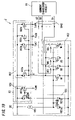
- FIG. 1 shows an infrared detecting device A of a first embodiment according to the present invention.
- the device A comprises a drive power supply circuit 10 as a characteristic of the embodiment in addition to comprising a pyroelectric element 15 , an I/V conversion circuit 16 , a voltage amplification circuit 17 , a detection circuit 18 and an output circuit 19 in the same way as the prior art devices.
- the above-mentioned prior art device has a limitation in reduction of current consumption of circuits 16 - 19 in order to secure a certain additional coverage for the ability of current supply. This point is explained in detail with reference to FIGS. 2 and 3 .
- the voltage amplification circuit 17 as shown in FIG. 2 comprises an operational amplifier 170 and resistors 171 and 172 .
- the amplifier 170 has a positive input terminal, a negative input terminal and an output terminal.
- a reference voltage Vref is applied to the positive input terminal.
- the resistor (feedback resistor) 171 is connected between the negative input terminal and the output terminal.
- the resistor 172 is connected between the I/V conversion circuit 16 and the negative input terminal of the amplifier 170 .
- the amplifier 170 as shown in FIG. 3 is constructed with a differential stage 170 a , an output stage 170 b and a constant current stage 170 c .
- This stage 170 c comprises transistors 170 d - 170 i which construct mirror circuits.
- the stage 170 c also provides power to the differential stage 170 a and output stage 170 b .
- the transistor 170 d is a PMOS depletion type of transistor.
- Each of the transistors 170 f , 170 h and 170 i is a PMOS enhancement type of transistor.
- Each of the transistors 170 e and 170 g is a NMOS enhancement type of transistor.
- the resistors 171 and 172 are set to 5 M Ohms and 200 K Ohms respectively, and thereby an voltage amplification rate of the amplifier 170 is set to 25 times (5 M Ohms/200 K Ohms).
- the ratio of current mirror of the stage 170 c is set in order that a reference current of 200 nA flows into the transistor 170 d while a drive current 200 nA and 400 nA flow into the stages 170 a and 170 b respectively, when power voltage is 3 V.
- the current into the transistor 170 d as shown in FIGS. 3 and 4 is reduced to approximately the half (from 200 nA to 100 nA).
- the output current ability of the amplifier 170 is also reduced to the half (from 400 nA to 200 nA). Therefore, when input signal of the amplifier 170 is greater than the upper end of the output current ability, the amplifier 170 cannot amplify the input signal in accordance with the voltage amplification rate. As a result, the secureness of the additional coverage and the reduction of the current consumption appear to be a contradictory problem.
- the circuit 10 as shown in FIG. 1 comprises a current changeover circuit 11 , a current generating circuit 12 and a distribution circuit 13 .
- the circuit 10 also supplies a drive current to each of signal circuits comprised of circuits 16 - 19 .
- This circuit 10 is characterized by independent current mirror circuits which are individually designed for the voltage amplification circuit 17 , the detection circuit 18 and the output circuit 19 . And these current mirror circuits change the dive current for each of the circuits 17 - 19 .
- the current changeover circuit 11 issues changeover signals for changeover of the dive current to the above-mentioned each circuit.
- the current generating circuit 12 is comprised of a reference current source 120 , a fixed current source 121 and variable current sources 122 - 124 .
- the circuit 12 generates a fixed current and variable currents.
- the reference current source 120 generates a reference current.
- the fixed current source 121 is comprised of a current mirror circuit with a terminal T 121 .
- the source 121 provides the distribution circuit 13 through the terminal T 121 with the fixed current based on the reference current from the reference current source 120 .
- the variable current sources 122 - 124 are comprised of current mirror circuits with terminals T 122 -T 124 respectively.
- Each variable current source provides the distribution circuit 13 through its terminal with the variable current stepped up or down to any of different currents based on the reference current. For example, the different currents are set to one, two, three times of the reference current.
- the fixed current source 121 is constructed with NMOS transistors 121 a and 121 b .
- the transistor 121 a is connected between the reference current source 120 and ground.
- the transistor 121 b is connected between the terminal T 121 and ground. Gates of these transistors 121 a and 121 b are also connected each other, while the gates are connected to a drain of the transistor 121 a .
- This source 121 provides to the distribution circuit 13 through the terminal T 121 with a current obtained by increasing or decreasing the reference current at a ratio of current mirror. This ratio of current mirror is decided by a ratio (width/length) of transistor sizes of the transistors 121 a and 121 b.
- the variable current source 122 is constructed with NMOS transistors 122 b , 122 c and 122 d and switch elements (e.g., PMOS transistors) 122 f and 122 g .
- the NMOS transistor 122 b is connected between the terminal T 122 and ground, and its gate is connected to the drain and the gate of the NMOS transistor 121 a .
- the NMOS transistor 122 c is connected in series with the switch element 122 f , while the series combination of the transistor 122 c and the element 122 f is connected between the terminal T 122 and ground.
- a gate of the transistor 122 c is also connected to the drain and the gate of the NMOS transistor 121 a .
- the NMOS transistor 122 d is connected in series with the switch element 122 g , while the series combination of the transistor 122 d and the element 122 g is connected between the terminal T 122 and ground.
- a gate of the transistor 122 d is also connected to the drain and the gate of the NMOS transistor 121 a .
- Each transistor of this source 122 provides to the distribution circuit 13 through the terminal T 122 (and the switch element) with a current obtained by increasing or decreasing the reference current at a ratio of current mirror. This ratio of current mirror is decided by a ratio of transistor sizes of the transistor 121 a and itself ( 122 b , 122 c or 122 d ).
- the variable current source 123 is constructed with NMOS transistors 123 b , 123 c and 123 d and switch elements 123 f and 123 g in the same way as the source 122 .
- the variable current source 124 is constructed with NMOS transistors 124 b , 124 c and 124 d and switch elements 124 f and 124 g in the same way as the source 122 .
- the distribution circuit 13 is comprised of current mirror circuits 131 - 134 and distributes the drive current to a part of the signal circuits, for example circuit 16 based on the current from the fixed current source 121 .
- the circuit 13 also distributes the drive current to the remaining part of the signal circuits, for example circuits 17 - 19 based on the current from the variable current sources 122 - 124 .
- the circuit 131 is constructed with PMOS transistors 131 a and 131 b .
- the transistor 131 a is connected between a voltage source and the terminal T 121 .
- the transistor 131 b is connected between the voltage source and the I/V conversion circuit 16 .
- Gates of these transistors 131 a and 131 b are also connected each other, while the gates are connected to a drain of the transistor 131 a .
- This circuit 131 obtains the drive current by increasing or decreasing the current from the source 121 at a ratio of current mirror.
- the circuit 131 distributes the drive current to the I/V conversion circuit 16 .
- the ratio of current mirror is decided by a ratio of transistor sizes of the transistors 131 a and 131 b.
- the circuit 132 is constructed with PMOS transistors 132 a and 132 b in the same way as the circuit 131 and distributes the drive current based on the current from the source 122 to the voltage amplification circuit 17 .
- the circuit 133 is constructed with PMOS transistors 133 a and 133 b in the same way as the circuit 131 and distributes the drive current based on the current from the source 123 to the detection circuit 18 .
- the circuit 134 is constructed with PMOS transistors 134 a and 134 b in the same way as the circuit 131 and distributes the drive current based on the current from the source 124 to the output circuit 19 .
- variable current sources 122 - 124 when both of the switch elements turn off by the changeover signal from the current changeover circuit 11 , for example the current (hereinafter also referred to as the “generated current”) equivalent to the reference current is provided to the distribution circuit 13 from the terminal.
- the distribution circuit 13 then distributes the drive current (e.g., the current equivalent to the reference current) based on the generated current to the corresponding circuit of the circuits 17 - 19 .
- the circuit 13 when one of the switch elements turns on by the changeover signal from the circuit 11 , for example the current (“generated current”) equivalent to 2 ⁇ reference current is provided to the circuit 13 from the terminal.
- the circuit 13 then distributes the drive current (e.g., the current equivalent to 2 ⁇ reference current) based on the generated current to the corresponding circuit of the circuits 17 - 19 .
- the circuit 13 when both of the switch elements turn on by the changeover signal from the circuit 11 , for example the current (“generated current”) equivalent to 3 ⁇ reference current is provided to the circuit 13 from the terminal.
- the circuit 13 then distributes the drive current (e.g., the current equivalent to 3 ⁇ reference current) based on the generated current to the corresponding circuit of the circuits 17 - 19 .
- the source 121 provides for example the current (“generated current”) equivalent to the reference current to the circuit 13 from the terminal T 121 regardless of the changeover signal from the circuit 11 .
- the circuit 13 then distributes the drive current (e.g., the current equivalent to the reference current) based on the generated current to the I/V conversion circuit 16 . Since the voltage signal of the circuit 16 is amplified by the voltage amplification circuit 17 , there is no need to expand the dynamic range of the circuit 16 . On the contrary, if the drive current to the circuit 16 was changed over, the voltage signal of the circuit 16 might fluctuate. Therefore, the drive current to the circuit 16 is fixed.
- the drive current to each of the circuits 17 - 19 can be individually changed over based on the changeover signal, the drive current can be reduced to low level such as a few ⁇ A or 10 s nA.
- the drive current can be appropriately reduced in accordance with the variation. Expanding upon this, in a normal mode when both of the switch elements in each of the sources 122 - 124 are off state, when the variation causes operation of the circuits to be unstable, by turning the switch elements on one after another based on the variation, the operation can be kept in stable state.
- the distribution circuit 13 distributes the drive current to the circuits 16 and 19 based on the current from the fixed current source.
- the circuit 13 also distributes the drive current to the circuits 17 and 18 based on the current from the variable current sources.
- the circuit 19 comprises a means which is prohibited from issuing the output signal when a pulse width from the circuit 18 is more narrow than a prescribed width. This width is decided by the drive current in order to prevent false detection. If drive current to the circuit 16 was changed over, voltage of the circuit 16 would slightly vary. The voltage with the slight variation is then amplified by the circuit 17 and therefore the performance or behavior of the circuit 16 could be unstable. If drive current to the circuit 19 was changed over, the prescribed width would be changed and therefore output signal of false detection could be issued. For these reasons, it is desirable to fix drive current to each of the circuits 16 and 19 .
- the distribution circuit 13 as shown in FIG. 5 distributes the drive current to the circuits 16 and the differential stage 170 a of the circuit 17 based on the current from the fixed current source.
- the circuit 13 also distributes the drive current to the output stage 170 b of the circuit 17 and circuits 18 and 19 based on the current from the variable current sources.
- operating point (offset) of the circuit 17 can be kept in stable state. Therefore, current consumption can be reduced while keeping the performance or behavior of the circuit 16 and 17 in stable state in accordance with the above-mentioned variation.
- the drive current to the output stage 170 b and circuits 18 and 19 is set to comparatively smaller current in order to save power. Since objective performance cannot be obtained when the drive current to the output stage 170 b is reduced due to reduction of power voltage, the performance of the circuit 17 can be preferably maintained by increasing the drive current to the output stage 170 b.
- FIG. 6 shows an infrared detecting device B of a second embodiment according to the present invention.
- the device B is characterized by a drive power supply circuit 20 compared to the device A being different in that the drive power supply circuit 20 is controlled by external signals.
- the circuit 20 comprises a current changeover circuit 21 , a current generating circuit 22 and a distribution circuit 23 .
- the circuit 20 also supplies a drive current to each of signal circuits comprised of circuits 26 - 29 .
- the current changeover circuit 21 as shown in FIG. 7 is constructed with input terminals T 211 -T 213 , PMOS transistors 211 - 214 and a NMOS transistor 215 .
- the PMOS transistors 211 - 213 are connected between the voltage source and terminals T 211 -T 213 respectively.
- Each gate of these transistors 211 - 213 is connected to gate and drain of the PMOS transistor 214 whose source is connected to the voltage source.
- the NMOS transistor 215 is connected between the gate and drain of the transistor 214 and ground.
- the current generating circuit 22 comprises a common variable current source 222 as a characteristic of the embodiment in addition to comprising a reference current source 220 and a fixed current source 221 in the same way as the circuit 12 of the device A.
- the variable current source 222 further comprises a NMOS transistor 222 e and a switch element (e.g., PMOS transistor) 222 h as compared with the variable current source 122 .
- Control terminals (gates) of the elements 222 f - 222 h are connected to the terminals T 211 -T 213 respectively.
- Gate of the NMOS transistor 215 is connected to the drain and the gate of the NMOS transistor 221 a.
- the distribution circuit 23 comprises a common current mirror circuit 232 as another characteristic of the embodiment in addition to comprising a current mirror circuit 231 in the same way as the circuit 13 of the device A.
- the current mirror circuit 232 further comprises a PMOS transistor 232 c whose drain is connected to the detection circuit 28 and a PMOS transistor 232 d whose drain is connected to the output circuit 29 as compared with the current mirror circuit 132 .
- the circuit 20 is also set to deliver the minimum drive current to the circuits 27 - 29 when the terminals T 211 -T 213 are opened.
- each changeover signal to the circuit 222 must be decided, there is a need to pull up or down transistors of the circuit 21 .
- each electric potential of the terminals T 211 -T 213 is pulled up by the reference current from the reference current source 220 in order to save power.
- small-sized devices with multi-voltage up to eight-way can be realized by opening or grounding the terminals T 211 -T 213 using technology such as wirebonding.
- drive current to the circuits 27 - 29 can be changed over up to eight-way by providing the external signal of high or low level to each of the terminals T 211 -T 213 , and therefore current consumption can be appropriately reduced.
- drive current to the circuits 27 - 29 can be set so that current consumption is optimized by adjusting the external signals to the terminals T 211 -T 213 based on the number of the batteries.
- FIG. 8 shows a part of an infrared detecting device C of a third embodiment according to the present invention.
- the device C is characterized by a current changeover circuit 31 which issues changeover signals to variable current sources 322 - 324 of a current generating circuit 32 based on power voltage.
- the current changeover circuit 31 is comprised of resistors 311 and 312 and NOT circuits 313 and 314 .
- the resistors 311 and 312 are for example resistors (e.g., non-doped polysilicon) with high resistance (10 s MOhms) for saving power and detect divided voltage as the power voltage.
- the NOT circuits 313 and 314 have different thresholds and issue the changeover signals in accordance with the divided voltage. For example, the threshold of the NOT circuit 313 is set to be higher than that of the NOT circuit 314 .
- the NOT circuit 313 provides the changeover signal to one of the switch elements in each of the variable current sources 322 - 324 , while the NOT circuit 314 provides the changeover signal to another of the switch elements in each of the sources 322 - 324 .
- the infrared detecting device C When the divided voltage detected by the resistors 311 and 312 is higher than both of the thresholds of the circuits 313 and 314 , these circuits provide the changeover signals of Low level to the sources 322 - 324 . Since the switch elements in each of the sources 322 - 324 then turn off, the drive power supply circuit provides for example the drive current equivalent to the reference current for the voltage amplification circuit, the detection circuit and the output circuit.
- the circuits 313 and 314 provide the changeover signals of High and Low level to the sources 322 - 324 respectively. Since the switch elements in each of the sources 322 - 324 then turn on and off, the drive power supply circuit provides for example the drive current equivalent to 2 ⁇ reference current for the voltage amplification circuit, the detection circuit and the output circuit.
- the drive power supply circuit provides for example the drive current equivalent to 3 ⁇ reference current for the voltage amplification circuit, the detection circuit and the output circuit.
- the drive current to the signal circuits as shown in FIG. 9 is varied (decreased) due to the variation (reduction) of the power voltage
- the drive current to each of the voltage amplification circuit, the detection circuit and the output circuit is adjusted (increased) by two-step operation.
- the drive current can be converged within a prescribed range of optimal current consumption over a prescribed variation range of the power voltage, and the drive current can be preferably reduced based on the variation of the power voltage.
- the current changeover circuit 31 comprises at least three NOT circuits.
- the circuit 31 also issues at least four kinds of changeover signals.
- the current generating circuit and the distribution circuit then provide at least four kinds of drive currents to the voltage amplification circuit, the detection circuit and the output circuit according to the changeover signals from the circuit 31 .
- the current changeover circuit 31 comprises resistors 311 and 312 with different temperature characteristics.
- a resistor e.g., non-doped polysilicon
- the switch elements in each of the sources 322 - 324 are turn on one after another so as to step the drive current up. Therefore, when the drive current to the signal circuits as shown in FIG.
- the drive current to each of the voltage amplification circuit, the detection circuit and the output circuit is adjusted (increased) by two-step operation.
- the drive current can be converged within a prescribed range of optimal current consumption over a prescribed variation range of ambient temperature, and the drive current can be preferably reduced based on the variation in ambient temperature.
- FIG. 11 shows an infrared detecting device D of a fourth embodiment according to the present invention.
- the device D is characterized by comprising a battery as a power source (not shown in FIG. 11 ), a mode changeover circuit 40 D, a current changeover circuit 41 and a suppression circuit 44 in addition to comprising a pyroelectric element 45 , an I/V conversion circuit 46 , a voltage amplification circuit 47 , a detection circuit 48 and an output circuit 49 in the same way as the device A.
- the mode changeover circuit 40 D further comprises a holding circuit 400 while comprising a current generating circuit 42 and a distribution circuit 43 in the same way as the device A.
- the holding circuit 400 as shown in FIG. 12 holds state of output signal S 49 of the output circuit 49 for a prescribed time period T 41 .
- the state of S 49 is held from a point in time (fall time of S 48 ) when components-amplified voltage V 47 by the circuit 47 becomes equal to a prescribed detection threshold voltage V 481 or V 482 of the detection circuit 48 or closer to a reference level (“offset” by bias voltage) Vb than the detection threshold voltage.
- the period T 41 is also referred to as a “holding period” T 41
- the current changeover circuit 41 provides a changeover signal to one of the switch elements in each variable current source of the current generating circuit 42 .
- the circuit 41 also provides another changeover signal to another of the switch elements. One of these changeover signals is further explained.
- the circuit 41 as shown in FIG. 12 provides a first (Low) or second (High) changeover signal as the changeover signal S 411 to each variable current source. That is, the circuit 41 issues the first changeover signal from an end point in time of the holding period T 41 . This signal is issued while the voltage V 47 is equal to a prescribed transition threshold voltage V 411 or V 412 or closer to reference level Vb than the transition threshold voltage. The voltage V 411 or V 412 is set, to be closer to the reference level Vb than the detection threshold voltage. The circuit 41 also issues the second changeover signal. This signal is issued while the voltage V 47 is further from the reference level Vb than the transition threshold voltage. The second changeover signal is also held during the holding period T 41 .
- the each variable current source steps the variable current down to a current (hereinafter referred to as a “power-saving current”) smaller than a rated current of the different currents and keeps the power-saving current while the first changeover signal is issued.
- the each variable current source steps the variable current up to the rated current and keeps the rated current while the second changeover signal is issued.
- the each variable current source also steps the variable current up or down according to the another changeover signal (not shown in FIG. 12 ) different from the signal S 411 .
- the suppression circuit 44 starts suppression of output of any circuit or circuits included in the signal circuits (circuits 46 - 49 ) in order to suppress the output signal.
- the suppression is started from a start point in time on or before which the each variable current source steps down the variable current.
- the output of the circuit is suppressed so that an output signal which represents non-detection of a human body is issued from the output circuit 49 .
- the circuit 44 as shown in FIG. 12 also releases the suppression after a prescribed time period (hereinafter referred to as a “suppressing period”) T 42 which includes a point in time on which the variable current is stepped down.
- the circuit 44 is constructed with a resistor 441 , a constant voltage supply circuit 442 , a switch (e.g., semiconductor switch element) 443 and a switch controlling circuit 444 .
- the resistor 441 is connected in series between an output end of the voltage amplification circuit 47 and an input end of the detection circuit 48 .
- the constant voltage supply circuit 442 supplies a constant voltage between the resistor 441 and the in put end of the detection circuit 48 through the switch 443 .
- This switch 443 is connected between from an output end of the constant voltage supply circuit 442 to resistor 441 and the input end of the detection circuit 48 .
- the switch 443 also opens or closes a pathway from the circuit 442 to resistor 441 and the circuit 48 in response to OFF or ON signal respectively.
- the switch controlling circuit 444 as shown in FIG. 12 provides the ON signal as signal S 444 to the switch 443 from the above-mentioned start point.
- the circuit 444 also provides the OFF signal as the signal S 444 to the switch 443 after the suppressing period T 42 .
- the circuit 444 starts suppression of an output of the voltage amplification circuit 47 from the start point in time on which the each variable current source steps down the variable current. And the circuit 444 releases the suppression after the suppressing period T 42 from the start point.
- the drive current is stepped down to the power-saving current and kept to the power-saving current while the output of the voltage amplification circuit 47 is suppressed at the constant voltage of the circuit 442 for the suppressing period T 42 .
- the OFF signal S 444 is issued from the switch controlling circuit 444 . Therefore, the suppression of the output of the circuit 47 is released.
- the suppressing period T 42 to a longer time period (e.g., about 1-2 seconds) than that in which the performance or behavior of the circuit 47 becomes unstable it becomes possible to prevent false operation due to variation when the drive current is stepped down.
- FIG. 13 shows a part of an infrared detecting device E of a fifth embodiment according to the present invention.
- the device E is characterized by a suppression circuit 54 and different only in that the suppression circuit 54 is constructed with a switch (e.g., semiconductor switch element) 543 and a switch controlling circuit 544 as compared with the device D.
- a switch e.g., semiconductor switch element
- the switch 543 is connected in parallel with a feedback resistor 571 .
- This resistor 571 is connected between a positive input terminal and an output terminal of an operational amplifier 570 in a voltage amplification circuit 57 .
- the switch 543 also opens or closes its parallel pathway in response to OFF or ON signal respectively.
- the switch controlling circuit 544 provides the ON signal to a control terminal of the switch 543 from the above-mentioned start point (ref. On time of S 444 in FIG. 12 ).
- the circuit 544 also provides the OFF signal to the control terminal of the switch 543 after the above-mentioned suppressing period.
- an output of the voltage amplification circuit 57 is suppressed at 1 ⁇ input voltage of the circuit 57 during the suppressing period. Therefore, by setting the suppressing period in the same way as the suppressing period T 42 it becomes possible to prevent false operation due to variation when the drive current is stepped down.
- FIG. 14 shows a part of an infrared detecting device F of a sixth embodiment according to the present invention.
- the device F is characterized by a suppression circuit 64 which is constructed with a resistor 641 , a switch (e.g., semiconductor switch element) 643 , a constant voltage supply circuit 642 and a switch controlling circuit 644 .
- the circuit 64 has different circuit arrangement and different switch control function.
- the resistor 641 prevents influence to an output signal of a voltage amplification circuit 67 when the switch 643 turns on.
- the switch 643 is connected between an output end of the voltage amplification circuit 67 and an input end of a detection circuit 68 .
- the switch 643 also opens or closes a pathway from the circuit 67 to the circuit 68 in response to OFF or ON signal respectively.
- the constant voltage supply circuit 642 supplies a constant voltage between the switch 643 and the detection circuit 68 through the resistor 641 .
- the switch controlling circuit 644 as shown in FIG. 15 provides the OFF signal as a signal S 644 to a control terminal of the switch 643 from the above-mentioned start point of a suppressing period T 62 .
- the circuit 644 also provides the ON signal as the signal S 644 to the control terminal of the switch 643 after the suppressing period T 62 .
- the pathway from the voltage amplification circuit 67 to the detection circuit 68 is opened during the suppressing period T 62 . Therefore, by setting the suppressing period T 62 in the same way as the suppressing period T 42 it becomes possible to prevent false operation due to variation when the drive current is stepped down.
- FIG. 16 shows a part of an infrared detecting device G of a seventh embodiment according to the present invention.
- the device G is characterized by a suppression circuit 74 and different only in that the suppression circuit 74 is constructed with a constant voltage supply circuit 742 , a switch (e.g., semiconductor switch element) 743 and a switch controlling circuit 744 as compared with the device D.
- the suppression circuit 74 is constructed with a constant voltage supply circuit 742 , a switch (e.g., semiconductor switch element) 743 and a switch controlling circuit 744 as compared with the device D.
- the constant voltage supply circuit 742 supplies a constant voltage to an input end of a detection circuit 78 through the switch 743 .
- the switch 743 is connected between from the constant voltage supply circuit 742 and a voltage amplification circuit 77 to the detection circuit 78 .
- the switch 743 closes or opens a pathway (hereinafter referred to as a “first pathway”) between the constant voltage supply circuit 742 and the detection circuit 78 in response to suppression or unsuppression signal respectively.
- the switch 743 also opens or closes a pathway (hereinafter referred to as a “second pathway”) between the voltage amplification circuit 77 and the detection circuit 78 in response to the suppression or the unsuppression signal respectively.
- the switch controlling circuit 744 provides the suppression signal to a control terminal of the switch 743 from the above-mentioned start point.
- the circuit 744 provides the unsuppression signal to the control terminal of the switch 743 after the above-mentioned suppressing period.
- the first and the second pathways are closed and opened during the suppressing period. Therefore, by setting the suppressing period in the same way as the suppressing period T 42 it becomes possible to prevent false operation due to variation when the drive current is stepped down.
- FIG. 17 shows a part of an infrared detecting device H of a eighth embodiment according to the present invention.
- the device H is characterized by a suppression circuit 84 and different only in that the suppression circuit 84 is constructed with a switch (e.g., semiconductor switch element) 843 and a switch controlling circuit 844 as compared with the device D.
- a switch e.g., semiconductor switch element
- the switch 843 is connected between an output end of a detection circuit 88 and an input end of an output circuit 89 .
- the switch 843 also opens or closes a pathway between the detection circuit 88 and the output circuit 89 in response to OFF or ON signal respectively.
- the switch controlling circuit 844 provides the OFF signal to a control terminal of the switch 843 from the above-mentioned start point.
- the circuit 844 also provides the ON signal to the control terminal of the switch 843 after the above-mentioned suppressing period.
- the pathway is opened during the suppressing period. Therefore, by setting the suppressing period in the same way as the suppressing period T 42 it becomes possible to prevent false operation due to variation when the drive current is stepped down.
- the switch controlling circuit 844 as shown in FIG. 18 generates a signal S 8 .
- This signal S 8 becomes Low during suppressing period T 82 and becomes High during the other time period.
- the circuit 844 then generates a signal S 843 by logicaland of the signal S 8 and a changeover signal S 811 equivalent to the S 411 in the FIG. 12 .
- the circuit 844 then provides the signal S 843 to the control terminal of switch 843 .
- FIG. 19 shows a part of an infrared detecting device J of a ninth embodiment according to the present invention.
- the device J is characterized by a common variable current source 922 of a current generating circuit 92 and a current changeover circuit 91 and different in that the current changeover circuit 91 has different switch control function as compared with the device D.
- the current generating circuit 92 comprises the above-mentioned common variable current source 922 in addition to a reference current source 920 and a fixed current source 921 with NMOS transistors 921 a and 921 b .
- the common variable current source 922 is constructed with NMOS transistors Ml-Mn and switch elements (e.g., semiconductor switch element) SW 2 -SWn.
- the source 922 also provides variable current to a current mirror circuit 932 which is included in a distribution circuit 93 and constructed with PMOS transistors 932 a - 932 d in the same way as FIG. 7 .
- the current changeover circuit 91 provides a signals S 943 as the above-mentioned first and second changeover signal to each control terminal of the switch elements SW 2 -SWn.
- the signals S 943 includes signals S 2 -Sn (e.g., S 2 -S 4 ) provided to the terminals of the switch elements SW 2 -SWn (e.g., SW 2 -SW 4 ) respectively.
- the circuit 91 as shown in FIG. 20 issues the second changeover signals (sequential ON signals) S 943 so that the variable current source 922 increases variable current to the biggest rated current while stepping up from smallest current of the different currents according to the second changeover signals.
- the circuit 91 also issues the first changeover signals (sequential OFF signals) S 943 so that the variable current source 922 decreases variable current to the smallest current while stepping down from the rated current of the different currents according to the first changeover signals.
- variable current is increased or decreased by sequential step up or down (discrete up or down) operation which can reduce variation. Therefore, it becomes possible to preferably prevent false operation due to variation when the drive current is increased or decreased.
- the suppression circuit may start suppression of an output of a circuit included in the signal circuits from a start point in time on or before which the each variable current source steps “up” the variable current.
- the output of the circuit is suppressed so that an output signal which represents “non-detection” of a human body is issued from the output circuit.
Landscapes
- Physics & Mathematics (AREA)
- General Physics & Mathematics (AREA)
- Engineering & Computer Science (AREA)
- Power Engineering (AREA)
- Spectroscopy & Molecular Physics (AREA)
- Life Sciences & Earth Sciences (AREA)
- General Life Sciences & Earth Sciences (AREA)
- Geophysics (AREA)
- Photometry And Measurement Of Optical Pulse Characteristics (AREA)
- Geophysics And Detection Of Objects (AREA)
Abstract
Description
Claims (16)
Applications Claiming Priority (3)
| Application Number | Priority Date | Filing Date | Title |
|---|---|---|---|
| JP2003385974A JP4123137B2 (en) | 2003-11-14 | 2003-11-14 | Human body detection device |
| JP2003-385974 | 2003-11-14 | ||
| PCT/JP2004/017129 WO2005047835A1 (en) | 2003-11-14 | 2004-11-11 | Infrared detecting device |
Publications (2)
| Publication Number | Publication Date |
|---|---|
| US20050285040A1 US20050285040A1 (en) | 2005-12-29 |
| US7312450B2 true US7312450B2 (en) | 2007-12-25 |
Family
ID=34587382
Family Applications (1)
| Application Number | Title | Priority Date | Filing Date |
|---|---|---|---|
| US10/536,980 Expired - Fee Related US7312450B2 (en) | 2003-11-14 | 2004-11-11 | Infrared detecting device |
Country Status (8)
| Country | Link |
|---|---|
| US (1) | US7312450B2 (en) |
| EP (1) | EP1561091B1 (en) |
| JP (1) | JP4123137B2 (en) |
| KR (1) | KR100644956B1 (en) |
| CN (1) | CN100533079C (en) |
| DE (1) | DE602004024761D1 (en) |
| TW (1) | TWI263037B (en) |
| WO (1) | WO2005047835A1 (en) |
Cited By (1)
| Publication number | Priority date | Publication date | Assignee | Title |
|---|---|---|---|---|
| US20090052859A1 (en) * | 2007-08-20 | 2009-02-26 | Bose Corporation | Adjusting a content rendering system based on user occupancy |
Families Citing this family (7)
| Publication number | Priority date | Publication date | Assignee | Title |
|---|---|---|---|---|
| KR100765158B1 (en) * | 2006-02-16 | 2007-10-15 | 주식회사 오카스 | Infrared Signal Detection Circuit and Detection Method |
| KR100786267B1 (en) * | 2006-11-17 | 2007-12-18 | 실리콤텍(주) | Wireless Infrared Optical Signal Receiver |
| BRPI0909970A2 (en) * | 2008-06-11 | 2019-09-24 | Koninklijke Philips Elecronics N.V | wireless sensor device, lighting system and method of operation of a wireless sensor device |
| EP2589939B1 (en) * | 2010-07-01 | 2020-03-18 | Panasonic Intellectual Property Management Co., Ltd. | Object detection device for objects in a target space |
| WO2015118843A1 (en) * | 2014-02-04 | 2015-08-13 | パナソニックIpマネジメント株式会社 | Sample detection plate, and fluorescence detection system and fluorescence detection method using same |
| JP7063651B2 (en) * | 2018-02-19 | 2022-05-09 | エイブリック株式会社 | Signal detection circuit and signal detection method |
| CN111865063A (en) * | 2020-08-04 | 2020-10-30 | 奉加微电子(上海)有限公司 | Switching power supply starting circuit and power supply module |
Citations (6)
| Publication number | Priority date | Publication date | Assignee | Title |
|---|---|---|---|---|
| US5654550A (en) * | 1994-09-28 | 1997-08-05 | Murata Manufacturing Co., Ltd. | Signal processor for pyroelectric infrared sensor |
| JPH1183624A (en) | 1997-09-12 | 1999-03-26 | Matsushita Electric Works Ltd | Infrared detector |
| US6081558A (en) * | 1997-08-20 | 2000-06-27 | Integration Associates, Inc. | Apparatus and method for low power operation with high sensitivity in a communications receiver |
| JP2002156281A (en) | 2000-09-08 | 2002-05-31 | Matsushita Electric Works Ltd | Infrared detecting device |
| US20020074499A1 (en) * | 2000-05-01 | 2002-06-20 | Butler Neal R. | Methods and apparatus for compensating a radiation sensor for temperature variations of the sensor |
| EP1291629A2 (en) | 2001-09-10 | 2003-03-12 | Matsushita Electric Works, Ltd. | Object detecting device with a pyroelectric sensor |
Family Cites Families (7)
| Publication number | Priority date | Publication date | Assignee | Title |
|---|---|---|---|---|
| FR2727813B1 (en) * | 1994-12-02 | 1997-01-10 | Alcatel Telspace | DEVICE FOR DETECTING THE PRESENCE OR ABSENCE OF A DIGITALLY MODULATED CARRIER, CORRESPONDING RECEIVER AND METHOD |
| JP3470546B2 (en) * | 1997-02-25 | 2003-11-25 | 松下電工株式会社 | Infrared detector |
| JP3446619B2 (en) * | 1998-08-31 | 2003-09-16 | 松下電工株式会社 | Infrared detector |
| KR100308216B1 (en) * | 1999-03-15 | 2001-09-26 | 윤종용 | Unauthorized unsealing detection apparatus for sealed electronic device |
| JP2000321133A (en) * | 1999-05-12 | 2000-11-24 | Nidec Copal Corp | Photometer |
| US6603223B2 (en) * | 2000-05-24 | 2003-08-05 | Seiko Instruments Inc. | Electronic apparatus having dual-mode load circuit |
| KR100426529B1 (en) * | 2002-03-12 | 2004-04-14 | 주식회사 케이이씨 | Signal Processing Circuit for Detecting heat image |
-
2003
- 2003-11-14 JP JP2003385974A patent/JP4123137B2/en not_active Expired - Fee Related
-
2004
- 2004-11-11 EP EP04799742A patent/EP1561091B1/en not_active Expired - Lifetime
- 2004-11-11 CN CNB2004800014121A patent/CN100533079C/en not_active Expired - Lifetime
- 2004-11-11 WO PCT/JP2004/017129 patent/WO2005047835A1/en not_active Ceased
- 2004-11-11 DE DE602004024761T patent/DE602004024761D1/en not_active Expired - Lifetime
- 2004-11-11 KR KR1020057009780A patent/KR100644956B1/en not_active Expired - Lifetime
- 2004-11-11 US US10/536,980 patent/US7312450B2/en not_active Expired - Fee Related
- 2004-11-12 TW TW093134844A patent/TWI263037B/en not_active IP Right Cessation
Patent Citations (10)
| Publication number | Priority date | Publication date | Assignee | Title |
|---|---|---|---|---|
| US5654550A (en) * | 1994-09-28 | 1997-08-05 | Murata Manufacturing Co., Ltd. | Signal processor for pyroelectric infrared sensor |
| US6081558A (en) * | 1997-08-20 | 2000-06-27 | Integration Associates, Inc. | Apparatus and method for low power operation with high sensitivity in a communications receiver |
| JPH1183624A (en) | 1997-09-12 | 1999-03-26 | Matsushita Electric Works Ltd | Infrared detector |
| US5917187A (en) * | 1997-09-12 | 1999-06-29 | Matsushita Electric Works, Ltd. | Pyroelectric infrared ray sensor |
| US20020074499A1 (en) * | 2000-05-01 | 2002-06-20 | Butler Neal R. | Methods and apparatus for compensating a radiation sensor for temperature variations of the sensor |
| US6730909B2 (en) * | 2000-05-01 | 2004-05-04 | Bae Systems, Inc. | Methods and apparatus for compensating a radiation sensor for temperature variations of the sensor |
| JP2002156281A (en) | 2000-09-08 | 2002-05-31 | Matsushita Electric Works Ltd | Infrared detecting device |
| EP1291629A2 (en) | 2001-09-10 | 2003-03-12 | Matsushita Electric Works, Ltd. | Object detecting device with a pyroelectric sensor |
| US20030047671A1 (en) * | 2001-09-10 | 2003-03-13 | Matsushita Electric Works, Ltd. | Object detecting device with a pyroelectric sensor |
| US6677589B2 (en) * | 2001-09-10 | 2004-01-13 | Matsushita Electric Works, Ltd. | Object detecting device with a pyroelectric sensor |
Non-Patent Citations (1)
| Title |
|---|
| PCT International Search Report for PCT/JP2004/017129. |
Cited By (2)
| Publication number | Priority date | Publication date | Assignee | Title |
|---|---|---|---|---|
| US20090052859A1 (en) * | 2007-08-20 | 2009-02-26 | Bose Corporation | Adjusting a content rendering system based on user occupancy |
| US8243141B2 (en) | 2007-08-20 | 2012-08-14 | Greenberger Hal P | Adjusting a content rendering system based on user occupancy |
Also Published As
| Publication number | Publication date |
|---|---|
| CN1705866A (en) | 2005-12-07 |
| HK1082293A1 (en) | 2006-06-02 |
| KR100644956B1 (en) | 2006-11-10 |
| EP1561091B1 (en) | 2009-12-23 |
| US20050285040A1 (en) | 2005-12-29 |
| CN100533079C (en) | 2009-08-26 |
| EP1561091A1 (en) | 2005-08-10 |
| DE602004024761D1 (en) | 2010-02-04 |
| TW200516235A (en) | 2005-05-16 |
| TWI263037B (en) | 2006-10-01 |
| JP4123137B2 (en) | 2008-07-23 |
| JP2005147855A (en) | 2005-06-09 |
| WO2005047835A1 (en) | 2005-05-26 |
| KR20050115856A (en) | 2005-12-08 |
Similar Documents
| Publication | Publication Date | Title |
|---|---|---|
| US6768370B2 (en) | Internal voltage step-down circuit | |
| US5760652A (en) | Integrated circuit device | |
| JP3983612B2 (en) | Stabilized power supply with current limiting function | |
| US6310492B1 (en) | CMOS semiconductor integrated circuit | |
| US7847619B1 (en) | Servo loop for well bias voltage source | |
| US6828834B2 (en) | Power-on management for voltage down-converter | |
| US20100109763A1 (en) | Standard voltage generation circuit | |
| EP1148404A1 (en) | Voltage regulator with low power consumption | |
| TW202141457A (en) | Area efficient slew-rate controlled driver | |
| US5642076A (en) | No turn-on pop noise amplifier | |
| US5682121A (en) | No turn-on pop noise amplifier | |
| JPH05300726A (en) | Circuit for turning on and turning off power transistor | |
| US7312450B2 (en) | Infrared detecting device | |
| KR20190087286A (en) | Backdraft prevention circuit and power supply circuit | |
| US7102439B2 (en) | Low voltage differential amplifier circuit and a sampled low power bias control technique enabling accommodation of an increased range of input levels | |
| US6236195B1 (en) | Voltage variation correction circuit | |
| US6310520B1 (en) | High slew-rate operational amplifier architecture | |
| JPH05114291A (en) | Generating circuit of reference voltage | |
| US10411676B2 (en) | Voltage comparator | |
| KR0144900B1 (en) | Input buffer of low power supply semiconductor device | |
| US6479972B1 (en) | Voltage regulator for supplying power to internal circuits | |
| KR100967029B1 (en) | Regulator with Soft Start | |
| US7002387B2 (en) | System and method for startup bootstrap for internal regulators | |
| JP4225615B2 (en) | Short circuit protection circuit | |
| JP2002135066A (en) | Source follower circuit |
Legal Events
| Date | Code | Title | Description |
|---|---|---|---|
| AS | Assignment |
Owner name: MATSUSHITA ELECTRIC WORKS, LTD., JAPAN Free format text: ASSIGNMENT OF ASSIGNORS INTEREST;ASSIGNORS:FUKUI, SUGURU;HATATANI, TERUKI;TAKADA, YUJI;AND OTHERS;REEL/FRAME:017016/0467 Effective date: 20050526 |
|
| STCF | Information on status: patent grant |
Free format text: PATENTED CASE |
|
| FEPP | Fee payment procedure |
Free format text: PAYOR NUMBER ASSIGNED (ORIGINAL EVENT CODE: ASPN); ENTITY STATUS OF PATENT OWNER: LARGE ENTITY |
|
| AS | Assignment |
Owner name: PANASONIC ELECTRIC WORKS CO., LTD., JAPAN Free format text: CHANGE OF NAME;ASSIGNOR:MATSUSHITA ELECTRIC WORKS, LTD.;REEL/FRAME:022191/0478 Effective date: 20081001 Owner name: PANASONIC ELECTRIC WORKS CO., LTD.,JAPAN Free format text: CHANGE OF NAME;ASSIGNOR:MATSUSHITA ELECTRIC WORKS, LTD.;REEL/FRAME:022191/0478 Effective date: 20081001 |
|
| FPAY | Fee payment |
Year of fee payment: 4 |
|
| FEPP | Fee payment procedure |
Free format text: PAYER NUMBER DE-ASSIGNED (ORIGINAL EVENT CODE: RMPN); ENTITY STATUS OF PATENT OWNER: LARGE ENTITY Free format text: PAYOR NUMBER ASSIGNED (ORIGINAL EVENT CODE: ASPN); ENTITY STATUS OF PATENT OWNER: LARGE ENTITY |
|
| FPAY | Fee payment |
Year of fee payment: 8 |
|
| FEPP | Fee payment procedure |
Free format text: MAINTENANCE FEE REMINDER MAILED (ORIGINAL EVENT CODE: REM.); ENTITY STATUS OF PATENT OWNER: LARGE ENTITY |
|
| LAPS | Lapse for failure to pay maintenance fees |
Free format text: PATENT EXPIRED FOR FAILURE TO PAY MAINTENANCE FEES (ORIGINAL EVENT CODE: EXP.); ENTITY STATUS OF PATENT OWNER: LARGE ENTITY |
|
| STCH | Information on status: patent discontinuation |
Free format text: PATENT EXPIRED DUE TO NONPAYMENT OF MAINTENANCE FEES UNDER 37 CFR 1.362 |
|
| FP | Lapsed due to failure to pay maintenance fee |
Effective date: 20191225 |