EP1143629A1 - Frontendschaltung für Mobilfunk-Handgeräte - Google Patents
Frontendschaltung für Mobilfunk-Handgeräte Download PDFInfo
- Publication number
- EP1143629A1 EP1143629A1 EP00107571A EP00107571A EP1143629A1 EP 1143629 A1 EP1143629 A1 EP 1143629A1 EP 00107571 A EP00107571 A EP 00107571A EP 00107571 A EP00107571 A EP 00107571A EP 1143629 A1 EP1143629 A1 EP 1143629A1
- Authority
- EP
- European Patent Office
- Prior art keywords
- switch
- frequency
- end circuit
- line
- output
- Prior art date
- Legal status (The legal status is an assumption and is not a legal conclusion. Google has not performed a legal analysis and makes no representation as to the accuracy of the status listed.)
- Granted
Links
- 239000004020 conductor Substances 0.000 abstract 8
- 230000005540 biological transmission Effects 0.000 description 12
- 230000008878 coupling Effects 0.000 description 7
- 238000010168 coupling process Methods 0.000 description 7
- 238000005859 coupling reaction Methods 0.000 description 7
- 238000003780 insertion Methods 0.000 description 7
- 230000037431 insertion Effects 0.000 description 7
- 238000002955 isolation Methods 0.000 description 5
- 239000000243 solution Substances 0.000 description 5
- 238000011161 development Methods 0.000 description 4
- 238000010586 diagram Methods 0.000 description 3
- 238000009413 insulation Methods 0.000 description 3
- 230000000903 blocking effect Effects 0.000 description 2
- 238000010276 construction Methods 0.000 description 2
- 238000013461 design Methods 0.000 description 2
- 238000004891 communication Methods 0.000 description 1
- 230000005611 electricity Effects 0.000 description 1
- 230000005669 field effect Effects 0.000 description 1
- 238000001914 filtration Methods 0.000 description 1
- 239000002184 metal Substances 0.000 description 1
- 238000010295 mobile communication Methods 0.000 description 1
- 230000008520 organization Effects 0.000 description 1
- 239000004065 semiconductor Substances 0.000 description 1
- 239000012089 stop solution Substances 0.000 description 1
- 230000001629 suppression Effects 0.000 description 1
- 238000012549 training Methods 0.000 description 1
- 230000009466 transformation Effects 0.000 description 1
Images


Classifications
-
- H—ELECTRICITY
- H04—ELECTRIC COMMUNICATION TECHNIQUE
- H04B—TRANSMISSION
- H04B1/00—Details of transmission systems, not covered by a single one of groups H04B3/00 - H04B13/00; Details of transmission systems not characterised by the medium used for transmission
- H04B1/38—Transceivers, i.e. devices in which transmitter and receiver form a structural unit and in which at least one part is used for functions of transmitting and receiving
- H04B1/40—Circuits
- H04B1/44—Transmit/receive switching
- H04B1/48—Transmit/receive switching in circuits for connecting transmitter and receiver to a common transmission path, e.g. by energy of transmitter
-
- H—ELECTRICITY
- H04—ELECTRIC COMMUNICATION TECHNIQUE
- H04B—TRANSMISSION
- H04B1/00—Details of transmission systems, not covered by a single one of groups H04B3/00 - H04B13/00; Details of transmission systems not characterised by the medium used for transmission
- H04B1/38—Transceivers, i.e. devices in which transmitter and receiver form a structural unit and in which at least one part is used for functions of transmitting and receiving
- H04B1/40—Circuits
- H04B1/403—Circuits using the same oscillator for generating both the transmitter frequency and the receiver local oscillator frequency
- H04B1/406—Circuits using the same oscillator for generating both the transmitter frequency and the receiver local oscillator frequency with more than one transmission mode, e.g. analog and digital modes
Definitions
- the invention relates to a front-end circuit, in particular for mobile handheld devices with at least one switch which at least one means for decoupling transmission and reception signals, at least one means for frequency selection of the Transmit and receive signals and at least one high-frequency line having an electrical length of ⁇ / 4.
- GSM Global System for Mobile Communication
- PCN Personal Communication Network
- the front-end circuit for these mobile radio handsets includes usually filters that only for the usable frequencies are continuous, couplers that a small part of the from Power amplifier transmitted wave and possibly couple a small part of the wave reflected at the antenna, and a TX / RX switch, which is either an amplifier connects to an antenna (on a TX path), or the antenna switches through to the receivers (on an RX path).
- Known front-end circuits operate with only one amplifier and a front end train (i.e. a connection unit between Amplifier and antenna) in the GSM and PCN frequency bands.
- a front end train i.e. a connection unit between Amplifier and antenna
- Such a one-way front-end circuit is however, it is only very complex to implement, since this is a switchable filter required for the two frequency bands.
- Such front-end circuits also have insertion losses in the range between 0.9 to 1.5 dB for the TX paths and 1.5 up to 2.5 dB for the RX paths.
- front-end circuits exist a front end train for the GSM and PCN frequency band. Here you can the amplifiers much easier and with better efficiency can be realized than with a single solution.
- the switching elements of known two-way front-end circuits are still switched on Resistances> 1 ohm, causing losses in data transmission are relatively high.
- Such front-end circuits also exist typically from approximately 20 components.
- the RX and TX paths occur with two-lane Front end circuits each about 1.5 to 2.5 dB insertion loss on.
- This task is characterized by the features of the first device claim solved.
- the inventors propose a known front end circuit especially for mobile handheld devices, with at least a switch that has at least one means for decoupling of transmit and receive signals, at least one means for frequency selection of the transmit and receive signals and at least a radio frequency line with an electrical length of ⁇ / 4, to develop further.
- the improvement is there in that for at least one frequency the at least a switch on a line from an antenna input / output has a coupler for a power amplifier, being on the line between antenna input / output and Coupler a first ⁇ / 4 radio frequency line, which is directly against Ground is switched, or a ⁇ / 2 high-frequency line, the is completed with an idle, and between the power amplifier and the coupler at least one second ⁇ / 4 high-frequency line is provided, which ends with a Short circuit or open circuit completed, and those in series with an HF switch that is contacted to ground is connected, and between the first ⁇ / 4 radio frequency line or ⁇ / 2 radio frequency line and the antenna input / output one Line to an RX output with at least one connected in series second RF switch is provided.
- the ⁇ / 4 radio frequency lines end up with a short circuit or idling is completed (switching cables), become higher as a frequency-discrete short circuit or open circuit Goodness used. They suppress unwanted harmonics and act as a harmonic filter.
- Such switching lines can be used in front-end circuits narrowband frequency ranges are used, which are around distinguish a factor greater than 1.2.
- Coupler and the power amplifier another, to which second ⁇ / 4 high-frequency line ⁇ / 4 high-frequency line connected in parallel provided that in the end directly against mass is contacted.
- This further development causes the Isolation of the front-end circuit increased in the case of odd harmonics becomes.
- Another advantageous embodiment of the front-end circuit provides that between the second RF switch and the RX output branches off a line that contacted you to ground has third RF switch. This will also achieved that the insulation of the odd harmonics improves will be suppressed as well as harmonics of the RF switch.
- HEMT High Electron Mobility Transistor
- MesFET metal semiconductor field effect transistor
- a particularly advantageous further development of the front-end circuit provides that at least one other switch, preferably for a different frequency.
- the at least two change-over switches can be switched on Network converge on the antenna input / output. In this way it can be achieved that both changeover switches mutually support by suppressing distracting Cause harmonics.
- a special design of the front-end circuit provides that the network has a diplexer.
- the diplexer separates or combines, depending on the direction of signal flow, the signal paths of a transmitter and a receiver are frequency-selective. This is a very simple circuit Organization of the network.
- the network has a crossover network with subsequent low-pass filter.
- this inexpensive Variant can crossover from at least a wide-pass filter and / or at least one high-pass filter and / or at least one low-pass filter.
- the network has at least two radio frequency lines, their lengths on at least one of the send / receive Frequencies are matched. That is, for transmission / reception with a GSM frequency should the ⁇ / 4 radio frequency lines have a length, which corresponds to the PCN frequency.
- this is on the frequency bands matched, ⁇ / 4 high-frequency lines a low-pass filter adjusted.
- Front-end switching is for tuning at least one switch to an adjacent frequency (triple band expansion) at least one further RF switch is provided, the parallel to that connected in series to the RX output second RF switch is arranged.
- the neighboring ones Frequencies can differ by up to ⁇ 20%.
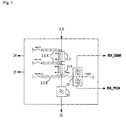
- FIG. 1 shows a known front-end circuit for a mobile radio device, that for two frequency ranges (here: GSM and PCN frequency, i.e. 900 and 1800 MHz) works.
- This front end circuit contains two couplers 11.3 and 11.4 on one Transmission path (TX path) from a power amplifier 2.X to an antenna 22, three ⁇ / 4 high-frequency lines are arranged 3.3.X before, between and after the branch off both couplers 11.3 and 11.4 from the transmission path and each have an RF switch (GSM_TX, PCN_TX, GSM_RX_TX).
- the front-end circuit also contains a filter arrangement 20 on the TX path in front of a circuit output. So is on the transmission path no switching element.
- the known front-end circuit contains on one Receive path another filter arrangement 21, wherein an RF switch (RXON) in front and another HF switch (TXONPA) are arranged after this filter arrangement 21.
- the filter arrangement 21 now separates the respective reception frequencies on two receive paths (RX_GSM, RX_PCN).
- the RXON switch is open for sending signals. To the All others are transmitting on the GSM operating frequency Switch closed, only the isolation switch for PCN operating frequencies TXONPA.
- the ⁇ / 4 radio frequency lines 3.3.X thus realize an idle and for the working frequency for double frequency, in GSM operation, a short circuit, whereby a very steep harmonic filter is realized.
- the ⁇ / 4 high-frequency lines are used for signal reception 3.3.X idles on the entry point of the RXON switch, which allow almost all of the energy is transferred to the RX paths.
- This known circuit has insertion loss of 0.9 dB on the TX-GSM path, 1.5 dB on the TX-PCN path and 1.5 to 2.5 dB for the RX paths.
- coupler outputs are forward and backward represented by reference numerals 24 and 25, their internal connection not shown for reasons of clarity is.
- Figure 2 shows a block diagram of the invention Front end circuit. Here you get with almost the same number the components to significantly improved electrical properties, than with the well-known single-deck front-end solution from FIG. 1.
- the circuit arrangement contains in this embodiment two changeover switches 23.1 and 23.2 (subcircuits), which have a crossover 19 and a subsequent low pass filter 18 to an antenna input / output 16 are merged.
- the upper subcircuit is on the GSM frequency (900 MHz), the lower one on the PCN frequency (1800 MHz).
- Each of the subcircuits 23.X contains on the TX path (transmission path) each a coupler 11.X, and before and after Coupler 11.X one high-frequency line 3.X.1 and 3.X.2 each are at the respective operating frequencies ⁇ / 4.
- the ⁇ / 4 radio frequency lines 3.X.1 each carry a switch (GSM_TX, PCN_TX), which is contacted to ground, the ⁇ / 4 high-frequency lines 3.X.2 end up with an idle or short circuit completed.
- reception paths each contain one RF switch (GSMRXON, PCNRXON), which closes when received and in the case of transmission, as shown here, is open.
- each individual subcircuit corresponds to 23.X. the functioning of those shown in Figure 1 single-front circuit. Because the way it works here due to fewer RF switches at the ends of the ⁇ / 4 high-frequency lines 3.X.X in the TX path and shorter lines (GSM by factor 2; PCN by factor 4) is reached the insertion loss of the TX paths compared to the single path Solution significantly reduced. Because the one-stop solution already an insertion loss that is lower by a factor of 2 as known two-tier solutions, the present invention is a big step forward in innovation.
- Figure 3 shows a schematic structure of the invention Front end circuit. Analogous to that shown in FIG. 2 Embodiment, the upper sub-circuit is on the GSM frequency of 900 MHz and the lower subcircuit the PCN frequency of 1800 MHz.
- the 900 MHz signal is at input 1.1 of a multi-stage Power amplifier 2.1 and from this on the branch 6.1 (GSM input of the front-end circuit) is given.
- a diode 4.1.1 is conductive, causing a short circuit a point 5 via a ⁇ / 4 high-frequency line 3.1.1 transformed to branch 6.1 in an idle state becomes.
- the ⁇ / 4 high-frequency line has exactly the same function 3.1.2.
- Both lines 3.1.1 and 3.1.2 influence the transmission of the 900 MHz signal almost completely Not.
- both lines 3.1.1 and 3.1.2 close a double over a ⁇ / 2 transformation of the short circuits Frequency short and therefore offer very good filtering of the first and all other odd harmonics.
- Coupler 11.1 couples, in the design shown, with a Coupling loop 7.1 a signal at point 8.1, for which of the Power amplifier 2.1 coming wave, and with the coupling loop 10.1, a signal reflected on the antenna.
- the two coupling loops 7.1 and 10.1 it is also sufficient a single one, the reflected signal being coupled out at point 9.1 and the wave sump (illustrated there as the tip of the triangle). In this case however, increased demands on downstream detectors regarding their input adjustment.
- Another Coupler variant or another control concept is to be found in the fact that only the incoming wave is coupled out becomes. In this case, the coupling loop 10.1 would be omitted and the coupling loop 7.1 would be unchanged.
- the diode 4.1.2 is blocked and the insulation diode 4.1.3 in the conductive state.
- the insulation diode 4.1.3 in the conductive state.
- another ⁇ / 4 high-frequency line can be used for these losses connected between the two diodes (not shown here).
- the short circuit of the Diode 4.1.3 in an idle state to terminate the diode 4.1.2 transforms which in addition to the insulation values the diode 4.1.2 the no-load characteristics at the junction 15.1 increased significantly.
- the signal to be transmitted comes from this branch 15.1 about network 17, which will be discussed in more detail below, low loss to antenna input / output 16.
- Sending and receiving signals on the PCN frequency can be viewed analogously to the GSM cases.
- the construction of the network 17 can be in several versions respectively. In the simplest case, a diplexer is used.
- Circuitry more complex, but possibly less expensive, is a discretely constructed crossover with subsequent Low pass filter as shown in Fig.2.
- Figure 4 shows a preferred embodiment of the invention Front end circuit, whereby for the construction of the Network 17 reached another very inexpensive solution becomes.
- two ⁇ / 4 high-frequency lines 3.4.1 and 3.4.2 are used, which are tuned to the PCN frequency are (PCN- ⁇ / 4 radio frequency lines) followed by one Low-pass filter 18.
- the low-pass filter 18 can also be used here omitted.
- the line 3.4.1 is between the branch point 15.1 and the antenna input / output 16 attached, the other line 3.4.2 connects the branch point 15.2 and the antenna input / output 16.
- the low-pass filter 18 is connected in series with antenna input / output 16.
- diode 4.2.2 and the diode 4.2.1 is switched through. Consequently, for the GSM frequency the short circuit of the diode 4.2.1 over the radio frequency line 3.2.1 and the PCN coupler 11.2 to an idle transformed and absorbed at the branch point 15.2 almost no energy there.
- the short circuit of the radio frequency line 3.2.2 is via the PCN- ⁇ / 4 radio frequency line 3.4.2 transformed into an idle in the antenna input / output 16. Consequently, most of the energy is between the branch point 15.1 and the antenna input / output 16 transported.
- RF switches can also be used instead of the PIN diodes such as using MesFETs.
- FIG. 5 shows an expansion of the front-end circuit 3 on three frequency channels. This concept is too expandable to other channels.
- Switching is enough for a triple band extension second pair of diodes 4.3.2 and 4.3.3 for selective decoupling for example the 1800 MHz and 1900 MHz receive signals to be connected in parallel with 4.2.2 and 4.2.3.
- the isolation diodes Remove 4.1.3, 4.2.3 and 4.3.3.
Landscapes
- Engineering & Computer Science (AREA)
- Computer Networks & Wireless Communication (AREA)
- Signal Processing (AREA)
- Transceivers (AREA)
Abstract
Description
- Figur 1:
- ein Blockschaltbild einer bekannten einzügigen Frontendschaltung für zwei Frequenzbereiche;
- Figur 2:
- ein Blockschaltbild der erfindungsgemäßen zweizügigen Frontendschaltung für zwei Frequenzbereiche;
- Figur 3:
- einen Aufbau der erfindungsgemäßen zweizügigen Frontendschaltung für zwei Frequenzbereiche;
- Figur 4:
- einen Aufbau eines bevorzugten Ausführungsbeispieles der erfindungsgemäßen zweizügigen Frontendschaltung für zwei Frequenzbereiche;
- Figur 5:
- einen Aufbau der erfindungsgemäßen zweizügigen Frontendschaltung für drei Frequenzbereiche.
- 1.X
- Eingang des Leistungsverstärkers 2.X
- 2.X
- Leistungsverstärker
- 3.X.X
- λ/4-Hochfrequenzleitung
- 4.X.X
- Diode
- 5
- Punkt
- 6.X
- Verzweigung
- 7.X
- Koppelschleife
- 8.X
- Punkt
- 9.X
- Punkt
- 10.X
- Koppelschleife
- 11.X
- Koppler
- 14.1
- GSM-RX-Ausgang
- 14.2
- PCN-RX-Ausgang
- 15.X
- Verzweigung
- 16
- Antenneneingang/-ausgang
- 17
- Netzwerk
- 18
- Tiefpaßfilter
- 19
- Frequenzweiche
- 20
- Filteranordnung
- 21
- Filteranordnung
- 22
- Antenne
- 23.X
- Umschalter
- 24
- Forward
- 25
- Backward
- 26.X
- Kopplerleitung
Claims (13)
- Frontendschaltung, insbesondere für Mobilfunk-Handgeräte mit mindestens einem Umschalter (23.X), der mindestens ein Mittel zum Auskoppeln von Sende- und Empfangssignalen, mindestens ein Mittel zur Frequenzselektion der Sende- und Empfangssignale und mindestens eine Hochfrequenzleitung mit einer elektrischen Länge von λ/4 aufweist, dadurch gekennzeichnet, daß der mindestens eine Umschalter (23.X) auf einer Leitung von einem Antenneneingang/-ausgang (16) zu einem Leistungsverstärker (2.X) einen Koppler (11.X) aufweist, wobei auf der Leitung zwischen Antenneneingang/-ausgang (16) und Koppler (11.X) eine λ/4-Hochfrequenzleitung (3.X.2), die direkt gegen Masse geschaltet ist, oder eine λ/2-Hochfrequenzleitung, die mit einem Leerlauf abgeschlossen ist, und zwischen dem Leistungsverstärker (2.X) und dem Koppler (11.X) mindestens eine λ/4-Hochfrequenzleitung (3.X.1) vorgesehen ist, die am Ende mit einem Kurzschluß oder Leerlauf abgeschlossen, und die in Reihe mit einem gegen Masse kontaktierten HF-Schalter (4.X.1) geschaltet ist, sowie zwischen der λ/4-Hochfrequenzleitung (3.X.2) oder der λ/2-Hochfrequenzleitung und dem Antenneneingang/-ausgang (16) eine Leitung zu einem RX-Ausgang (14.X) mit mindestens einem in Reihe geschalteten HF-Schalter (4.X.2) vorgesehen ist.
- Frontendschaltung gemäß dem voranstehenden Anspruch 1, dadurch gekennzeichnet, daß zwischen dem Koppler (11.X) und dem Leistungsverstärker (2.X) eine weitere zu der λ/4-Hochfrequenzleitung (3.X.1) parallel geschaltete λ/4-Hochfrequenzleitung vorgesehen ist, die am Ende direkt gegen Masse kontaktiert ist.
- Frontendschaltung gemäß dem voranstehenden Anspruch 2, dadurch gekennzeichnet, daß zwischen dem HF-Schalter (4.X.2) und dem RX-Ausgang (14.X) eine Leitung abzweigt, die einen gegen Masse kontaktierten HF-Schalter (4.X.3) aufweist.
- Frontendschaltung gemäß dem voranstehenden Anspruch 3, dadurch gekennzeichnet, daß zwischen dem HF-Schalter (4.X.2) und dem gegen Masse kontaktierten HF-Schalter (4.X.3) eine weitere λ/4-Hochfrequenzleitung vorgesehen ist.
- Frontendschaltung gemäß einem der voranstehenden Ansprüche 1 bis 4, dadurch gekennzeichnet, daß der mindestens eine HF-Schalter (4.X.X) als PIN-Diode und/oder HEMT und/oder MesFET ausgebildet ist.
- Frontendschaltung gemäß einem der voranstehenden Ansprüche 1 bis 5, dadurch gekennzeichnet, daß mindestens ein weiterer Umschalter (23.X), vorzugsweise für eine andere Frequenz, vorgesehen ist.
- Frontendschaltung gemäß dem voranstehenden Anspruch 6, dadurch gekennzeichnet, daß die mindestens zwei Umschalter (23.X) über ein Netzwerk (17) auf den Antenneneingang/-ausgang (16) zusammenlaufen.
- Frontendschaltung gemäß dem voranstehenden Anspruch 7, dadurch gekennzeichnet, daß das Netzwerk (17) einen Diplexer aufweist.
- Schaltungsanordung gemäß einem der voranstehenden Ansprüche 7 bis 8, dadurch gekennzeichnet, daß das Netzwerk (17) eine Frequenzweiche (19) mit anschließendem Tiefpaßfilter (18) aufweist.
- Frontendschaltung gemäß dem voranstehenden Anspruch 9, dadurch gekennzeichnet, daß die Frequenzweiche (19) mindestens einen Breitpaßfilter und/oder mindestens einen Hochpaßfilter und/oder mindestens einen Tiefpaßfilter (18) aufweist.
- Schaltungsanordung gemäß einem der voranstehenden Ansprüche 7 bis 10, dadurch gekennzeichnet, daß das Netzwerk (17) mindestens zwei λ/4-Hochfrequenzleitungen (3.4.X), deren Längen auf mindestens eine der zu sendenden/empfangenden Frequenzen abgestimmt sind, aufweist.
- Frontendschaltung gemäß dem voranstehenden Anspruch 11, dadurch gekennzeichnet, daß den λ/4-Hochfrequenzleitungen (3.4.X) ein Tiefpaßfilter (18) nachgestellt ist.
- Frontendschaltung gemäß einem der voranstehenden Ansprüche1 bis 12, dadurch gekennzeichnet, daß zur Abstimmung mindestens eines Umschalters (23.X) auf eine benachbarte Frequenz mindestens ein weiterer HF-Schalter (4.3.X) vorgesehen ist, der parallel zu dem HF-Schalter (4.X.2) geschaltet wird.
Priority Applications (2)
| Application Number | Priority Date | Filing Date | Title |
|---|---|---|---|
| DE50014116T DE50014116D1 (de) | 2000-04-07 | 2000-04-07 | Frontendschaltung für Mobilfunk-Handgeräte |
| EP00107571A EP1143629B1 (de) | 2000-04-07 | 2000-04-07 | Frontendschaltung für Mobilfunk-Handgeräte |
Applications Claiming Priority (1)
| Application Number | Priority Date | Filing Date | Title |
|---|---|---|---|
| EP00107571A EP1143629B1 (de) | 2000-04-07 | 2000-04-07 | Frontendschaltung für Mobilfunk-Handgeräte |
Publications (2)
| Publication Number | Publication Date |
|---|---|
| EP1143629A1 true EP1143629A1 (de) | 2001-10-10 |
| EP1143629B1 EP1143629B1 (de) | 2007-02-28 |
Family
ID=8168401
Family Applications (1)
| Application Number | Title | Priority Date | Filing Date |
|---|---|---|---|
| EP00107571A Expired - Lifetime EP1143629B1 (de) | 2000-04-07 | 2000-04-07 | Frontendschaltung für Mobilfunk-Handgeräte |
Country Status (2)
| Country | Link |
|---|---|
| EP (1) | EP1143629B1 (de) |
| DE (1) | DE50014116D1 (de) |
Cited By (1)
| Publication number | Priority date | Publication date | Assignee | Title |
|---|---|---|---|---|
| EP2019494A1 (de) | 2004-11-25 | 2009-01-28 | Murata Manufacturing Co. Ltd. | Hochfrequenzschaltmodul |
Citations (5)
| Publication number | Priority date | Publication date | Assignee | Title |
|---|---|---|---|---|
| JPS60174534A (ja) * | 1984-02-20 | 1985-09-07 | Toyo Commun Equip Co Ltd | アンテナ・スイツチ回路 |
| US5109205A (en) * | 1990-11-08 | 1992-04-28 | Honeywell Inc. | Millimeter wave microstrip shunt-mounted pin diode switch with particular bias means |
| US5486797A (en) * | 1994-08-04 | 1996-01-23 | Uniden Corporation | Integrated port selection circuit for high frequency signal |
| JPH09270732A (ja) * | 1996-04-02 | 1997-10-14 | Kokusai Electric Co Ltd | 方向性結合器付きアンテナ共用器 |
| US5778306A (en) * | 1996-11-08 | 1998-07-07 | Motorola Inc. | Low loss high frequency transmitting/receiving switching module |
-
2000
- 2000-04-07 EP EP00107571A patent/EP1143629B1/de not_active Expired - Lifetime
- 2000-04-07 DE DE50014116T patent/DE50014116D1/de not_active Expired - Lifetime
Patent Citations (5)
| Publication number | Priority date | Publication date | Assignee | Title |
|---|---|---|---|---|
| JPS60174534A (ja) * | 1984-02-20 | 1985-09-07 | Toyo Commun Equip Co Ltd | アンテナ・スイツチ回路 |
| US5109205A (en) * | 1990-11-08 | 1992-04-28 | Honeywell Inc. | Millimeter wave microstrip shunt-mounted pin diode switch with particular bias means |
| US5486797A (en) * | 1994-08-04 | 1996-01-23 | Uniden Corporation | Integrated port selection circuit for high frequency signal |
| JPH09270732A (ja) * | 1996-04-02 | 1997-10-14 | Kokusai Electric Co Ltd | 方向性結合器付きアンテナ共用器 |
| US5778306A (en) * | 1996-11-08 | 1998-07-07 | Motorola Inc. | Low loss high frequency transmitting/receiving switching module |
Non-Patent Citations (2)
| Title |
|---|
| PATENT ABSTRACTS OF JAPAN vol. 010, no. 011 (E - 374) 17 January 1986 (1986-01-17) * |
| PATENT ABSTRACTS OF JAPAN vol. 1998, no. 02 30 January 1998 (1998-01-30) * |
Cited By (2)
| Publication number | Priority date | Publication date | Assignee | Title |
|---|---|---|---|---|
| EP2019494A1 (de) | 2004-11-25 | 2009-01-28 | Murata Manufacturing Co. Ltd. | Hochfrequenzschaltmodul |
| US7756488B2 (en) | 2004-11-25 | 2010-07-13 | Murata Manufacturing Co., Ltd | High-frequency switch module |
Also Published As
| Publication number | Publication date |
|---|---|
| EP1143629B1 (de) | 2007-02-28 |
| DE50014116D1 (de) | 2007-04-12 |
Similar Documents
| Publication | Publication Date | Title |
|---|---|---|
| DE112009005411B4 (de) | Leistungsverstärkerschaltung und Anpassungsschaltung | |
| DE60116676T2 (de) | Mehrband-Transformationsstufe für eine Mehrband-HF-Umschaltvorrichtung | |
| DE69835937T2 (de) | Zweifrequenzschalter, anordnung mit gemeinsamer zweifrequenzantenne und mobile zweifrequenz-funkübertragungsausrüstung damit | |
| DE102010046677B4 (de) | Schaltungsanordnung | |
| DE69421948T2 (de) | Integrierter Frequenzumsetzer mit Spiegelfrequenz-Unterdrückung | |
| DE69812120T2 (de) | Doppelbandiger leistungsverstärker mit zwei betriebsarten | |
| DE68910403T2 (de) | Übertragungsleitungsschalter. | |
| DE19823049C2 (de) | Leistungsverstärker-Ausgangsschaltung zur Unterdrückung von Oberschwingungen für eine Mobilfunkeinheit mit Doppelbandbetrieb und Verfahren zum Betreiben derselben | |
| DE10053205B4 (de) | Kombinierte Frontendschaltung für drahtlose Übertragungssysteme | |
| DE69529559T2 (de) | Halbduplexfunkgerät mit niedriger Dämpfung des Sendesignals | |
| DE69929968T2 (de) | Antennenschalter | |
| DE69431547T2 (de) | Antennenschalter | |
| DE60315646T2 (de) | Antennenumschaltungsvorrichtung | |
| DE102011012927B4 (de) | Verstärkermodul | |
| DE19853484A1 (de) | Hochfrequente Schalteinrichtung | |
| DE3522564A1 (de) | Sende-/empfangsschalter | |
| WO2000018026A1 (de) | Mehrband-antennenschalter | |
| DE102008012984A1 (de) | Mischerschaltung und Radar-Transceiver | |
| DE10200048A1 (de) | Verbindung der Sende- und Empfangseinrichtungen von Multiband-/Multimode-Funkgeräten mit einer oder mehreren Antennen | |
| DE19954257A1 (de) | Mischer für mehrere Bänder für lokalen Oszillator | |
| EP1168500A2 (de) | Antennenumschalter für Sende-Empfangseinheiten in einer Mobilstation | |
| DE102007005676A1 (de) | Umschalt-Schaltung sowie Eingangsmodul und Mobiltelefon mit dieser Schaltung | |
| DE2649233C3 (de) | Frequenzverknüpfungsschaltung | |
| EP1143629B1 (de) | Frontendschaltung für Mobilfunk-Handgeräte | |
| DE102005037877A1 (de) | Diodenmischer |
Legal Events
| Date | Code | Title | Description |
|---|---|---|---|
| PUAI | Public reference made under article 153(3) epc to a published international application that has entered the european phase |
Free format text: ORIGINAL CODE: 0009012 |
|
| AK | Designated contracting states |
Kind code of ref document: A1 Designated state(s): AT BE CH CY DE DK ES FI FR GB GR IE IT LI LU MC NL PT SE Kind code of ref document: A1 Designated state(s): DE FI FR GB NL |
|
| AX | Request for extension of the european patent |
Free format text: AL;LT;LV;MK;RO;SI |
|
| 17P | Request for examination filed |
Effective date: 20020402 |
|
| AKX | Designation fees paid |
Free format text: DE FI FR GB NL |
|
| GRAP | Despatch of communication of intention to grant a patent |
Free format text: ORIGINAL CODE: EPIDOSNIGR1 |
|
| GRAS | Grant fee paid |
Free format text: ORIGINAL CODE: EPIDOSNIGR3 |
|
| GRAA | (expected) grant |
Free format text: ORIGINAL CODE: 0009210 |
|
| AK | Designated contracting states |
Kind code of ref document: B1 Designated state(s): DE FI FR GB NL |
|
| PG25 | Lapsed in a contracting state [announced via postgrant information from national office to epo] |
Ref country code: FI Free format text: LAPSE BECAUSE OF FAILURE TO SUBMIT A TRANSLATION OF THE DESCRIPTION OR TO PAY THE FEE WITHIN THE PRESCRIBED TIME-LIMIT Effective date: 20070228 Ref country code: NL Free format text: LAPSE BECAUSE OF FAILURE TO SUBMIT A TRANSLATION OF THE DESCRIPTION OR TO PAY THE FEE WITHIN THE PRESCRIBED TIME-LIMIT Effective date: 20070228 |
|
| REG | Reference to a national code |
Ref country code: GB Ref legal event code: FG4D Free format text: NOT ENGLISH |
|
| REF | Corresponds to: |
Ref document number: 50014116 Country of ref document: DE Date of ref document: 20070412 Kind code of ref document: P |
|
| NLV1 | Nl: lapsed or annulled due to failure to fulfill the requirements of art. 29p and 29m of the patents act | ||
| GBV | Gb: ep patent (uk) treated as always having been void in accordance with gb section 77(7)/1977 [no translation filed] |
Effective date: 20070228 |
|
| EN | Fr: translation not filed | ||
| PG25 | Lapsed in a contracting state [announced via postgrant information from national office to epo] |
Ref country code: GB Free format text: LAPSE BECAUSE OF FAILURE TO SUBMIT A TRANSLATION OF THE DESCRIPTION OR TO PAY THE FEE WITHIN THE PRESCRIBED TIME-LIMIT Effective date: 20070228 |
|
| PLBE | No opposition filed within time limit |
Free format text: ORIGINAL CODE: 0009261 |
|
| STAA | Information on the status of an ep patent application or granted ep patent |
Free format text: STATUS: NO OPPOSITION FILED WITHIN TIME LIMIT |
|
| 26N | No opposition filed |
Effective date: 20071129 |
|
| PG25 | Lapsed in a contracting state [announced via postgrant information from national office to epo] |
Ref country code: FR Free format text: LAPSE BECAUSE OF FAILURE TO SUBMIT A TRANSLATION OF THE DESCRIPTION OR TO PAY THE FEE WITHIN THE PRESCRIBED TIME-LIMIT Effective date: 20071019 |
|
| PG25 | Lapsed in a contracting state [announced via postgrant information from national office to epo] |
Ref country code: FR Free format text: LAPSE BECAUSE OF FAILURE TO SUBMIT A TRANSLATION OF THE DESCRIPTION OR TO PAY THE FEE WITHIN THE PRESCRIBED TIME-LIMIT Effective date: 20070228 |
|
| PGFP | Annual fee paid to national office [announced via postgrant information from national office to epo] |
Ref country code: DE Payment date: 20170613 Year of fee payment: 18 |
|
| REG | Reference to a national code |
Ref country code: DE Ref legal event code: R119 Ref document number: 50014116 Country of ref document: DE |
|
| PG25 | Lapsed in a contracting state [announced via postgrant information from national office to epo] |
Ref country code: DE Free format text: LAPSE BECAUSE OF NON-PAYMENT OF DUE FEES Effective date: 20181101 |