EP1139355A1 - Electronic device of ceramic - Google Patents
Electronic device of ceramic Download PDFInfo
- Publication number
- EP1139355A1 EP1139355A1 EP00961152A EP00961152A EP1139355A1 EP 1139355 A1 EP1139355 A1 EP 1139355A1 EP 00961152 A EP00961152 A EP 00961152A EP 00961152 A EP00961152 A EP 00961152A EP 1139355 A1 EP1139355 A1 EP 1139355A1
- Authority
- EP
- European Patent Office
- Prior art keywords
- ceramic
- ceramic sheet
- electronic components
- conductive layer
- manufacturing
- Prior art date
- Legal status (The legal status is an assumption and is not a legal conclusion. Google has not performed a legal analysis and makes no representation as to the accuracy of the status listed.)
- Withdrawn
Links
Images

Classifications
-
- H—ELECTRICITY
- H10—SEMICONDUCTOR DEVICES; ELECTRIC SOLID-STATE DEVICES NOT OTHERWISE PROVIDED FOR
- H10W—GENERIC PACKAGES, INTERCONNECTIONS, CONNECTORS OR OTHER CONSTRUCTIONAL DETAILS OF DEVICES COVERED BY CLASS H10
- H10W70/00—Package substrates; Interposers; Redistribution layers [RDL]
- H10W70/01—Manufacture or treatment
- H10W70/05—Manufacture or treatment of insulating or insulated package substrates, or of interposers, or of redistribution layers
-
- H—ELECTRICITY
- H01—ELECTRIC ELEMENTS
- H01G—CAPACITORS; CAPACITORS, RECTIFIERS, DETECTORS, SWITCHING DEVICES, LIGHT-SENSITIVE OR TEMPERATURE-SENSITIVE DEVICES OF THE ELECTROLYTIC TYPE
- H01G4/00—Fixed capacitors; Processes of their manufacture
- H01G4/002—Details
- H01G4/018—Dielectrics
- H01G4/20—Dielectrics using combinations of dielectrics from more than one of groups H01G4/02 - H01G4/06
- H01G4/206—Dielectrics using combinations of dielectrics from more than one of groups H01G4/02 - H01G4/06 inorganic and synthetic material
-
- H—ELECTRICITY
- H01—ELECTRIC ELEMENTS
- H01G—CAPACITORS; CAPACITORS, RECTIFIERS, DETECTORS, SWITCHING DEVICES, LIGHT-SENSITIVE OR TEMPERATURE-SENSITIVE DEVICES OF THE ELECTROLYTIC TYPE
- H01G4/00—Fixed capacitors; Processes of their manufacture
- H01G4/30—Stacked capacitors
-
- H—ELECTRICITY
- H05—ELECTRIC TECHNIQUES NOT OTHERWISE PROVIDED FOR
- H05K—PRINTED CIRCUITS; CASINGS OR CONSTRUCTIONAL DETAILS OF ELECTRIC APPARATUS; MANUFACTURE OF ASSEMBLAGES OF ELECTRICAL COMPONENTS
- H05K3/00—Apparatus or processes for manufacturing printed circuits
- H05K3/10—Apparatus or processes for manufacturing printed circuits in which conductive material is applied to the insulating support in such a manner as to form the desired conductive pattern
- H05K3/12—Apparatus or processes for manufacturing printed circuits in which conductive material is applied to the insulating support in such a manner as to form the desired conductive pattern using thick film techniques, e.g. printing techniques to apply the conductive material or similar techniques for applying conductive paste or ink patterns
- H05K3/1283—After-treatment of the printed patterns, e.g. sintering or curing methods
-
- H—ELECTRICITY
- H05—ELECTRIC TECHNIQUES NOT OTHERWISE PROVIDED FOR
- H05K—PRINTED CIRCUITS; CASINGS OR CONSTRUCTIONAL DETAILS OF ELECTRIC APPARATUS; MANUFACTURE OF ASSEMBLAGES OF ELECTRICAL COMPONENTS
- H05K3/00—Apparatus or processes for manufacturing printed circuits
- H05K3/46—Manufacturing multilayer circuits
- H05K3/4611—Manufacturing multilayer circuits by laminating two or more circuit boards
- H05K3/4626—Manufacturing multilayer circuits by laminating two or more circuit boards characterised by the insulating layers or materials
- H05K3/4629—Manufacturing multilayer circuits by laminating two or more circuit boards characterised by the insulating layers or materials laminating inorganic sheets comprising printed circuits, e.g. green ceramic sheets
-
- H—ELECTRICITY
- H10—SEMICONDUCTOR DEVICES; ELECTRIC SOLID-STATE DEVICES NOT OTHERWISE PROVIDED FOR
- H10W—GENERIC PACKAGES, INTERCONNECTIONS, CONNECTORS OR OTHER CONSTRUCTIONAL DETAILS OF DEVICES COVERED BY CLASS H10
- H10W99/00—Subject matter not provided for in other groups of this subclass
-
- H—ELECTRICITY
- H05—ELECTRIC TECHNIQUES NOT OTHERWISE PROVIDED FOR
- H05K—PRINTED CIRCUITS; CASINGS OR CONSTRUCTIONAL DETAILS OF ELECTRIC APPARATUS; MANUFACTURE OF ASSEMBLAGES OF ELECTRICAL COMPONENTS
- H05K1/00—Printed circuits
- H05K1/02—Details
- H05K1/03—Use of materials for the substrate
- H05K1/0306—Inorganic insulating substrates, e.g. ceramic, glass
-
- H—ELECTRICITY
- H05—ELECTRIC TECHNIQUES NOT OTHERWISE PROVIDED FOR
- H05K—PRINTED CIRCUITS; CASINGS OR CONSTRUCTIONAL DETAILS OF ELECTRIC APPARATUS; MANUFACTURE OF ASSEMBLAGES OF ELECTRICAL COMPONENTS
- H05K2203/00—Indexing scheme relating to apparatus or processes for manufacturing printed circuits covered by H05K3/00
- H05K2203/01—Tools for processing; Objects used during processing
- H05K2203/0104—Tools for processing; Objects used during processing for patterning or coating
- H05K2203/0143—Using a roller; Specific shape thereof; Providing locally adhesive portions thereon
-
- H—ELECTRICITY
- H05—ELECTRIC TECHNIQUES NOT OTHERWISE PROVIDED FOR
- H05K—PRINTED CIRCUITS; CASINGS OR CONSTRUCTIONAL DETAILS OF ELECTRIC APPARATUS; MANUFACTURE OF ASSEMBLAGES OF ELECTRICAL COMPONENTS
- H05K2203/00—Indexing scheme relating to apparatus or processes for manufacturing printed circuits covered by H05K3/00
- H05K2203/02—Details related to mechanical or acoustic processing, e.g. drilling, punching, cutting, using ultrasound
- H05K2203/0278—Flat pressure, e.g. for connecting terminals with anisotropic conductive adhesive
-
- H—ELECTRICITY
- H05—ELECTRIC TECHNIQUES NOT OTHERWISE PROVIDED FOR
- H05K—PRINTED CIRCUITS; CASINGS OR CONSTRUCTIONAL DETAILS OF ELECTRIC APPARATUS; MANUFACTURE OF ASSEMBLAGES OF ELECTRICAL COMPONENTS
- H05K3/00—Apparatus or processes for manufacturing printed circuits
- H05K3/0011—Working of insulating substrates or insulating layers
Definitions
- the present invention relates to a method of manufacturing ceramic electronic components such as multilayer ceramic capacitors and the like.
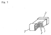
- Fig. 7 is a partially cut-away perspective view of a typical multilayer ceramic capacitor comprising a ceramic dielectric layer 1, a conductive layer 2 and a pair of external electrodes 3, in which an end of each respective conductive layer 2 is alternately connected with one of the pair of external electrodes 3 at the two side of the ceramic dielectric layer 1.
- a ceramic sheet eventually constituting the ceramic dielectric layer 1 is prepared by mixing an organic material to a powder mainly composed of barium titanate ,and a metallic paste is applied thereon in a required pattern by a printing method to form the conductive layer 2. Then, a plurality of the ceramic sheets, each applied with the conductive layer 2 thereon, are superimposed one over another in such a way that any two adjoining conductive layers 2 are located opposite to each other with the ceramic sheet sandwiched therebetween, thus obtaining a laminate. The laminate is fired thereafter and a pair of the external electrodes 3 are formed on both side where the conductive layer 2 is exposed.
- a ceramic sheet for a multilayer ceramic capacitor is made thinner and thinner in order to gain higher capacitance in said capacitor, thereby causing a problem of short-circuiting between adjoining two electrodes because of the metal constituent that has penetrated into the ceramic sheet.
- the object of the present invention is to provide a method of manufacturing ceramic electronic component with less failures due to said short-circuiting.
- the method of manufacturing ceramic electronic components according to the present invention is characterized in that the porosity of a ceramic sheet is first reduced and then a conductive layer is formed on the surface thereof, thereby allowing a metallic constituent to be prevented from penetrating into the ceramic sheet with resulting prevention of short-circuiting failure that may otherwise occur between the conductive layers.
- a method of manufacturing ceramic electronic components in a first exemplary embodiment of the present invention comprises:
- a method of manufacturing said components in a second exemplary embodiment of the present invention is the method of said components according to the first exemplary embodiment, in which the porosity of the ceramic sheet before a reduction in porosity after the first step is 50 % or more, thereby allowing a ceramic electronic component free of short-circuiting failures to be realized.
- a method of manufacturing said components in a third exemplary embodiment of the present invention is the method of said components according to the first exemplary embodiment, in which the ceramic sheet contains at least a ceramic constituent and polyethylene at the first step, thereby achieving a great effect in reducing short-circuiting failures, because of a high level of porosity in the ceramic sheet containing polyethylene,compared with other organic materials.
- a method of manufacturing ceramic electronic components in a fourth exemplary embodiment of the present invention is the method of said components according to the first exemplary embodiment, in which the porosity of a ceramic sheet at the first step is less than 50 %, thereby allowing a metallic constituent to be prevented from penetrating into the ceramic sheet.
- a method of manufacturing ceramic electronic components in a fifth exemplary embodiment of the present invention is the method of said components according to the first exemplary embodiment, in which the pressing force applied to the ceramic sheet at the first step is made less than the pressing force as applied in forming the laminate at the third step, thereby allowing a sufficiently uniform pressing force to be applied to the entire laminate in both areas, with and without a conductive layer at the third step, resulting in a realization of an electronic component that has little structural defect due to failures in adhesion between the ceramic sheets.
- a method of manufacturing ceramic electronic components in a sixth exemplary embodiment of the present invention is the method of said components according to the first exemplary embodiment, in which the ceramic sheet is heated while a pressing force being applied thereto at the first step, thereby allowing the fluidity of an organic material to be enhanced by the application of heat with a resulting quick reduction in porosity of the ceramic sheet.
- a method of manufacturing ceramic electronic components in a seventh exemplary embodiment of the present invention is the method of said components according to the sixth exemplary embodiment, in which the ceramic sheet is heated at the temperature between the glass transition point and the melting point of at least one organic material contained in the ceramic sheet , thereby allowing the fluidity of organic materials to be enhanced by the application of heat with a resulting quick reduction in porosity of the ceramic sheet.
- a method of manufacturing ceramic electronic components in an eighth exemplary embodiment of the present invention comprises:
- a method of manufacturing ceramic electronic components in a ninth exemplary embodiment of the present invention is the method of said components according to the eighth exemplary embodiment, in which the porosity of the ceramic sheet before the first step is 50 % or more, thereby allowing a said component free of short-circuiting failures to be realized.
- a method of manufacturing ceramic electronic components in a tenth exemplary embodiment of the present invention is the method of said components according to the eighth exemplary embodiment, in which the ceramic sheet is prepared so as to contain at least a ceramic powder and polyethylene at the first step, thereby achieving a great effect in reducing short-circuiting failures.
- the rate of volumetric shrinkage of the ceramic sheet after the application of a pressing force thereto is made uniform in those composition because of the high level in porosity of the ceramic sheet before applying the pressing force thereto and allowing a further reduction in porosity of the ceramic ceramic sheet to be achieved.
- a method of manufacturing ceramic electronic components in an eleventh exemplary embodiment of the present invention is the method of said components according to the eighth exemplary embodiment, in which the porosity of the ceramic sheet after the first step is less than 50 %, thereby allowing the metallic constituent to be prevented from penetrating into the ceramic sheet.
- a method of manufacturing ceramic electronic components in a twelfth exemplary embodiment of the present invention is the method of said components according to the eighth exemplary embodiment, in which the pressing force applied to the ceramic sheet at the first step is made less than the pressing force as applied in forming the laminate at the third step, thereby allowing a sufficiently uniform pressing force to be applied to the entire laminate in both region with and without the conductive layer at the third step, resulting in a realization of an electronic component that has little structural defect due to failures in adhesion between the ceramic sheets.
- a method of manufacturing ceramic electronic components in a thirteenth exemplary embodiment of the present invention is the method of said components according to the eighth exemplary embodiment, in which the ceramic sheet is heated while a pressing force being applied thereto at the first step, thereby allowing the fluidity of the organic material to be enhanced by the heat application with a resulting quick reduction in porosity of the ceramic sheet.
- a method of manufacturing ceramic electronic components in a fourteenth exemplary embodiment of the present invention is the method of said components according to the eighth exemplary embodiment, in which the ceramic sheet is heated at the temperature between the glass transition point and the melting point of at least one organic material contained in the ceramic sheet, thereby allowing the fluidity of organic materials to be enhance by the heat application with a resulting quick reduction in porosity of the ceramic sheet.
- a method of manufacturing ceramic electronic components in a fifteenth exemplary embodiment of the present invention is the method of said components according to the eighth exemplary embodiment, in which the amount of an organic constituent in the conductive layer before lamination process is from 5 wt % to 15 wt % against 100 wt % of the metallic constituent at the third step, thereby allowing the sufficient adhesion between the conductor and the ceramic sheet to be realized, resulting in obtaining a ceramic component that has little structural defect.
- a method of manufacturing ceramic electronic components in a sixteenth exemplary embodiment of the present invention is the method of said components according to the eighth exemplary embodiment, with additional step of applying a pressing force to the conductive layer in the thickness direction thereof placed between the second step and the third step, thereby allowing the microscopic asperities on the surface of the conductor layer to be reduced and contributing further to the prevention of short-circuiting failures.
- a method of manufacturing ceramic electronic components in a seventeenth exemplary embodiment of the present invention comprises:
- a method of manufacturing ceramic electronic components in an eighteenth exemplary embodiment is the method according to the seventeenth exemplary embodiment, in which the porosity of the ceramic sheet is less than 50 %, thereby allowing a metallic constituent to be prevented from penetrating the ceramic sheet.
- a method of manufacturing ceramic electronic components in a nineteenth exemplary embodiment is the method according to the seventeenth exemplary embodiment, in which, after the conductive layer formed on a base film is superimposed on the ceramic sheet at the first step, a step of peeling off the base film and a step of superimposing the ceramic sheet on the conductive layer are repeated one after another, thereby allowing the solvent constituent in the conductive layer to be reduced when compared with the case where the conductive layer is formed directly on the ceramic sheet with a resulting contribution to preventing the metallic constituent from penetrating into the ceramic sheet.
- a method of manufacturing ceramic electronic components in a twentieth exemplary embodiment of the present invention is the method according to the nineteenth exemplary embodiment, with an additional step of applying a pressing force to the conductive layer on the base film in the thickness direction before the conductive layer is superimposed on the ceramic sheet, thereby allowing the microscopic asperities on the surface of the conductor layer to be reduced ,with a resulting contribution to preventing the metallic constituent from penetrating into the ceramic sheet.
- a method of manufacturing ceramic electronic components in a twenty first exemplary embodiment of the present invention is the method of said components according to the seventeenth exemplary embodiment, in which the conductive layer is deposited by the thin film process at the first step, in this case a metallic film is grown into a plate-like shape on the ceramic sheet, thereby allowing the metallic constituent to be prevented from penetrating into the sheet.
- a methods of manufacturing ceramic electronic components in a twenty second exemplary embodiment to a twenty fourth exemplary embodiment of the present invention comprise a step of preparing a laminate by stacking ceramic sheets, each containing an organic material and a ceramic powder, and conductive layers one over another alternately, in which the ceramic sheet is formed with the organic material arranged horizontally in a mesh-like structure and arranged at random in the thickness direction , thereby having the particles of the ceramic powder absorbed in the meshes of the organic material.
- the ceramic particles are also arranged at random, each presenting a mesh-like structure.
- a ceramic electronic component characterized as having a structure formed by stacking the ceramic layers, each having mesh-like structures of ceramic particles arranged at random, and the conductive layers one over another alternately shows a reduced number of short-circuiting pathes.
- a ceramic sheet 10a of 10 ⁇ m thick is prepared by the use of a cerainic powder composing barium titanate as major component and polyethylene of an average molecular weight of 400,000 or more .
- the porosity of this ceramic sheet 10a usually is around 65 %.
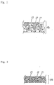
- Fig. 1 is a partially enlarged cross-sectional view of the ceramic sheet 10a, showing that ceramic particles 11 are sporadically located among the fibers of polyethylene 12 with a lot of voids 13 formed therein.
- the polyethylene 12 is formed in a mesh-like structure extending horizontally and at random in the thickness direction, where the ceramic particles 11 are absorbed in the meshes, thereby eventually having the ceramic particles 11 also arranged in a mesh-like structure extending horizontally and at random vertically.
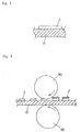
- the ceramic sheet 10a is passed through between rollers 14a and 14b, each provided with a smooth surfaceAt this time, the roller 14a and roller 14b are, respectively, rotating in a direction opposite to each other, and the ceramic sheet 10a is applied with a pressing force in the direction of thickness thereof and also heated.
- the porosity thereof is allowed to be reduced easily.
- the fluidity of polyethylene 12 is increased at the process of a pressing force application, resulting in having the air inside of said sheet 10a discharged outside and also become the density of the ceramic particles 11 higher.
- the heat treatment is carried out at the temperature between a glass transition point of polyethylene and the melting point thereof. More specifically, the optimum heating temperature ranges from 60 °C to 150 °C
- test ceramic sheets 10b are prepared in four kinds of porosity, i.e., 40 %, 30 %, 20 % and 10 %.
- Fig. 2 is a partially enlarged cross-sectional view of the ceramic sheet 10b after the application of a pressing force and heat treatment. As shown in Fig. 2, the region occupied by voids 13 are reduced dramatically. Moreover, the fibers of polyethylene 12 are formed in a mesh-like structure extending horizontally and at random in the thickness direction with the ceramic particles 11 absorbed in the meshes formed of polyethylene fibers.
- a metallic paste is prepared by the use of nickel powder as a metallic constituent, a binder formed of ethylcellulose, acrylic resin and butyral resin, benzylbutylphtalate as a plasticizer, and an aliphatic compound or an aromatic compound as a solvent, and the metallic paste is printed on the ceramic sheet 10b, where the porosity has been reduced already, in a desired pattern and then dried, thereby realizing a conductive layer of 2 to 2.5 ⁇ m thick.
- dummy layers are prepared by stacking one over another a plurality of ceramic sheets 10b, without conductive layer 2 and then a required number of a ceramic sheet 10b with a conductive layer 2 formed thereon are superimposed on the dummy layers, and further dummy layers are stacked thereon, thereby realizing a provisional laminate. At this time, it does not matter whether the ceramic sheet 10a having the porosity not reduced or having the porosity reduced as the dummy sheets.
- the use of the dummy sheet 10a having the porosity not reduced is preferable, because the unbalance of the pressing force caused by a difference in level existing between the region with the conductive layer 2 and the region without conductive layer 2 is relieved.
- the ceramic sheets 10b of 150 layer with the conductive layers 2 formed thereon are used and the dummy sheets 10a without porosity reduction are used.
- the laminate After a pressing force is applied to the entire provisional laminate, the laminate is cut into a desired shape, degreased and then fired.
- the degreasing process is preferably to be performed by the steps of eliminating the plasticizer from the laminate while the temperature of the laminate being elevated and then eliminating the binder with the temperature of the laminate further elevated, because a new chemical compound is created from the plasticizer and binder upon quick heating the laminate at a dash in order to eliminate the plasticizer and binder at the same time, and is left in the laminate even after the degreasing process.
- said chemical compound is burned and splashed out of the laminate and cause structural defects in the laminate such as delamination and the like, resulting in the increased number of short-circuiting failures.
- it is required to prevent the nickel contained in the conductive layer 2 from being excessively oxidized, when the steps of degreasing and firing are performed in succession.
- the ceramic dielectric layer 1 composing barium titanate as a major component and the conductive layer 2 composing nickel as a major component are combined together by sintering.
- the external electrodes 3 composing of copper and the like are formed, on both end surfaces of the sintered product where the conductive layer 2 exposed at the end surfaces by baking or plating process, thereby obtaining a maultilayer ceramic capacitor as shown in Fig. 7 .
- the prior art capacitor 1 is prepared according to the conventional method applied the conductive layer 2 on a ceramic sheet 10a with no reduction in porosity. As shown in Table 1, the fraction defectives due to short-circuiting are greatly reduced with the capacitors in the present exemplary embodiment when compared with the capacitor 1 according to the prior art. As the result of analyzing the cross-section of a multilayer ceramic capacitor with short circuiting failure, it is observed that the metallic path goes through the dielectric layers 1. Therefore, the present exemplary embodiment allows the metallic constituent in the conductive layer 2 to be prevented from penetrating into the ceramic sheet 10b, thereby greatly reducing the number of short circuits failures and enabling the remarkable improvement in manufacturing yields of multilayer ceramic capacitors.
- the high polymer polyethylene used as the binder is bulky when compared with polyvynil butyral resin and acrylic resin, making the ceramic sheet 10a rather high in porosity. Therefore, particularly in this case, reduction process of the porosity before forming the conductive layers 2 as proposed in the present invention are extremely effective in reducing failures due to short-circuiting.
- a conductive layer 2 is formed by printing directly a metallic paste on the ceramic sheet 10a that has already been reduced in porosity, but in the present exemplary embodiment a conductive layer 2 formed in advance on a base film 15 made of polyethyleneterephtlate and the like is transferred onto the ceramic sheet 10a.
- the porosity of the ceramic sheet 10a is reduced in the same way as in the first exemplary embodiment, and four different ceramic sheets 10a having 40%, 30%, 20% and 10%,, in porosity are prepared.
- a conductive layer 2 is formed on the base film 15 by printing a metallic paste thereon in a desired pattern and thendrying the paste. Thereafter, almost all the solvent contained in said layer 2 is released, thereby allowing the surface of theconductive layer 2 to be hardened with almost only the metallic constituent,plasticizer and binder remained in said layer 2.
- said layer 2 is prepared so that the organic constituent contained may account for 5 to 15 wt%, more preferably 8 to 12 wt%, against 100wt% ofthe metallic constituent because, when the organic constituent is less than 5 wt %, the adhesion of said layer 2 to the ceramic sheet 10b is likely to be weak and, when the organic constituent exceeds 15 wt %, the adhesion of said layer 2 tends to become excessive, thereby making it difficult for said layer 2 to be made with a desired pattern.
- a release agent layer (not shown in the drawing) formed of at least one selected from a group of acrylic resin, melamine resin, epoxy resin and silicon resin beforehand on the base film 15.
- the mixture of acrylic resin and melamine resin provides an excellent releasing ability.
- Silicon resin has both an excellent releasing ability and an excellent resistance to solvents and humidity.
- a conductive layer together with a base film 15 is superimposed on a ceramic sheet 10b so as to have the conductive layer 2 brought into direct contact with the ceramic sheet 10b and then a pressing force is applied from both sides thereof vertically, thereby allowing said layer 2 and ceramic sheet 10b to be adhered with each other.
- This process of a pressing force application is preferably performed at the temperatures ranging from room temperature to a temperature, at which the plasticizer in said layer 2 is starting to be released outside.
- the temperature is 150 ° C in the present exemplary embodiment.
- the reason is that, when an excessive amount of the plasticizer is released,said layer 2 tends to become hard and brittle, resulting in a reduction in the adhesion between the ceramic sheet 10b and said layer 2 and creation of structural defects at the process of stacking and firing. Accordingly, at the foregoing temperatures treatment, the binder and plasticizer contained in said layer 2 are made softer, thereby allowing the adhesion between said layer 2 and the ceramic sheet10b to be enhanced.
- the temperatures applied during the application of a pressing force are increased, thereby making the plasticizer and binder chemically active with resulting enhancement of the adhesion between said layer 2 and the ceramic sheet 10b.
- the content level of the plasticizer and that of the binder are high, thereis no need of additional heating since the adhesion between said layer 2 and the ceramic sheet 10b is strong enough even at room temperature. In other words, it is desirable to adjust the heating temperatures according to the kinds of organic constituents and the content levels thereof.
- the base film 15 is peeled off said layer 2 and the ceramic sheet 10b of the next layer is superimposed thereon. Thereafter, another said layer 2 with a base film 15 attached thereon is superimposed on the ceramic sheet 10b and a pressing force is applied thereto under the same condition as above.
- This stacking process of the ceramic sheet 10b and said layer 2 is repeated a desired number of times, and finally a ceramic sheet 10a is superimposed thereon to form an dummy layer.
- a multilayer ceramic capacitor with 150 effective layers is prepared according to the same steps as described in the first exemplary embodiment.
- Porosity Prior Art 2(50%) 40% 30% 20% 10% Number of Short-circuiting 21/1000 0/1000 0/1000 0/1000 0/1000 0/1000
- the multilayer ceramic capacitor by the prior art is prepared according to the foregoing method by the use of a ceramic sheet 10a without reduction process in porosity.
- Table 2 the short-circuiting failure are greatly reduced with the capacitors in the present exemplary embodiment when compared with the capacitor by the prior art .
- the short-circuiting failure are reduced with the multilayer ceramic capacitors in the present exemplary embodiment when compared with the capacitors in the first exemplary embodiment. This is because, in addition to the reduction in porosity, the metallic constituent is further prevented from penetrating into the ceramic sheet 10b, since the conductive layer 2 is transferred onto the ceramic sheet 10b after being dried.
- the penetration of the metallic constituent into the ceramic sheet 10b is further prevented in comparison with the first exemplary embodiment, thereby allowing the failures due to short-circuiting between the conductive layers 2 to be reduced remarkably, leading to a great improvement in yields.
- a pressing force is applied to the ceramic sheet 10b every time one layer thereof is stacked.
- the number of times of the pressing force application process are reduced in half compared with the former process.
- This pressing force application process takes about 1 to 30 seconds for one time of operation. The longer time is required in the pressing process with increasing stacked layer, so that the process cost much.
- the cost involved with stacking process accounts for rather a large portion of the cost of the multilayer ceramic capacitors.
- the latter process for production of provisional laminates is preferred from a point of process cost.
- a ceramic sheet 10a without reduction in porosity is used as the dummy layer since there are provided more than 100 layers of the conductive layer 2.
- a conductive layer 2 formed on a base film 15 is superimposed on a ceramic sheet 10b together with the base film 15 so as to bring said layer 2 into contact with the ceramic sheet 10b, thus preparing the ceramic sheet 10b with said layer 2 attached thereto and producing a laminate by stacking said ceramic sheets 10b.
- a ceramic sheet 10b with a reduction in porosity prepared in the same manner as in the first and second exemplary embodiments, and said layer 2 formed on a base film 15 together with the base film are sandwiched between rollers to apply a pressing force thereto, thereby bringing the ceramic sheet 10b and said layer 2 close contact with each other.
- the conductive layer 2 during the time of the pressing force application is held at room temperature to the temperature, at which the plasticizer contained in said layer 2 is not released excessively, in the same way as in the second exemplary embodiment.
- said layer 2 and ceramic sheet 10b are formed on the base film 15 and, after cutting the foregoing to a desired shape, a desired number of the shapes are stacked one over another in succession and then a provisional laminate can be obtained by applying a pressing force thereto.
- the provisional laminate When the provisional laminate is produced, it does not matter whether repeating a process of stacking the foregoing on an dummy layer as in the first and second exemplary embodiments so as to have the base film 15 situated on the top and peeling off the base film 15 after applying a pressing force thereto or repeating a process of first eliminating the base film 15 and then stacking a ceramic sheet 10b together with said layer 2, immediately followed with an application of a pressing force thereto.
- the process of stacking is performed so as to have said layer 2 located upward after the elimination of the base film 15, it is important to take into consideration that said layer 2 does not stick to the press plate. For example, it is favorable to put some film between the conductive layer 2 and the aforementioned press plate and the like. Therefore, it is preferred that the ceramic sheet 16 is arranged to be located upward when the base film 15 is peeled off and then the process of stacking is performed.
- a multilayer ceramic capacitor can be obtained in the same way as in the first exemplary embodiment.
- a ceramic sheet 10b with said layer 2 attached thereto is prepared by the use of rollers as in above, the process can be performed at a relatively high speed.
- the number of pressing force application times is allowed to be reduced in half, leading to a reduction in cost of manufacture.
- Porosity Prior Art 2(50%) 40% 30% 20% 10% Number of Short-circuiting 31/1000 1/1000 0/1000 0/1000 0/1000 0/1000
- the present exemplary embodiment allows the number of short circuits between conductive layers 2 to drop off sharply, thereby enabling the remarkable improvement in manufacturing yield and the reduction in cost of the capacitors.
- a conductive layer 2 is formed on a base film 15 made of a polyethyleneterephtalate film and the like instead of forming the conductive layer 2 directly on a ceramic sheet 10b.
- a mettalic paste is applied onto the base film 15 by printing in a desired pattern and then dried to form the conductive layer 2. Thereafter, by having almost all the solvent contained in said layer 2 released to harden the surface thereof, thereby said layer2 are formed of a metallic constituent, plasticizer and binder More specifically, the organic constituents contained in said layer 2 are made to account for 5 to 15 wt% or more preferably 8 to 12 wt% against 100 wt% of the metallic constituent.
- said layer 2 in order to release said layer 2 and base film 15 readily from each other at a later step, it is desirable for said layer 2 to be printed after a release agent layer (not shown in the drawing) containing of at least one selected from a group of acrylic resin, melamine resin, epoxy resin and silicon resin beforehand on the base film 15.
- a release agent layer (not shown in the drawing) containing of at least one selected from a group of acrylic resin, melamine resin, epoxy resin and silicon resin beforehand on the base film 15.
- a release agent containing of the mixture of acrylic resin and melamine resin provides a desirable releasing ability.
- a silicon resin when a silicon resin is used as the release agent, not only the desirable releasing ability is realized but also excellent resistance to solvent and humidity is effectively realized.
- the surface of saidlayer 2 have microscopic asperities as shown in Fig. 4.
- Fig 5 is a cross-sectional view of said layer 2 after the surface thereof is made smooth.
- the pressing force application process is preferably to be performed at temperatures ranging from room temperature to the temperature, at which the plasticizer contained in said layer 2 is not released too much.
- the temperature is 150 °C with the present exemplary embodiment.
- the reason is that, when too much plasticizer is released, said layer 2 becomes so hard and brittle so as to reduce the adhesion between the ceramic sheet 10b and said layer 2, resulting in bringing about structural failures at the process of stacking multilayer and firing. Therefore, as far as the foregoing temperature range is abided by, the binder and plasticizer contained in said layer 2 remain soft, thereby allowing the adhesion between said layer 2 and the ceramic sheet 10b to be enhanced.
- the heating are adjusted according to the kind and content of organic constituents contained in said layer 2.
- the capacitor 4 by the prior art is prepared according to the method as described in the second exemplary embdiment by the use of a ceramic sheet 10a without reduction in porosity.
- Table 4 the fraction defectives due to short-circuiting are greatly reduced with the multilayer ceramic capacitors in the present exemplary embodiment when compared with the prior art multilayer ceramic capacitor 4.
- the fraction defectives due to short-circuiting are reduced in the present exemplary embodiment even when compared with the multilayer ceramic capacitors in the second exemplary embodiment. This is because, in addition to the reduction in porosity, the metallic constituent is allowed to be further prevented from penetrating into the ceramic sheet 10b, the penetrating via the asperities of said layer 2 sticking in the ceramic sheet 10b.
- the penetration of the metallic constituent into the ceramic sheet 10b is further prevented in comparison with the second exemplary embodiment, thereby allowing the failures due to short-circuiting between said layers 2 to be reduced remarkably, leading to a great improvement in yields.
- a laminate is produced by having the ceramic sheets 10b and said layers 2 stacked one over another alternately as described in the second exemplary embodiment or by preparing first a ceramic sheet 10b with said layer 2 attached thereto as in the third exemplary embodiment and then performing the stacking thereof. Whichever method may be employed, the resulting effect is the same as in the second and third exemplary embodiments and the fraction defectives due to short-circuiting are further reduced.
- the metallic constituent in a conductive layer penetrating into the ceramic sheet is allowed to be limited to the minimum, and further by having a conductive layer formed so as to make it difficult for the metallic constituent to penetrate into the ceramic sheet, the short-circuiting failures of ceramic electronic components are allowed to be reduced to an extreme, thereby enabling the improvement in production yields.
- the present invention brings about the greatest effect for the improvement of production yields in multilayer ceramic chip capacitors which require the use of thin ceramic sheets and a great extent of lamination.
Landscapes
- Engineering & Computer Science (AREA)
- Power Engineering (AREA)
- Manufacturing & Machinery (AREA)
- Microelectronics & Electronic Packaging (AREA)
- Chemical & Material Sciences (AREA)
- Inorganic Chemistry (AREA)
- Ceramic Engineering (AREA)
- Fixed Capacitors And Capacitor Manufacturing Machines (AREA)
- Ceramic Capacitors (AREA)
Abstract
A method of manufacturing ceramic includes a first step of
compressing a ceramic sheet (10a) containing ceramic powder and organic
to reduce porosity, a second step of forming a conductor layer (2) of metallic
paste on the ceramic sheet (10b), a third step of stacking a plurality of
ceramic sheets (10b) into a laminate such that each ceramic sheet (10b) is
sandwiched between conductor layers (2), and a fourth step of sintering the
laminate. Since the conductor layer (2) is formed on the ceramic sheet (10b)
with its porosity reduced, metallic components are hindered from passing into
the ceramic sheet (10b). The conductor layer can be formed by transferring
onto a ceramic sheet to suppress the diffusion of the metallic components of
the conductor layer. This method reduces short circuits of ceramic devices
and increases the yield rate.
Description
The present invention relates to a method of manufacturing ceramic
electronic components such as multilayer ceramic capacitors and the like.
Fig. 7 is a partially cut-away perspective view of a typical multilayer
ceramic capacitor comprising a ceramic dielectric layer 1, a conductive layer 2
and a pair of external electrodes 3, in which an end of each respective conductive
layer 2 is alternately connected with one of the pair of external electrodes 3 at the
two side of the ceramic dielectric layer 1.
Next, a description is given to a method of manufacturing multilayer
ceramic capacitors in a prior art.
First, a ceramic sheet eventually constituting the ceramic dielectric
layer 1 is prepared by mixing an organic material to a powder mainly composed
of barium titanate ,and a metallic paste is applied thereon in a required pattern
by a printing method to form the conductive layer 2. Then, a plurality of the
ceramic sheets, each applied with the conductive layer 2 thereon, are superimposed
one over another in such a way that any two adjoining conductive layers 2
are located opposite to each other with the ceramic sheet sandwiched therebetween,
thus obtaining a laminate. The laminate is fired thereafter and a pair of
the external electrodes 3 are formed on both side where the conductive layer 2 is
exposed.
However, when the porosity of a ceramic sheet is large, the foregoing
prior art method allows part of the metallic constituent in the metallic paste to
penetrate into the ceramic sheet during the printing process to print directly the
metallic paste on the ceramic sheet.
In recent years, a ceramic sheet for a multilayer ceramic capacitor is
made thinner and thinner in order to gain higher capacitance in said capacitor,
thereby causing a problem of short-circuiting between adjoining two electrodes
because of the metal constituent that has penetrated into the ceramic sheet.
The object of the present invention is to provide a method of manufacturing
ceramic electronic component with less failures due to said short-circuiting.
In order to solve the aforementioned problems, the method of manufacturing
ceramic electronic components according to the present invention is
characterized in that the porosity of a ceramic sheet is first reduced and then a
conductive layer is formed on the surface thereof, thereby allowing a metallic
constituent to be prevented from penetrating into the ceramic sheet with resulting
prevention of short-circuiting failure that may otherwise occur between the
conductive layers.
A method of manufacturing ceramic electronic components in a first
exemplary embodiment of the present invention comprises:
A method of manufacturing said components in a second exemplary
embodiment of the present invention is the method of said components according
to the first exemplary embodiment, in which the porosity of the ceramic sheet
before a reduction in porosity after the first step is 50 % or more, thereby allowing
a ceramic electronic component free of short-circuiting failures to be realized.
A method of manufacturing said components in a third exemplary embodiment
of the present invention is the method of said components according to
the first exemplary embodiment, in which the ceramic sheet contains at least a
ceramic constituent and polyethylene at the first step, thereby achieving a great
effect in reducing short-circuiting failures, because of a high level of porosity in
the ceramic sheet containing polyethylene,compared with other organic materials.
A method of manufacturing ceramic electronic components in a fourth
exemplary embodiment of the present invention is the method of said components
according to the first exemplary embodiment, in which the porosity of a
ceramic sheet at the first step is less than 50 %, thereby allowing a metallic constituent
to be prevented from penetrating into the ceramic sheet.
A method of manufacturing ceramic electronic components in a fifth
exemplary embodiment of the present invention is the method of said components
according to the first exemplary embodiment, in which the pressing force
applied to the ceramic sheet at the first step is made less than the pressing force
as applied in forming the laminate at the third step, thereby allowing a sufficiently
uniform pressing force to be applied to the entire laminate in both areas,
with and without a conductive layer at the third step, resulting in a realization of
an electronic component that has little structural defect due to failures in adhesion
between the ceramic sheets.
A method of manufacturing ceramic electronic components in a sixth
exemplary embodiment of the present invention is the method of said components
according to the first exemplary embodiment, in which the ceramic sheet is
heated while a pressing force being applied thereto at the first step, thereby allowing
the fluidity of an organic material to be enhanced by the application of
heat with a resulting quick reduction in porosity of the ceramic sheet.
A method of manufacturing ceramic electronic components in a seventh
exemplary embodiment of the present invention is the method of said components
according to the sixth exemplary embodiment, in which the ceramic sheet
is heated at the temperature between the glass transition point and the melting
point of at least one organic material contained in the ceramic sheet , thereby
allowing the fluidity of organic materials to be enhanced by the application of
heat with a resulting quick reduction in porosity of the ceramic sheet.
A method of manufacturing ceramic electronic components in an eighth
exemplary embodiment of the present invention comprises:
A method of manufacturing ceramic electronic components in a ninth
exemplary embodiment of the present invention is the method of said components
according to the eighth exemplary embodiment, in which the porosity of
the ceramic sheet before the first step is 50 % or more, thereby allowing a said
component free of short-circuiting failures to be realized.
A method of manufacturing ceramic electronic components in a tenth
exemplary embodiment of the present invention is the method of said components
according to the eighth exemplary embodiment, in which the ceramic sheet
is prepared so as to contain at least a ceramic powder and polyethylene at the
first step, thereby achieving a great effect in reducing short-circuiting failures.
The rate of volumetric shrinkage of the ceramic sheet after the application of a
pressing force thereto is made uniform in those composition because of the high
level in porosity of the ceramic sheet before applying the pressing force thereto
and allowing a further reduction in porosity of the ceramic ceramic sheet to be
achieved.
A method of manufacturing ceramic electronic components in an eleventh
exemplary embodiment of the present invention is the method of said components
according to the eighth exemplary embodiment, in which the porosity of
the ceramic sheet after the first step is less than 50 %, thereby allowing the metallic
constituent to be prevented from penetrating into the ceramic sheet.
A method of manufacturing ceramic electronic components in a twelfth
exemplary embodiment of the present invention is the method of said components
according to the eighth exemplary embodiment, in which the pressing force
applied to the ceramic sheet at the first step is made less than the pressing force
as applied in forming the laminate at the third step, thereby allowing a sufficiently
uniform pressing force to be applied to the entire laminate in both region
with and without the conductive layer at the third step, resulting in a realization
of an electronic component that has little structural defect due to failures in adhesion
between the ceramic sheets.
A method of manufacturing ceramic electronic components in a thirteenth
exemplary embodiment of the present invention is the method of said
components according to the eighth exemplary embodiment, in which the
ceramic sheet is heated while a pressing force being applied thereto at the first
step, thereby allowing the fluidity of the organic material to be enhanced by the
heat application with a resulting quick reduction in porosity of the ceramic sheet.
A method of manufacturing ceramic electronic components in a fourteenth
exemplary embodiment of the present invention is the method of said
components according to the eighth exemplary embodiment, in which the
ceramic sheet is heated at the temperature between the glass transition point
and the melting point of at least one organic material contained in the ceramic
sheet, thereby allowing the fluidity of organic materials to be enhance by the heat
application with a resulting quick reduction in porosity of the ceramic sheet.
A method of manufacturing ceramic electronic components in a fifteenth
exemplary embodiment of the present invention is the method of said components
according to the eighth exemplary embodiment, in which the amount of an
organic constituent in the conductive layer before lamination process is from 5
wt % to 15 wt % against 100 wt % of the metallic constituent at the third step,
thereby allowing the sufficient adhesion between the conductor and the ceramic
sheet to be realized, resulting in obtaining a ceramic component that has little
structural defect.
A method of manufacturing ceramic electronic components in a sixteenth
exemplary embodiment of the present invention is the method of said
components according to the eighth exemplary embodiment, with additional step
of applying a pressing force to the conductive layer in the thickness direction
thereof placed between the second step and the third step, thereby allowing the
microscopic asperities on the surface of the conductor layer to be reduced and
contributing further to the prevention of short-circuiting failures.
A method of manufacturing ceramic electronic components in a seventeenth
exemplary embodiment of the present invention comprises:
A method of manufacturing ceramic electronic components in an eighteenth
exemplary embodiment is the method according to the seventeenth exemplary
embodiment, in which the porosity of the ceramic sheet is less than 50 %,
thereby allowing a metallic constituent to be prevented from penetrating the
ceramic sheet.
A method of manufacturing ceramic electronic components in a nineteenth
exemplary embodiment is the method according to the seventeenth exemplary
embodiment, in which, after the conductive layer formed on a base film is
superimposed on the ceramic sheet at the first step, a step of peeling off the base
film and a step of superimposing the ceramic sheet on the conductive layer are
repeated one after another, thereby allowing the solvent constituent in the conductive
layer to be reduced when compared with the case where the conductive
layer is formed directly on the ceramic sheet with a resulting contribution to preventing
the metallic constituent from penetrating into the ceramic sheet.
A method of manufacturing ceramic electronic components in a twentieth
exemplary embodiment of the present invention is the method according to
the nineteenth exemplary embodiment, with an additional step of applying a
pressing force to the conductive layer on the base film in the thickness direction
before the conductive layer is superimposed on the ceramic sheet, thereby allowing
the microscopic asperities on the surface of the conductor layer to be reduced
,with a resulting contribution to preventing the metallic constituent from
penetrating into the ceramic sheet.
A method of manufacturing ceramic electronic components in a twenty
first exemplary embodiment of the present invention is the method of said components
according to the seventeenth exemplary embodiment, in which the conductive
layer is deposited by the thin film process at the first step, in this case a
metallic film is grown into a plate-like shape on the ceramic sheet, thereby allowing
the metallic constituent to be prevented from penetrating into the sheet.
A methods of manufacturing ceramic electronic components in a twenty
second exemplary embodiment to a twenty fourth exemplary embodiment of
the present invention comprise a step of preparing a laminate by stacking
ceramic sheets, each containing an organic material and a ceramic powder, and
conductive layers one over another alternately, in which the ceramic sheet is
formed with the organic material arranged horizontally in a mesh-like structure
and arranged at random in the thickness direction , thereby having the particles
of the ceramic powder absorbed in the meshes of the organic material. As a
result, the ceramic particles are also arranged at random, each presenting a
mesh-like structure. Thus, a ceramic electronic component characterized as
having a structure formed by stacking the ceramic layers, each having mesh-like
structures of ceramic particles arranged at random, and the conductive layers
one over another alternately shows a reduced number of short-circuiting pathes.
Next, a description is given to exemplary embodiments of the present
invention with respect to a multilayer ceramic capacitor as a typical ceramic electronic
component with reference to drawings.
First, a ceramic sheet 10a of 10 µm thick is prepared by the use of a cerainic
powder composing barium titanate as major component and polyethylene
of an average molecular weight of 400,000 or more . The porosity of this
ceramic sheet 10a usually is around 65 %. Fig. 1 is a partially enlarged cross-sectional
view of the ceramic sheet 10a, showing that ceramic particles 11 are
sporadically located among the fibers of polyethylene 12 with a lot of voids 13
formed therein. In addition, the polyethylene 12 is formed in a mesh-like structure
extending horizontally and at random in the thickness direction, where the
ceramic particles 11 are absorbed in the meshes, thereby eventually having the
ceramic particles 11 also arranged in a mesh-like structure extending horizontally
and at random vertically.
Next, as shown in Fig. 3 , the ceramic sheet 10a is passed through between
rollers 14a and 14b, each provided with a smooth surfaceAt this time, the
roller 14a and roller 14b are, respectively, rotating in a direction opposite to each
other, and the ceramic sheet 10a is applied with a pressing force in the direction
of thickness thereof and also heated. By having the ceramic sheet 10a applied
with heat in addition to a pressing force, the porosity thereof is allowed to be reduced
easily. More specifically, by an application of heat to said sheet 10a, the
fluidity of polyethylene 12 is increased at the process of a pressing force application,
resulting in having the air inside of said sheet 10a discharged outside and
also become the density of the ceramic particles 11 higher. It is preferred that
the heat treatment is carried out at the temperature between a glass transition
point of polyethylene and the melting point thereof. More specifically, the optimum
heating temperature ranges from 60 °C to 150 °C
Instead of using the rollers 14a and 14b, a press plate is allowed to be
used to perform one axis pressing in the thickness direction, to reduce the porosity
of the ceramic sheet 10a. The rollers 14a and 14b are used for continuous
processing. In the present exemplary embodiment, test ceramic sheets 10b are
prepared in four kinds of porosity, i.e., 40 %, 30 %, 20 % and 10 %.
Fig. 2 is a partially enlarged cross-sectional view of the ceramic sheet
10b after the application of a pressing force and heat treatment. As shown in
Fig. 2, the region occupied by voids 13 are reduced dramatically. Moreover, the
fibers of polyethylene 12 are formed in a mesh-like structure extending horizontally
and at random in the thickness direction with the ceramic particles 11 absorbed
in the meshes formed of polyethylene fibers. Then, a metallic paste is
prepared by the use of nickel powder as a metallic constituent, a binder formed of
ethylcellulose, acrylic resin and butyral resin, benzylbutylphtalate as a plasticizer,
and an aliphatic compound or an aromatic compound as a solvent, and the
metallic paste is printed on the ceramic sheet 10b, where the porosity has been
reduced already, in a desired pattern and then dried, thereby realizing a conductive
layer of 2 to 2.5 µm thick.
Next, dummy layers are prepared by stacking one over another a plurality
of ceramic sheets 10b, without conductive layer 2 and then a required
number of a ceramic sheet 10b with a conductive layer 2 formed thereon are superimposed
on the dummy layers, and further dummy layers are stacked
thereon, thereby realizing a provisional laminate. At this time, it does not
matter whether the ceramic sheet 10a having the porosity not reduced or having
the porosity reduced as the dummy sheets. However, when the conductive
layer 2 is stacked to 100 layers or more or when the porosity of a ceramic sheet is
less than 20 %, the use of the dummy sheet 10a having the porosity not reduced
is preferable, because the unbalance of the pressing force caused by a difference
in level existing between the region with the conductive layer 2 and the region
without conductive layer 2 is relieved. With the present exemplary embodiment,
the ceramic sheets 10b of 150 layer with the conductive layers 2 formed
thereon are used and the dummy sheets 10a without porosity reduction are
used.
After a pressing force is applied to the entire provisional laminate,
the laminate is cut into a desired shape, degreased and then fired. The degreasing
process is preferably to be performed by the steps of eliminating the
plasticizer from the laminate while the temperature of the laminate being elevated
and then eliminating the binder with the temperature of the laminate further
elevated, because a new chemical compound is created from the plasticizer
and binder upon quick heating the laminate at a dash in order to eliminate the
plasticizer and binder at the same time, and is left in the laminate even after the
degreasing process. During the step of firing, said chemical compound is burned
and splashed out of the laminate and cause structural defects in the laminate
such as delamination and the like, resulting in the increased number of short-circuiting
failures. Furthermore, it is required to prevent the nickel contained
in the conductive layer 2 from being excessively oxidized, when the steps of degreasing
and firing are performed in succession.
After the step of firing, the ceramic dielectric layer 1 composing barium
titanate as a major component and the conductive layer 2 composing nickel
as a major componentare combined together by sintering. Thereafter, the
external electrodes 3 composing of copper and the like are formed, on both end
surfaces of the sintered product where the conductive layer 2 exposed at the end
surfaces by baking or plating process, thereby obtaining a maultilayer ceramic
capacitor as shown in Fig. 7 .
| Porosity | Prior Art 1(50%) | 40% | 30% | 20% | 10% |
| Number of Short-circuiting | 83/1000 | 2/1000 | 1/1000 | 0/1000 | 0/1000 |
Fraction defectives of multilayer ceramic capacitors, each having 150
effective layers (the number of ceramic dielectric layers 1 sandwiched between
two conductive layers 2), are shown in Table 1 by comparing the multilayer ceramic
capacitors prepared according to the present exemplary embodiment of
the invention with the capacitor 1 according to a prior art.
The prior art capacitor 1 is prepared according to the conventional
method applied the conductive layer 2 on a ceramic sheet 10a with no reduction
in porosity. As shown in Table 1, the fraction defectives due to short-circuiting
are greatly reduced with the capacitors in the present exemplary embodiment
when compared with the capacitor 1 according to the prior art. As the result of
analyzing the cross-section of a multilayer ceramic capacitor with short circuiting
failure, it is observed that the metallic path goes through the dielectric
layers 1. Therefore, the present exemplary embodiment allows the metallic constituent
in the conductive layer 2 to be prevented from penetrating into the
ceramic sheet 10b, thereby greatly reducing the number of short circuits failures
and enabling the remarkable improvement in manufacturing yields of multilayer
ceramic capacitors.
Particularly, as in the present exemplary embodiment, the high
polymer polyethylene used as the binder is bulky when compared with polyvynil
butyral resin and acrylic resin, making the ceramic sheet 10a rather high
in porosity. Therefore, particularly in this case, reduction process of the porosity
before forming the conductive layers 2 as proposed in the present invention
are extremely effective in reducing failures due to short-circuiting.
In the first exemplary embodiment, a conductive layer 2 is formed
by printing directly a metallic paste on the ceramic sheet 10a that has already
been reduced in porosity, but in the present exemplary embodiment a conductive
layer 2 formed in advance on a base film 15 made of polyethyleneterephtlate
and the like is transferred onto the ceramic sheet 10a.
First, the porosity of the ceramic sheet 10a is reduced in the same way
as in the first exemplary embodiment, and four different ceramic sheets 10a
having 40%, 30%, 20% and 10%,, in porosity are prepared.
Further, as shown in Fig. 4, a conductive layer 2 is formed on the base
film 15 by printing a metallic paste thereon in a desired pattern and thendrying
the paste. Thereafter, almost all the solvent contained in said layer 2 is released,
thereby allowing the surface of theconductive layer 2 to be hardened with
almost only the metallic constituent,plasticizer and binder remained in said layer
2. More specifically, said layer 2 is prepared so that the organic constituent contained
may account for 5 to 15 wt%, more preferably 8 to 12 wt%, against
100wt% ofthe metallic constituent because, when the organic constituent is less
than 5 wt %, the adhesion of said layer 2 to the ceramic sheet 10b is likely to be
weak and, when the organic constituent exceeds 15 wt %, the adhesion of said
layer 2 tends to become excessive, thereby making it difficult for said layer 2 to be
made with a desired pattern.
At this time, in order to release the base film 15 from layer 2 easily at a
later step, it is desirable for said layer 2 to be printed a release agent layer (not
shown in the drawing) formed of at least one selected from a group of acrylic
resin, melamine resin, epoxy resin and silicon resin beforehand on the base film
15. Particularly, the mixture of acrylic resin and melamine resin provides an
excellent releasing ability. Silicon resin has both an excellent releasing ability
and an excellent resistance to solvents and humidity.
Next, after having an dummy layer formed by stacking one over another
a plurality of ceramic sheets 10a without conductive layers on a supporter, a
conductive layer together with a base film 15 is superimposed on a ceramic sheet
10b so as to have the conductive layer 2 brought into direct contact with the ceramic
sheet 10b and then a pressing force is applied from both sides thereof vertically,
thereby allowing said layer 2 and ceramic sheet 10b to be adhered with
each other. This process of a pressing force application is preferably performed
at the temperatures ranging from room temperature to a temperature, at which
the plasticizer in said layer 2 is starting to be released outside. (The temperature
is 150 ° C in the present exemplary embodiment.) The reason is that, when an
excessive amount of the plasticizer is released,said layer 2 tends to become hard
and brittle, resulting in a reduction in the adhesion between the ceramic sheet
10b and said layer 2 and creation of structural defects at the process of stacking
and firing. Accordingly, at the foregoing temperatures treatment, the binder and
plasticizer contained in said layer 2 are made softer, thereby allowing the adhesion
between said layer 2 and the ceramic sheet10b to be enhanced.
When the content level of the plasticizer and that of the binder are low
in said layer 2, the temperatures applied during the application of a pressing
force are increased, thereby making the plasticizer and binder chemically active
with resulting enhancement of the adhesion between said layer 2 and the
ceramic sheet 10b. On the other hand, when the content level of the plasticizer
and that of the binder are high, thereis no need of additional heating since the
adhesion between said layer 2 and the ceramic sheet 10b is strong enough even
at room temperature. In other words, it is desirable to adjust the heating temperatures
according to the kinds of organic constituents and the content levels
thereof.
Then, the base film 15 is peeled off said layer 2 and the ceramic sheet
10b of the next layer is superimposed thereon. Thereafter, another said layer 2
with a base film 15 attached thereon is superimposed on the ceramic sheet 10b
and a pressing force is applied thereto under the same condition as above. This
stacking process of the ceramic sheet 10b and said layer 2 is repeated a desired
number of times, and finally a ceramic sheet 10a is superimposed thereon to form
an dummy layer.
Following the completion of the above steps, a multilayer ceramic
capacitor with 150 effective layers is prepared according to the same steps as
described in the first exemplary embodiment.
| Porosity | Prior Art 2(50%) | 40% | 30% | 20% | 10% |
| Number of Short-circuiting | 21/1000 | 0/1000 | 0/1000 | 0/1000 | 0/1000 |
Fraction defectives of multilayer ceramic capacitors due to short-circuiting
are shown in Table 2 by comparing the multilayer ceramic capacitors
prepared according to the present exemplary embodiment of the invention with
the capacitor by a prior art.
The multilayer ceramic capacitor by the prior art is prepared according
to the foregoing method by the use of a ceramic sheet 10a without reduction process
in porosity. As shown in Table 2, the short-circuiting failure are greatly
reduced with the capacitors in the present exemplary embodiment when compared
with the capacitor by the prior art . In addition, it is also observed that
the short-circuiting failure are reduced with the multilayer ceramic capacitors in
the present exemplary embodiment when compared with the capacitors in the
first exemplary embodiment. This is because, in addition to the reduction in
porosity, the metallic constituent is further prevented from penetrating into
the ceramic sheet 10b, since the conductive layer 2 is transferred onto the
ceramic sheet 10b after being dried.
As a result, according to the present exemplary embodiment, the penetration
of the metallic constituent into the ceramic sheet 10b is further prevented
in comparison with the first exemplary embodiment, thereby allowing the failures
due to short-circuiting between the conductive layers 2 to be reduced remarkably,
leading to a great improvement in yields.
When the ceramic sheet 10b and conductive layer 2 are stacked one over
another alternately according to the present exemplary embodiment, a pressing
force is applied to the ceramic sheet 10b every time one layer thereof is stacked.
Alternatively, it is acceptable to simply stack the ceramic sheet 10b without applying
any pressing force thereto and to apply a pressing force only after said
layer 2 formed on a base film 15 is stacked, thereby establishing the adhesion
between the ceramic sheets 10b and the adhesion between the ceramic sheet 10b
and said layer 2 at the same time. In the latter process, the number of times of
the pressing force application process are reduced in half compared with the
former process. This pressing force application process takes about 1 to 30 seconds
for one time of operation. The longer time is required in the pressing process
with increasing stacked layer, so that the process cost much. Particularly,
when said layer 2 is formed of a base metal, the cost involved with stacking process
accounts for rather a large portion of the cost of the multilayer ceramic capacitors.
The latter process for production of provisional laminates is preferred
from a point of process cost..
With the present exemplary embodiment also, a ceramic sheet 10a
without reduction in porosity is used as the dummy layer since there are provided
more than 100 layers of the conductive layer 2.
In the present exemplary embodiment, as shown in Fig. 4, a conductive
layer 2 formed on a base film 15 is superimposed on a ceramic sheet 10b together
with the base film 15 so as to bring said layer 2 into contact with the ceramic
sheet 10b, thus preparing the ceramic sheet 10b with said layer 2 attached thereto
and producing a laminate by stacking said ceramic sheets 10b.
More specifically, a ceramic sheet 10b with a reduction in porosity, prepared
in the same manner as in the first and second exemplary embodiments,
and said layer 2 formed on a base film 15 together with the base film are sandwiched
between rollers to apply a pressing force thereto, thereby bringing the
ceramic sheet 10b and said layer 2 close contact with each other. The conductive
layer 2 during the time of the pressing force application is held at room temperature
to the temperature, at which the plasticizer contained in said layer 2 is
not released excessively, in the same way as in the second exemplary embodiment.
Thus, said layer 2 and ceramic sheet 10b are formed on the base film 15
and, after cutting the foregoing to a desired shape, a desired number of the
shapes are stacked one over another in succession and then a provisional laminate
can be obtained by applying a pressing force thereto.
When the provisional laminate is produced, it does not matter whether
repeating a process of stacking the foregoing on an dummy layer as in the first
and second exemplary embodiments so as to have the base film 15 situated on
the top and peeling off the base film 15 after applying a pressing force thereto or
repeating a process of first eliminating the base film 15 and then stacking a ceramic
sheet 10b together with said layer 2, immediately followed with an application
of a pressing force thereto. However, when the process of stacking is
performed so as to have said layer 2 located upward after the elimination of the
base film 15, it is important to take into consideration that said layer 2 does not
stick to the press plate. For example, it is favorable to put some film between the
conductive layer 2 and the aforementioned press plate and the like. Therefore,
it is preferred that the ceramic sheet 16 is arranged to be located upward when
the base film 15 is peeled off and then the process of stacking is performed.
Thereafter, a multilayer ceramic capacitor can be obtained in the same
way as in the first exemplary embodiment. When a ceramic sheet 10b with said
layer 2 attached thereto is prepared by the use of rollers as in above, the process
can be performed at a relatively high speed. More specifically, in the third exemplary
embodiment, when compared with the second exemplary embodiment,
in which every time a ceramic sheet 10b and said layer 2 are stacked one over
another a pressing force is applied thereto, the number of pressing force application
times is allowed to be reduced in half, leading to a reduction in cost of manufacture.
| Porosity | Prior Art 2(50%) | 40% | 30% | 20% | 10% |
| Number of Short-circuiting | 31/1000 | 1/1000 | 0/1000 | 0/1000 | 0/1000 |
Fraction defectives of multilayer ceramic capacitors with 150 effective
Layers (the number of layers of the cermic dielectric layer 1 sandwiched between
the conductive layers 2) due to short-circuiting are shown in Table 3 by comparing
the multilayer ceramic capacitors prepared according to the present exemplary
embodiment of the invention with the ceramic capacitor 3 by the prior art.
As clearly shown in Table 3, the fraction defectives due to short-circuiting are
greatly reduced with the capacitors in the present exemplary embodiment when
compared with the capacitor 3 the prior art. As the result of analyzing the
cross-section of a multilayer ceramic capacitor, it is observed that the short-circuiting
failure occurred between the conductive layers 2.
Therefore, the present exemplary embodiment allows the number of
short circuits between conductive layers 2 to drop off sharply, thereby enabling
the remarkable improvement in manufacturing yield and the reduction in cost
of the capacitors.
In the present exemplary embodiment also, a conductive layer 2 is formed
on a base film 15 made of a polyethyleneterephtalate film and the like instead
of forming the conductive layer 2 directly on a ceramic sheet 10b.
First, in the same way as in the previous exemplary embodiments, four
kinds of ceramic sheet with a porosity of 40 %, 30 %, 20 % and 10 % are
prepared .
Further, in the same way as in the first exemplary embodiment, a mettalic
paste is applied onto the base film 15 by printing in a desired pattern and
then dried to form the conductive layer 2. Thereafter, by having almost all the
solvent contained in said layer 2 released to harden the surface thereof, thereby
said layer2 are formed of a metallic constituent, plasticizer and binder More
specifically, the organic constituents contained in said layer 2 are made to account
for 5 to 15 wt% or more preferably 8 to 12 wt% against 100 wt% of the metallic
constituent. The reason for above is that, when the organic constituents
are less than 5 wt%, the adhesion with the ceramic sheet 10b is impaired and, on
the other hand, when the organic constituents exceed 15 wt%, the adhesion of the
conductive layer 2 becomes too much to make it impossible for said layer 2 to be
shaped to the desired pattern.
At this time, in order to release said layer 2 and base film 15 readily
from each other at a later step, it is desirable for said layer 2 to be printed after a
release agent layer (not shown in the drawing) containing of at least one selected
from a group of acrylic resin, melamine resin, epoxy resin and silicon resin beforehand
on the base film 15. Particularly, a release agent containing of the
mixture of acrylic resin and melamine resin provides a desirable releasing ability.
In addition, when a silicon resin is used as the release agent, not only the desirable
releasing ability is realized but also excellent resistance to solvent and humidity
is effectively realized. In this case, the surface of saidlayer 2 have microscopic
asperities as shown in Fig. 4.
Then, the conductive layer 2 together with the base film 15 after drying
is passed between rollers 16a and 16b, each having a smooth surface, as shown in
Fig. 6 , thereby reducing the asperities on the surface of said layer 2 with a
pressing force applied in the thickness direction thereof. Fig 5 is a cross-sectional
view of said layer 2 after the surface thereof is made smooth.
Next, after dummy layers are formed on a supporting member by
stacking a plurality of ceramic sheets 10a, without conductive layer formed
thereon, said layer 2 together with a base film 15 is superimposed on the dummy
layers so as to bring said layer 2 into direct contact with the ceramic sheet 10b
and then a pressing force is applied in the thickness direction thereof, thereby
allowing said layer 2 and ceramic sheet 10 to be adhered with each other. The
pressing force application process is preferably to be performed at temperatures
ranging from room temperature to the temperature, at which the plasticizer contained
in said layer 2 is not released too much. (The temperature is 150 °C with
the present exemplary embodiment.) The reason is that, when too much plasticizer
is released, said layer 2 becomes so hard and brittle so as to reduce the adhesion
between the ceramic sheet 10b and said layer 2, resulting in bringing
about structural failures at the process of stacking multilayer and firing.
Therefore, as far as the foregoing temperature range is abided by, the binder and
plasticizer contained in said layer 2 remain soft, thereby allowing the adhesion
between said layer 2 and the ceramic sheet 10b to be enhanced.
When the plasticizer and binder content in said layer 2 is low, by
raising the temperature, at which a pressing force is applied thereto, the palasticizer
and binder are made chemically active, thereby allowing the adhesion between
said layer 2 and the ceramic sheet 10b to be enhanced. On the other
hand, when the plasticizer and binder content is high, the adhesion between said
layer 2 and the ceramic sheet 10b is enough even at room temperature and,
therefore, there is no need of additional heating. In other words, it is preferred
that the heating are adjusted according to the kind and content of organic constituents
contained in said layer 2.
Next, the base film 15 is peeled off and the ceramic sheet 10b is superimposed
on said layer 2. Then, said layer 2 together with the base film 15 is
again superimposed on the ceramic sheet 10b and a pressing force is applied
thereto under the foregoing condition. This stacking process of the ceramic
sheet 10b and said layer 2 is performed repeatedly the required number of times
to obtain a provisional laminate. Thereafter, in the same way as in the first
exemplary embodiment, a multilayer ceramic capacitor with 150 effective layers
is produced.
| Porosity | Prior Art 4 (50%) | 40% | 30% | 20% | 10% |
| Number of Short-Circuiting | 9/1000 | 1/1000 | 0/1000 | 0/1000 | 0/1000 |
In Table 4, fraction defectives of multilayer ceramic capacitors are
shown by making a comparison between the multilayer ceramic capacitors prepared
according to the present exemplary embodiment and the capacitor 4 by the
prior art.
The capacitor 4 by the prior art is prepared according to the method as
described in the second exemplary embdiment by the use of a ceramic sheet 10a
without reduction in porosity. As clearly seen in Table 4, the fraction defectives
due to short-circuiting are greatly reduced with the multilayer ceramic capacitors
in the present exemplary embodiment when compared with the prior art multilayer
ceramic capacitor 4. In addition, it is also observed that the fraction defectives
due to short-circuiting are reduced in the present exemplary embodiment
even when compared with the multilayer ceramic capacitors in the second exemplary
embodiment. This is because, in addition to the reduction in porosity, the
metallic constituent is allowed to be further prevented from penetrating into the
ceramic sheet 10b, the penetrating via the asperities of said layer 2 sticking in
the ceramic sheet 10b.
As a result, according to the present exemplary embodiment, the penetration
of the metallic constituent into the ceramic sheet 10b is further prevented
in comparison with the second exemplary embodiment, thereby allowing the
failures due to short-circuiting between said layers 2 to be reduced remarkably,
leading to a great improvement in yields.
Furthermore, it does not matter whether a laminate is produced by
having the ceramic sheets 10b and said layers 2 stacked one over another alternately
as described in the second exemplary embodiment or by preparing first a
ceramic sheet 10b with said layer 2 attached thereto as in the third exemplary
embodiment and then performing the stacking thereof. Whichever method may
be employed, the resulting effect is the same as in the second and third exemplary
embodiments and the fraction defectives due to short-circuiting are further
reduced.
Next, a description is given to key points of the present invention.
According to the present invention as described in above, by having a
reduction made beforehand in porosity of a ceramic sheet, the metallic constituent
in a conductive layer penetrating into the ceramic sheet is allowed to be limited
to the minimum, and further by having a conductive layer formed so as to
make it difficult for the metallic constituent to penetrate into the ceramic sheet,
the short-circuiting failures of ceramic electronic components are allowed to be
reduced to an extreme, thereby enabling the improvement in production yields.
Particularly, the present invention brings about the greatest effect for the improvement
of production yields in multilayer ceramic chip capacitors which require
the use of thin ceramic sheets and a great extent of lamination.
- 1
- Ceramic Dielectric Layer
- 2
- Conductive Layer
- 3
- External Electrode
- 10
- Ceramic Sheet
- 10a
- Ceramic Sheet before Porosity Reduction
- 10b
- Ceramic Sheet after Porosity Reduction
- 11
- Ceramic Particle
- 12
- Polyethylene
- 13
- Void
- 14a
- Roller
- 14b
- Roller
- 15
- Base Film
- 16a
- Roller
- 16b
- Roller
Claims (24)
- A method of manufacturing ceramic electronic components comprising:a first step of making a reduction of porosity in a ceramic sheet containinga ceramic powder and an organic material by applying a pressing force thereto;a second step of forming a conductive layer on said sheet by using a metallic paste;a third step of producing a laminate by stacking a plurality of said sheets, each having said conductive layer formed thereon, in such a way as having said conductive layers located opposite to each other and sandwiching said conductive layer between two adjoining ceramic sheets; anda fourth step of firing said laminate.
- The method of manufacturing ceramic electronic components according to Claim 1, wherein a ceramic sheet presents 50 % or more in porosity before said first step.
- The method of manufacturing ceramic electronic components according to Claim 1, wherein said ceramic sheet contains at least a ceramic constituent and polyethylene in said first step.
- The method of manufacturing ceramic electronic components according to Claim 1, wherein said ceramic sheet presents less than 50 % in porosity after said first step.
- The method of manufacturing ceramic electronic components according to Claim 1, wherein said pressing force applied in said first step is smaller than a pressing force applied in producing said laminate in said third step.
- The method of manufacturing ceramic electronic components according to Claim 1, wherein heat is applied together with said pressing force.
- The method of manufacturing ceramic electronic components according to Claim 6, wherein the heat treatment is carried out at temperature ranges from a glass-transition temperature of at least one organic material contained in said ceramic sheet to a melting point thereof.
- A method of manufacturing ceramic electronic components comprising:a first step of making a reduction of porosity in a ceramic sheet containing a ceramic powder and an organic material by applying a pressing force thereto;a second step of forming in advance a conductive layer on a base film by using a metallic paste and superimposing said conductive layer on said ceramic sheet;a third step of producing a laminate by stacking a plurality of said ceramic sheets, each having said conductive layer superimposed thereon, in such a way as having said conductive layers located opposite to each other and sandwiching said conductive layer between two adjoining ceramic sheets; anda fourth step of firing said laminate.
- The method of manufacturing ceramic electronic components according to Claim 8, wherein a ceramic sheet presents 50 % or more in porosity before said first step.
- The method of manufacturing ceramic electronic components according to Claim 8, wherein said ceramic sheet contains at least a ceramic constituent and polyethylene in said first step.
- The method of manufacturing ceramic electronic components according to Claim 8, wherein said ceramic sheet presents less than 50 % in porosity after said first step.
- The method of manufacturing ceramic electronic components according to Claim 8, wherein said pressing force applied in said first step is smaller than a pressing force applied in producing said laminate in said third step.
- The method of manufacturing ceramic electronic components according to Claim 8, wherein heat is applied together with said pressing force.
- The method of manufacturing ceramic electronic components according to Claim 13, wherein the heat treatment is carried out at temperature ranges from a glass-transition temperature of at least one organic material contained in said ceramic sheet to a melting point thereof.
- The method of manufacturing ceramic electronic components according to Claim 8, wherein an organic constituent contained in a conductive layer before being superimposed in said third step ranges from 5 wt % to 15 wt % against 100 wt % of a metallic constituent.
- The method of manufacturing ceramic electronic components according to Claim 8, wherein a step of applying a pressing force to said conductive layer in a thickness direction thereof is provided between said second step and said third step.
- A method of manufacturing ceramic electronic components comprising:
a first step of producing a laminate by stacking ceramic sheets, each containing an organic material and a ceramic powder, and conductive layers one over another alternately; and a second step of firing said laminate, wherein said ceramic sheet has said organic material arranged horizontally in a mesh-like structure, and said organic material and ceramic powder arranged horizontally in a mesh-like structure and at random in the thickness direction. - The method of manufacturing ceramic electronic components according to Claim 17, wherein said ceramic sheet presents less than 50 % in porosity.
- The method of manufacturing ceramic electronic components according to Claim 17, wherein said first step consists of a repeating process comprising the steps of superimposing a conductive layer formed on a base film on said ceramic sheet and peeling off said base film; and superimposing said another ceramic sheet on said conductive layer.
- The method of manufacturing ceramic electronic components according to Claim 19, wherein there is provided an additional step of applying a pressing force to said conductive layer before being superimposed on said ceramic sheet.
- The method of manufacturing ceramic electronic components according to Claim 17, wherein said conductive layer is formed by using a thin film process.
- A ceramic electronic component produced by stacking ceramic layers formed of ceramic sheets, each having an organic material arranged horizontally in a mesh-like structure, and said organic material and ceramic powder arranged at random in the thickness direction, and conductive layers one over another alternately.
- The ceramic electronic component according to Claim 22, wherein said organic material is polyolefin.
- The ceramic electronic component according to Claim 23, wherein said polyolefin is polyethylene.
Applications Claiming Priority (5)
| Application Number | Priority Date | Filing Date | Title |
|---|---|---|---|
| JP26863699A JP3527668B2 (en) | 1999-09-22 | 1999-09-22 | Manufacturing method of ceramic electronic components |
| JP26863699 | 1999-09-22 | ||
| JP28652299 | 1999-10-07 | ||
| JP28652299A JP3538348B2 (en) | 1999-10-07 | 1999-10-07 | Manufacturing method of ceramic electronic components |
| PCT/JP2000/006460 WO2001022449A1 (en) | 1999-09-22 | 2000-09-21 | Electronic device of ceramic |
Publications (2)
| Publication Number | Publication Date |
|---|---|
| EP1139355A1 true EP1139355A1 (en) | 2001-10-04 |
| EP1139355A4 EP1139355A4 (en) | 2007-02-21 |
Family
ID=26548403
Family Applications (1)
| Application Number | Title | Priority Date | Filing Date |
|---|---|---|---|
| EP00961152A Withdrawn EP1139355A4 (en) | 1999-09-22 | 2000-09-21 | ELECTRONIC CERAMIC DEVICE |
Country Status (6)
| Country | Link |
|---|---|
| US (1) | US6780267B1 (en) |
| EP (1) | EP1139355A4 (en) |
| KR (1) | KR100694922B1 (en) |
| CN (1) | CN1171257C (en) |
| TW (1) | TW470981B (en) |
| WO (1) | WO2001022449A1 (en) |
Families Citing this family (4)
| Publication number | Priority date | Publication date | Assignee | Title |
|---|---|---|---|---|
| JP4827157B2 (en) * | 2002-10-08 | 2011-11-30 | Tdk株式会社 | Electronic components |
| US7819996B2 (en) * | 2006-10-27 | 2010-10-26 | Nippon Soken, Inc. | Method of manufacturing ceramic sheet and method of manufacturing gas sensing element |
| KR101309479B1 (en) * | 2012-05-30 | 2013-09-23 | 삼성전기주식회사 | Laminated chip electronic component, board for mounting the same, packing unit thereof |
| CN105074912B (en) * | 2013-03-25 | 2018-03-16 | 松下知识产权经营株式会社 | Heat Insulation film and its manufacture method |
Family Cites Families (27)
| Publication number | Priority date | Publication date | Assignee | Title |
|---|---|---|---|---|
| FR2031152A5 (en) * | 1969-02-26 | 1970-11-13 | Ibm | |
| US4194040A (en) * | 1969-04-23 | 1980-03-18 | Joseph A. Teti, Jr. | Article of fibrillated polytetrafluoroethylene containing high volumes of particulate material and methods of making and using same |
| UST909004I4 (en) * | 1972-03-23 | 1973-04-03 | Calendering poctor blade cast ceramic sheets to control anisotropic firing shinkage | |
| JPS58154293A (en) * | 1982-03-10 | 1983-09-13 | 株式会社日立製作所 | Method of stabilizing size of green sheet |
| JPS60254697A (en) * | 1984-05-31 | 1985-12-16 | 富士通株式会社 | Method of producing multilayer ceramic circuit board |
| US4871608A (en) * | 1986-12-10 | 1989-10-03 | Ngk Spark Plug Co., Ltd. | High-density wiring multilayered substrate |
| JPH0754780B2 (en) * | 1987-08-10 | 1995-06-07 | 株式会社村田製作所 | Method for manufacturing monolithic ceramic capacitor |
| US4867935A (en) * | 1988-02-26 | 1989-09-19 | E. I. Du Pont De Nemours And Company | Method for preparing ceramic tape compositions |
| JPH0242797A (en) * | 1988-08-03 | 1990-02-13 | Fujitsu Ltd | Manufacture of multilayer ceramic wiring board |
| JPH0670941B2 (en) * | 1988-12-15 | 1994-09-07 | 株式会社村田製作所 | Manufacturing method of multilayer capacitor |
| US5101319A (en) * | 1990-04-03 | 1992-03-31 | Vistatech Corporation | Pre-engineered electrode/dielectric composite film and related manufacturing process for multilayer ceramic chip capacitors |
| JPH0773875B2 (en) | 1990-09-28 | 1995-08-09 | 東レ株式会社 | Oil-impregnated capacitor film |
| WO1993004998A1 (en) * | 1991-09-12 | 1993-03-18 | The Dow Chemical Company | Method of making co-fired, multilayer substrates |
| JPH0582965A (en) * | 1991-09-19 | 1993-04-02 | Fujitsu Ltd | Method for manufacturing multilayer ceramic wiring board |
| JPH05175064A (en) * | 1991-12-20 | 1993-07-13 | Taiyo Yuden Co Ltd | Manufacture of laminated electronic component |
| JPH05182861A (en) | 1991-12-27 | 1993-07-23 | Taiyo Yuden Co Ltd | Manufacture of laminated ceramic electronic component |
| JPH07263271A (en) * | 1994-03-17 | 1995-10-13 | Marcon Electron Co Ltd | Manufacture of laminated ceramic component |
| JPH09237955A (en) * | 1995-12-28 | 1997-09-09 | Fuji Elelctrochem Co Ltd | Method for forming conductor film pattern of laminated parts |
| JPH09321411A (en) * | 1996-05-31 | 1997-12-12 | Sumitomo Metal Ind Ltd | Method for manufacturing ceramic wiring board |
| JPH10163061A (en) * | 1996-12-03 | 1998-06-19 | Rohm Co Ltd | Manufacture of layered capacitor |
| JPH10200260A (en) * | 1997-01-06 | 1998-07-31 | Hitachi Ltd | Method of manufacturing green sheet with pattern and method of manufacturing ceramic multilayer wiring board |
| JPH1174146A (en) | 1997-08-28 | 1999-03-16 | Tokin Corp | Manufacturing method of multilayer ceramic capacitor |
| JP3042464B2 (en) * | 1997-10-06 | 2000-05-15 | 松下電器産業株式会社 | Manufacturing method of ceramic electronic components |
| JP4007665B2 (en) * | 1998-01-19 | 2007-11-14 | 帝人株式会社 | Method for producing porous laminate |
| JP3538309B2 (en) * | 1998-02-17 | 2004-06-14 | 松下電器産業株式会社 | Manufacturing method of multilayer ceramic electronic component |
| JP3239835B2 (en) * | 1998-03-09 | 2001-12-17 | 松下電器産業株式会社 | Manufacturing method of multilayer ceramic electronic component |
| JP3527667B2 (en) * | 1999-07-28 | 2004-05-17 | 松下電器産業株式会社 | Manufacturing method of ceramic electronic component |
-
2000
- 2000-09-21 WO PCT/JP2000/006460 patent/WO2001022449A1/en not_active Ceased
- 2000-09-21 EP EP00961152A patent/EP1139355A4/en not_active Withdrawn
- 2000-09-21 TW TW089119518A patent/TW470981B/en not_active IP Right Cessation
- 2000-09-21 CN CNB008020248A patent/CN1171257C/en not_active Expired - Fee Related
- 2000-09-21 KR KR1020017006377A patent/KR100694922B1/en not_active Expired - Fee Related
- 2000-09-21 US US09/830,493 patent/US6780267B1/en not_active Expired - Fee Related
Also Published As
| Publication number | Publication date |
|---|---|
| KR20010075728A (en) | 2001-08-09 |
| TW470981B (en) | 2002-01-01 |
| CN1322367A (en) | 2001-11-14 |
| CN1171257C (en) | 2004-10-13 |
| US6780267B1 (en) | 2004-08-24 |
| EP1139355A4 (en) | 2007-02-21 |
| KR100694922B1 (en) | 2007-03-14 |
| WO2001022449A1 (en) | 2001-03-29 |
Similar Documents
| Publication | Publication Date | Title |
|---|---|---|
| EP1347476B1 (en) | Ceramic electronic device and method of production of same | |
| US6780267B1 (en) | Electronic device of ceramic | |
| CN1206677C (en) | Method of manufacturing ceramic electronic copmonents | |
| JP4702972B2 (en) | Multilayer electronic component and manufacturing method thereof | |
| EP1189495B1 (en) | Method of manufacturing multilayer ceramic substrate | |
| JP2002270459A (en) | Manufacturing method for laminated ceramic electronic component | |
| JPH05182861A (en) | Manufacture of laminated ceramic electronic component | |
| JP3496184B2 (en) | Manufacturing method of multilayer ceramic electronic component | |
| JP3538348B2 (en) | Manufacturing method of ceramic electronic components | |
| JP3196713B2 (en) | Manufacturing method of ceramic electronic components | |
| JP3527668B2 (en) | Manufacturing method of ceramic electronic components | |
| JP3239835B2 (en) | Manufacturing method of multilayer ceramic electronic component | |
| JP2000173858A (en) | Manufacture of laminated ceramic electronic part | |
| JPH09139321A (en) | Ceramic green sheet and method for manufacturing ceramic electronic component using the same | |
| US20030024111A1 (en) | Dot penetration method for inter-layer connections of electronic components | |
| JP2989319B2 (en) | Method of forming external electrodes in multilayer ceramic capacitors | |
| JP2002313673A (en) | Manufacturing method of ceramic electronic components | |
| JP3956191B2 (en) | Manufacturing method of multilayer ceramic electronic component | |
| JPH1074662A (en) | Manufacturing method of multilayer ceramic capacitor | |
| JPH08330175A (en) | Ceramic electronic device and its manufacture | |
| JPH1050552A (en) | Manufacturing method of multilayer ceramic capacitor | |
| JPH09223642A (en) | Manufacturing method of multilayer ceramic electronic component | |
| JP2005263538A (en) | Method for producing composite ceramic sheet and method for producing ceramic electronic component using the same | |
| JPH04282809A (en) | Manufacture of laminated ceramic capacitor | |
| JP2005303028A (en) | Manufacturing method of multilayer ceramic electronic component |
Legal Events
| Date | Code | Title | Description |
|---|---|---|---|
| PUAI | Public reference made under article 153(3) epc to a published international application that has entered the european phase |
Free format text: ORIGINAL CODE: 0009012 |
|
| 17P | Request for examination filed |
Effective date: 20010517 |
|
| AK | Designated contracting states |
Kind code of ref document: A1 Designated state(s): AT BE CH CY DE DK ES FI FR GB GR IE IT LI LU MC NL PT SE |
|
| AX | Request for extension of the european patent |
Free format text: AL;LT;LV;MK;RO;SI |
|
| RBV | Designated contracting states (corrected) |
Designated state(s): DE GB NL |
|
| A4 | Supplementary search report drawn up and despatched |
Effective date: 20070118 |
|
| STAA | Information on the status of an ep patent application or granted ep patent |
Free format text: STATUS: THE APPLICATION HAS BEEN WITHDRAWN |
|
| 18W | Application withdrawn |
Effective date: 20070223 |