EP1137066A2 - Semiconductor device and process of production of same - Google Patents
Semiconductor device and process of production of same Download PDFInfo
- Publication number
- EP1137066A2 EP1137066A2 EP01106434A EP01106434A EP1137066A2 EP 1137066 A2 EP1137066 A2 EP 1137066A2 EP 01106434 A EP01106434 A EP 01106434A EP 01106434 A EP01106434 A EP 01106434A EP 1137066 A2 EP1137066 A2 EP 1137066A2
- Authority
- EP
- European Patent Office
- Prior art keywords
- semiconductor
- tape substrate
- semiconductor device
- holes
- metal
- Prior art date
- Legal status (The legal status is an assumption and is not a legal conclusion. Google has not performed a legal analysis and makes no representation as to the accuracy of the status listed.)
- Withdrawn
Links
Images













Classifications
-
- H—ELECTRICITY
- H10—SEMICONDUCTOR DEVICES; ELECTRIC SOLID-STATE DEVICES NOT OTHERWISE PROVIDED FOR
- H10W—GENERIC PACKAGES, INTERCONNECTIONS, CONNECTORS OR OTHER CONSTRUCTIONAL DETAILS OF DEVICES COVERED BY CLASS H10
- H10W72/00—Interconnections or connectors in packages
-
- H—ELECTRICITY
- H10—SEMICONDUCTOR DEVICES; ELECTRIC SOLID-STATE DEVICES NOT OTHERWISE PROVIDED FOR
- H10W—GENERIC PACKAGES, INTERCONNECTIONS, CONNECTORS OR OTHER CONSTRUCTIONAL DETAILS OF DEVICES COVERED BY CLASS H10
- H10W70/00—Package substrates; Interposers; Redistribution layers [RDL]
- H10W70/60—Insulating or insulated package substrates; Interposers; Redistribution layers
- H10W70/67—Insulating or insulated package substrates; Interposers; Redistribution layers characterised by their insulating layers or insulating parts
- H10W70/688—Flexible insulating substrates
-
- H—ELECTRICITY
- H10—SEMICONDUCTOR DEVICES; ELECTRIC SOLID-STATE DEVICES NOT OTHERWISE PROVIDED FOR
- H10W—GENERIC PACKAGES, INTERCONNECTIONS, CONNECTORS OR OTHER CONSTRUCTIONAL DETAILS OF DEVICES COVERED BY CLASS H10
- H10W74/00—Encapsulations, e.g. protective coatings
- H10W74/01—Manufacture or treatment
- H10W74/012—Manufacture or treatment of encapsulations on active surfaces of flip-chip devices, e.g. forming underfills
-
- H—ELECTRICITY
- H10—SEMICONDUCTOR DEVICES; ELECTRIC SOLID-STATE DEVICES NOT OTHERWISE PROVIDED FOR
- H10W—GENERIC PACKAGES, INTERCONNECTIONS, CONNECTORS OR OTHER CONSTRUCTIONAL DETAILS OF DEVICES COVERED BY CLASS H10
- H10W74/00—Encapsulations, e.g. protective coatings
- H10W74/01—Manufacture or treatment
- H10W74/014—Manufacture or treatment using batch processing
-
- H—ELECTRICITY
- H10—SEMICONDUCTOR DEVICES; ELECTRIC SOLID-STATE DEVICES NOT OTHERWISE PROVIDED FOR
- H10W—GENERIC PACKAGES, INTERCONNECTIONS, CONNECTORS OR OTHER CONSTRUCTIONAL DETAILS OF DEVICES COVERED BY CLASS H10
- H10W74/00—Encapsulations, e.g. protective coatings
- H10W74/10—Encapsulations, e.g. protective coatings characterised by their shape or disposition
- H10W74/111—Encapsulations, e.g. protective coatings characterised by their shape or disposition the semiconductor body being completely enclosed
-
- H—ELECTRICITY
- H10—SEMICONDUCTOR DEVICES; ELECTRIC SOLID-STATE DEVICES NOT OTHERWISE PROVIDED FOR
- H10W—GENERIC PACKAGES, INTERCONNECTIONS, CONNECTORS OR OTHER CONSTRUCTIONAL DETAILS OF DEVICES COVERED BY CLASS H10
- H10W74/00—Encapsulations, e.g. protective coatings
- H10W74/10—Encapsulations, e.g. protective coatings characterised by their shape or disposition
- H10W74/111—Encapsulations, e.g. protective coatings characterised by their shape or disposition the semiconductor body being completely enclosed
- H10W74/114—Encapsulations, e.g. protective coatings characterised by their shape or disposition the semiconductor body being completely enclosed by a substrate and the encapsulations
- H10W74/117—Encapsulations, e.g. protective coatings characterised by their shape or disposition the semiconductor body being completely enclosed by a substrate and the encapsulations the substrate having spherical bumps for external connection
-
- H—ELECTRICITY
- H10—SEMICONDUCTOR DEVICES; ELECTRIC SOLID-STATE DEVICES NOT OTHERWISE PROVIDED FOR
- H10W—GENERIC PACKAGES, INTERCONNECTIONS, CONNECTORS OR OTHER CONSTRUCTIONAL DETAILS OF DEVICES COVERED BY CLASS H10
- H10W74/00—Encapsulations, e.g. protective coatings
- H10W74/10—Encapsulations, e.g. protective coatings characterised by their shape or disposition
- H10W74/15—Encapsulations, e.g. protective coatings characterised by their shape or disposition on active surfaces of flip-chip devices, e.g. underfills
-
- H—ELECTRICITY
- H10—SEMICONDUCTOR DEVICES; ELECTRIC SOLID-STATE DEVICES NOT OTHERWISE PROVIDED FOR
- H10W—GENERIC PACKAGES, INTERCONNECTIONS, CONNECTORS OR OTHER CONSTRUCTIONAL DETAILS OF DEVICES COVERED BY CLASS H10
- H10W76/00—Containers; Fillings or auxiliary members therefor; Seals
- H10W76/40—Fillings or auxiliary members in containers, e.g. centering rings
- H10W76/42—Fillings
- H10W76/47—Solid or gel fillings
-
- H—ELECTRICITY
- H10—SEMICONDUCTOR DEVICES; ELECTRIC SOLID-STATE DEVICES NOT OTHERWISE PROVIDED FOR
- H10W—GENERIC PACKAGES, INTERCONNECTIONS, CONNECTORS OR OTHER CONSTRUCTIONAL DETAILS OF DEVICES COVERED BY CLASS H10
- H10W90/00—Package configurations
-
- H—ELECTRICITY
- H10—SEMICONDUCTOR DEVICES; ELECTRIC SOLID-STATE DEVICES NOT OTHERWISE PROVIDED FOR
- H10W—GENERIC PACKAGES, INTERCONNECTIONS, CONNECTORS OR OTHER CONSTRUCTIONAL DETAILS OF DEVICES COVERED BY CLASS H10
- H10W90/00—Package configurations
- H10W90/701—Package configurations characterised by the relative positions of pads or connectors relative to package parts
-
- H—ELECTRICITY
- H10—SEMICONDUCTOR DEVICES; ELECTRIC SOLID-STATE DEVICES NOT OTHERWISE PROVIDED FOR
- H10W—GENERIC PACKAGES, INTERCONNECTIONS, CONNECTORS OR OTHER CONSTRUCTIONAL DETAILS OF DEVICES COVERED BY CLASS H10
- H10W70/00—Package substrates; Interposers; Redistribution layers [RDL]
- H10W70/60—Insulating or insulated package substrates; Interposers; Redistribution layers
-
- H—ELECTRICITY
- H10—SEMICONDUCTOR DEVICES; ELECTRIC SOLID-STATE DEVICES NOT OTHERWISE PROVIDED FOR
- H10W—GENERIC PACKAGES, INTERCONNECTIONS, CONNECTORS OR OTHER CONSTRUCTIONAL DETAILS OF DEVICES COVERED BY CLASS H10
- H10W70/00—Package substrates; Interposers; Redistribution layers [RDL]
- H10W70/60—Insulating or insulated package substrates; Interposers; Redistribution layers
- H10W70/62—Insulating or insulated package substrates; Interposers; Redistribution layers characterised by their interconnections
- H10W70/63—Vias, e.g. via plugs
-
- H—ELECTRICITY
- H10—SEMICONDUCTOR DEVICES; ELECTRIC SOLID-STATE DEVICES NOT OTHERWISE PROVIDED FOR
- H10W—GENERIC PACKAGES, INTERCONNECTIONS, CONNECTORS OR OTHER CONSTRUCTIONAL DETAILS OF DEVICES COVERED BY CLASS H10
- H10W70/00—Package substrates; Interposers; Redistribution layers [RDL]
- H10W70/60—Insulating or insulated package substrates; Interposers; Redistribution layers
- H10W70/62—Insulating or insulated package substrates; Interposers; Redistribution layers characterised by their interconnections
- H10W70/65—Shapes or dispositions of interconnections
- H10W70/654—Top-view layouts
- H10W70/655—Fan-out layouts
-
- H—ELECTRICITY
- H10—SEMICONDUCTOR DEVICES; ELECTRIC SOLID-STATE DEVICES NOT OTHERWISE PROVIDED FOR
- H10W—GENERIC PACKAGES, INTERCONNECTIONS, CONNECTORS OR OTHER CONSTRUCTIONAL DETAILS OF DEVICES COVERED BY CLASS H10
- H10W70/00—Package substrates; Interposers; Redistribution layers [RDL]
- H10W70/60—Insulating or insulated package substrates; Interposers; Redistribution layers
- H10W70/67—Insulating or insulated package substrates; Interposers; Redistribution layers characterised by their insulating layers or insulating parts
- H10W70/68—Shapes or dispositions thereof
- H10W70/682—Shapes or dispositions thereof comprising holes having chips therein
-
- H—ELECTRICITY
- H10—SEMICONDUCTOR DEVICES; ELECTRIC SOLID-STATE DEVICES NOT OTHERWISE PROVIDED FOR
- H10W—GENERIC PACKAGES, INTERCONNECTIONS, CONNECTORS OR OTHER CONSTRUCTIONAL DETAILS OF DEVICES COVERED BY CLASS H10
- H10W72/00—Interconnections or connectors in packages
- H10W72/01—Manufacture or treatment
- H10W72/0198—Manufacture or treatment batch processes
-
- H—ELECTRICITY
- H10—SEMICONDUCTOR DEVICES; ELECTRIC SOLID-STATE DEVICES NOT OTHERWISE PROVIDED FOR
- H10W—GENERIC PACKAGES, INTERCONNECTIONS, CONNECTORS OR OTHER CONSTRUCTIONAL DETAILS OF DEVICES COVERED BY CLASS H10
- H10W72/00—Interconnections or connectors in packages
- H10W72/071—Connecting or disconnecting
- H10W72/072—Connecting or disconnecting of bump connectors
- H10W72/07202—Connecting or disconnecting of bump connectors using auxiliary members
- H10W72/07204—Connecting or disconnecting of bump connectors using auxiliary members using temporary auxiliary members, e.g. sacrificial coatings
- H10W72/07207—Temporary substrates, e.g. removable substrates
-
- H—ELECTRICITY
- H10—SEMICONDUCTOR DEVICES; ELECTRIC SOLID-STATE DEVICES NOT OTHERWISE PROVIDED FOR
- H10W—GENERIC PACKAGES, INTERCONNECTIONS, CONNECTORS OR OTHER CONSTRUCTIONAL DETAILS OF DEVICES COVERED BY CLASS H10
- H10W72/00—Interconnections or connectors in packages
- H10W72/071—Connecting or disconnecting
- H10W72/072—Connecting or disconnecting of bump connectors
- H10W72/07231—Techniques
- H10W72/07236—Soldering or alloying
-
- H—ELECTRICITY
- H10—SEMICONDUCTOR DEVICES; ELECTRIC SOLID-STATE DEVICES NOT OTHERWISE PROVIDED FOR
- H10W—GENERIC PACKAGES, INTERCONNECTIONS, CONNECTORS OR OTHER CONSTRUCTIONAL DETAILS OF DEVICES COVERED BY CLASS H10
- H10W72/00—Interconnections or connectors in packages
- H10W72/071—Connecting or disconnecting
- H10W72/073—Connecting or disconnecting of die-attach connectors
-
- H—ELECTRICITY
- H10—SEMICONDUCTOR DEVICES; ELECTRIC SOLID-STATE DEVICES NOT OTHERWISE PROVIDED FOR
- H10W—GENERIC PACKAGES, INTERCONNECTIONS, CONNECTORS OR OTHER CONSTRUCTIONAL DETAILS OF DEVICES COVERED BY CLASS H10
- H10W72/00—Interconnections or connectors in packages
- H10W72/071—Connecting or disconnecting
- H10W72/073—Connecting or disconnecting of die-attach connectors
- H10W72/07331—Connecting techniques
- H10W72/07337—Connecting techniques using a polymer adhesive, e.g. an adhesive based on silicone or epoxy
- H10W72/07338—Connecting techniques using a polymer adhesive, e.g. an adhesive based on silicone or epoxy hardening the adhesive by curing, e.g. thermosetting
-
- H—ELECTRICITY
- H10—SEMICONDUCTOR DEVICES; ELECTRIC SOLID-STATE DEVICES NOT OTHERWISE PROVIDED FOR
- H10W—GENERIC PACKAGES, INTERCONNECTIONS, CONNECTORS OR OTHER CONSTRUCTIONAL DETAILS OF DEVICES COVERED BY CLASS H10
- H10W72/00—Interconnections or connectors in packages
- H10W72/20—Bump connectors, e.g. solder bumps or copper pillars; Dummy bumps; Thermal bumps
- H10W72/221—Structures or relative sizes
- H10W72/225—Bumps having a filler embedded in a matrix
-
- H—ELECTRICITY
- H10—SEMICONDUCTOR DEVICES; ELECTRIC SOLID-STATE DEVICES NOT OTHERWISE PROVIDED FOR
- H10W—GENERIC PACKAGES, INTERCONNECTIONS, CONNECTORS OR OTHER CONSTRUCTIONAL DETAILS OF DEVICES COVERED BY CLASS H10
- H10W72/00—Interconnections or connectors in packages
- H10W72/20—Bump connectors, e.g. solder bumps or copper pillars; Dummy bumps; Thermal bumps
- H10W72/241—Dispositions, e.g. layouts
-
- H—ELECTRICITY
- H10—SEMICONDUCTOR DEVICES; ELECTRIC SOLID-STATE DEVICES NOT OTHERWISE PROVIDED FOR
- H10W—GENERIC PACKAGES, INTERCONNECTIONS, CONNECTORS OR OTHER CONSTRUCTIONAL DETAILS OF DEVICES COVERED BY CLASS H10
- H10W72/00—Interconnections or connectors in packages
- H10W72/20—Bump connectors, e.g. solder bumps or copper pillars; Dummy bumps; Thermal bumps
- H10W72/251—Materials
- H10W72/252—Materials comprising solid metals or solid metalloids, e.g. PbSn, Ag or Cu
-
- H—ELECTRICITY
- H10—SEMICONDUCTOR DEVICES; ELECTRIC SOLID-STATE DEVICES NOT OTHERWISE PROVIDED FOR
- H10W—GENERIC PACKAGES, INTERCONNECTIONS, CONNECTORS OR OTHER CONSTRUCTIONAL DETAILS OF DEVICES COVERED BY CLASS H10
- H10W72/00—Interconnections or connectors in packages
- H10W72/30—Die-attach connectors
- H10W72/321—Structures or relative sizes of die-attach connectors
- H10W72/325—Die-attach connectors having a filler embedded in a matrix
-
- H—ELECTRICITY
- H10—SEMICONDUCTOR DEVICES; ELECTRIC SOLID-STATE DEVICES NOT OTHERWISE PROVIDED FOR
- H10W—GENERIC PACKAGES, INTERCONNECTIONS, CONNECTORS OR OTHER CONSTRUCTIONAL DETAILS OF DEVICES COVERED BY CLASS H10
- H10W72/00—Interconnections or connectors in packages
- H10W72/30—Die-attach connectors
- H10W72/351—Materials of die-attach connectors
- H10W72/352—Materials of die-attach connectors comprising metals or metalloids, e.g. solders
-
- H—ELECTRICITY
- H10—SEMICONDUCTOR DEVICES; ELECTRIC SOLID-STATE DEVICES NOT OTHERWISE PROVIDED FOR
- H10W—GENERIC PACKAGES, INTERCONNECTIONS, CONNECTORS OR OTHER CONSTRUCTIONAL DETAILS OF DEVICES COVERED BY CLASS H10
- H10W72/00—Interconnections or connectors in packages
- H10W72/30—Die-attach connectors
- H10W72/351—Materials of die-attach connectors
- H10W72/353—Materials of die-attach connectors not comprising solid metals or solid metalloids, e.g. ceramics
- H10W72/354—Materials of die-attach connectors not comprising solid metals or solid metalloids, e.g. ceramics comprising polymers
-
- H—ELECTRICITY
- H10—SEMICONDUCTOR DEVICES; ELECTRIC SOLID-STATE DEVICES NOT OTHERWISE PROVIDED FOR
- H10W—GENERIC PACKAGES, INTERCONNECTIONS, CONNECTORS OR OTHER CONSTRUCTIONAL DETAILS OF DEVICES COVERED BY CLASS H10
- H10W72/00—Interconnections or connectors in packages
- H10W72/851—Dispositions of multiple connectors or interconnections
- H10W72/853—On the same surface
- H10W72/856—Bump connectors and die-attach connectors
-
- H—ELECTRICITY
- H10—SEMICONDUCTOR DEVICES; ELECTRIC SOLID-STATE DEVICES NOT OTHERWISE PROVIDED FOR
- H10W—GENERIC PACKAGES, INTERCONNECTIONS, CONNECTORS OR OTHER CONSTRUCTIONAL DETAILS OF DEVICES COVERED BY CLASS H10
- H10W72/00—Interconnections or connectors in packages
- H10W72/90—Bond pads, in general
- H10W72/941—Dispositions of bond pads
- H10W72/9413—Dispositions of bond pads on encapsulations
-
- H—ELECTRICITY
- H10—SEMICONDUCTOR DEVICES; ELECTRIC SOLID-STATE DEVICES NOT OTHERWISE PROVIDED FOR
- H10W—GENERIC PACKAGES, INTERCONNECTIONS, CONNECTORS OR OTHER CONSTRUCTIONAL DETAILS OF DEVICES COVERED BY CLASS H10
- H10W74/00—Encapsulations, e.g. protective coatings
- H10W74/10—Encapsulations, e.g. protective coatings characterised by their shape or disposition
- H10W74/131—Encapsulations, e.g. protective coatings characterised by their shape or disposition the semiconductor body being only partially enclosed
- H10W74/142—Encapsulations, e.g. protective coatings characterised by their shape or disposition the semiconductor body being only partially enclosed the encapsulations exposing the passive side of the semiconductor body
-
- H—ELECTRICITY
- H10—SEMICONDUCTOR DEVICES; ELECTRIC SOLID-STATE DEVICES NOT OTHERWISE PROVIDED FOR
- H10W—GENERIC PACKAGES, INTERCONNECTIONS, CONNECTORS OR OTHER CONSTRUCTIONAL DETAILS OF DEVICES COVERED BY CLASS H10
- H10W90/00—Package configurations
- H10W90/20—Configurations of stacked chips
-
- H—ELECTRICITY
- H10—SEMICONDUCTOR DEVICES; ELECTRIC SOLID-STATE DEVICES NOT OTHERWISE PROVIDED FOR
- H10W—GENERIC PACKAGES, INTERCONNECTIONS, CONNECTORS OR OTHER CONSTRUCTIONAL DETAILS OF DEVICES COVERED BY CLASS H10
- H10W90/00—Package configurations
- H10W90/701—Package configurations characterised by the relative positions of pads or connectors relative to package parts
- H10W90/721—Package configurations characterised by the relative positions of pads or connectors relative to package parts of bump connectors
- H10W90/722—Package configurations characterised by the relative positions of pads or connectors relative to package parts of bump connectors between stacked chips
-
- H—ELECTRICITY
- H10—SEMICONDUCTOR DEVICES; ELECTRIC SOLID-STATE DEVICES NOT OTHERWISE PROVIDED FOR
- H10W—GENERIC PACKAGES, INTERCONNECTIONS, CONNECTORS OR OTHER CONSTRUCTIONAL DETAILS OF DEVICES COVERED BY CLASS H10
- H10W90/00—Package configurations
- H10W90/701—Package configurations characterised by the relative positions of pads or connectors relative to package parts
- H10W90/721—Package configurations characterised by the relative positions of pads or connectors relative to package parts of bump connectors
- H10W90/724—Package configurations characterised by the relative positions of pads or connectors relative to package parts of bump connectors between a chip and a stacked insulating package substrate, interposer or RDL
Definitions
- the present invention relates to a semiconductor and a process for production of the same, more particularly relates to a thin package semiconductor device and a process of production of the same.
- TCP tape carrier package
- a TCP is produced by mounting a semiconductor element on an insulating tape substrate (usually a resin film) by tape automated bonding (TAB).
- TAB tape automated bonding
- a copper foil is attached to a resin film provided with a predetermined pattern of openings, then the copper foil is etched to pattern it to form predetermined copper leads.
- a semiconductor element semiconductor chip
- a plurality of connection terminals of the chip in general gold bumps
- a corresponding plurality of copper leads on the resin film are bonded together, then the semiconductor chip and part of the copper leads are sealed by a resin to complete a single semiconductor package unit.
- This operation is repeated for every opening while intermittently feeding the resin film, whereby a large number of semiconductor package units are formed on a single film. Finally, the large number of semiconductor package units formed along the longitudinal direction of the film are cut and separated from each other so as to obtain individual semiconductor packages.
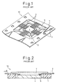
- FIG. 1 is a perspective view of a semiconductor device of the related art obtained by connecting a semiconductor chip and TCP leads. It shows the state before the individual TCPs are cut from the tape.
- the TCP 10 uses a resin film (for example, a polyimide resin film) 1 as a substrate and has leads 2 formed by etching of a copper foil on top. Further, sprocket holes 3 are formed at the two side edges of the resin film 1 for feeding the film. An opening 5 for accommodating a semiconductor chip 4 (in general called a "device hole”) and window holes 9 are also formed in the center of the resin film 1 as illustrated.
- a resin film for example, a polyimide resin film
- leads 2 formed by etching of a copper foil on top.
- sprocket holes 3 are formed at the two side edges of the resin film 1 for feeding the film.
- An opening 5 for accommodating a semiconductor chip 4 (in general called a "device hole”) and window holes 9 are also formed in the center of the resin film 1 as illustrated
- Fig. 2 shows the center portion of the semiconductor device of Fig. 1 enlarged.
- a semiconductor chip 4 is positioned and placed in the device hole 5 of the resin film 1, then the front ends of the leads 2 are bonded on the bumps on the electrodes (normally projections formed by gold plating).
- the leads are normally bonded all together using a special bonding tool.
- the bumps are gold plated in advance before the bonding step.
- the semiconductor chip 4 and the leads 6 are protected from the humidity, contamination, etc. of the ambient environment by sealing the two to cover them by a resin 7.
- the sealing resin 7 use is made for example of an epoxy resin.
- An object of the present invention is to solve the above problems in the related art and provide a semiconductor device, in particular a thin semiconductor package, which reduces and simultaneously achieves a uniform mounting height, does not require complicated steps for mounting individual chips, improves the manufacturing yield, achieves a uniform height of the semiconductor device without being affected by the variation in thickness of the chips, and enables execution of electrical tests all together and a process for production of the same.
- a semiconductor device provided with an insulating tape substrate having through holes in the thickness direction; a semiconductor element mounted on a top surface of the tape substrate with its back surface exposed upward and its active surface facing downward; a sealing resin layer formed on the top surface of the tape substrate outside of the region in which the semiconductor device is mounted and sealing the area around the side surfaces of the semiconductor element; metal interconnections formed on the bottom surface of the tape substrate and blocking the bottom ends of the through holes of the tape substrate to define bottom portions; a solder resist layer covering the metal interconnections and the bottom surface of the tape substrate and having through holes in the thickness direction; external connection terminals projecting from the bottom surface of the metal interconnections and filling, passing through, and projecting downward through the through holes of the solder resist layer; connection terminals extending downward from the active surface of the semiconductor element and inserted in the through holes of the tape substrate; and a filler comprised of a conductive material filling the gaps between the connection terminals and the inside walls
- a process of production of a semiconductor device of the first aspect comprising forming through holes in the thickness direction in a tape substrate having an area able to accommodate a plurality of semiconductor package units and provided at its bottom surface with a metal interconnection layer and a solder resist layer and in the solder resist layer; filling a conductive material in the through holes of the tape substrate in amounts incompletely filling the through holes; inserting connection terminals of a number of semiconductor elements required for forming a plurality of semiconductor package units into the corresponding through holes of the tape substrate and filling the gaps between the connection terminals and the inside walls of the through holes by the conductive material until about the top ends of the through holes; bonding and mounting semiconductor elements on the top surface of the tape substrate; forming a sealing resin layer covering the top surface of the tape substrate other than the regions where the semiconductor elements are mounted and sealing the area around the side surfaces of the semiconductor element; grinding and polishing to a predetermined thickness the top part of the sealing resin layer and the back surface portions of the semiconductor elements
- connection terminals extending downward from the active surface of the semiconductor element and inserted into the through holes of the tape substrate and a filler comprised of a conductive material filling the gap between the connection terminals and the inner walls of the through holes of the tape substrate and electrically connecting the connection terminals and metal interconnections
- a filler comprised of a conductive material filling the gap between the connection terminals and the inner walls of the through holes of the tape substrate and electrically connecting the connection terminals and metal interconnections
- the back surfaces of the semiconductor elements and the sealing resin layer can be ground and polished from the top to reduce the height to a predetermined value in a state with a large number of semiconductor elements fixed to the tape substrate and with the area around the side surfaces of the semiconductor elements sealed by a resin, the individual semiconductor chips can be handled in a thick state without being made thin, no complicated steps or special carriers are required as in the past, a large number of semiconductor package units can be produced all together while integrally fixed to the tape substrate, the heights of the semiconductor devices, that is, the semiconductor packages, can be made small and uniform, the electrical tests can be performed all at once, the production process is shortened and the manufacturing yield improved, and the devices can be made thinner than in the past.
- the semiconductor device is further provided with conductor columns passing through the resin sealing layer and the tape substrate at a region where the resin sealing layer is formed, having top ends exposed at the top surface of the resin sealing layer, and having bottom ends electrically connected to the metal interconnection layer or is further provided with, instead of the sealing resin layer, an insulating frame bonded to the top surface of the tape substrate other than at the region where the semiconductor element is mounted and surrounding the side surfaces of the semiconductor element with a gap and a resin sealing layer filling the gap and sealing the area around the side surfaces of the semiconductor element and further provided with conductor columns passing through the frame and the tape substrate at a region where the frame is formed, having top ends exposed at the top surface of the frame, and having bottom ends electrically connected to the metal interconnection layer.
- a multilayer semiconductor device produced in this way is comprised of a plurality of such semiconductor devices stacked in layers, wherein the semiconductor devices of each layer are connected with each other at the top ends of the conductor columns and the bottom ends of the external connection terminals.
- connection terminals extending downward from the active surface of the semiconductor element are bumps comprised of gold or copper.
- the external connection terminals filling and passing through the openings of the solder resist layer are arranged a peripheral or area array mode according to the application of the semiconductor device or the requirements of the customer.
- the filler is filled in the gaps between the connection terminals and the through holes of the tape substrate up to positions of substantially the top ends of the through holes. That is, the amount of the filler is set so that the total volume with the connection terminals of the semiconductor element inserted later becomes substantially equal to the volume of the through holes of the tape substrate (with bottom portions defined by the metal interconnections). Due to this, the connection terminals and metal interconnections are reliably connected and, simultaneously, overflow of excess conductive material from the top ends of the through holes is prevented.
- the conductive material use may be made of a low melting point metal or a conductive paste.
- the heights of the large number of semiconductor package units formed on the tape substrate are made uniform, it is possible to easily perform electrical tests all together after forming the sealing resin layer and before or after the grinding and the polishing.
- the tape substrate is of a size able to accommodate the plurality of semiconductor package units and is shaped as a disk of 2 to 12 inches in diameter. Due to this, it is possible to use existing grinding machines or cutting machines or other facilities for processing semiconductor wafers of the same size, so the cost of new equipment can be reduced by that amount.
- the top surface of the sealing resin layer and the back surface of the semiconductor element form substantially the same plane.
- the semiconductor device of the second aspect of the present invention may be produced by one of the following three processes of production depending on whether it is provided with the conductor columns, the external connection terminals, or both.
- a process of production of a semiconductor device comprising preparing a tape substrate having an area able to accommodate a plurality of semiconductor package units, provided at its top surface with metal interconnections, having through holes in a thickness direction at positions corresponding to external connection terminals, and having bottom surfaces of the metal interconnections defining top ends of the through holes; bonding connection terminals of active surfaces of a number of semiconductor elements required for forming the plurality of semiconductor package units to the top surfaces of the metal interconnections of the tape substrate to mount the semiconductor elements on the top surface of the tape substrate; forming a sealing resin layer sealing the area around the side surfaces of the semiconductor elements, including the metal interconnections, and filling the gaps between the active surfaces of the semiconductor elements and the top surface of the tape substrate; then, in either order, grinding and polishing to a predetermined thickness the top part of the sealing resin layer and the back surface portions of the semiconductor elements and forming external connection terminals extending downward from the bottom surfaces of the metal interconnections defining the top ends of the through holes, filling the
- a process of production of a semiconductor device comprising preparing a tape substrate having an area able to accommodate a plurality of semiconductor package units, provided at its top surface with metal interconnections, having through holes in a thickness direction at positions corresponding to external connection terminals, and having bottom surfaces of the metal interconnections defining top ends of the through holes; bonding connection terminals of active surfaces of a number of semiconductor elements required for forming the plurality of semiconductor package units to the top surfaces of the metal interconnections of the tape substrate to mount the semiconductor elements on the top surface of the tape substrate; forming conductor columns with bottom ends bonded to the top surfaces of the metal interconnections; forming a sealing resin layer sealing the area around the side surfaces of the semiconductor elements, including the metal interconnections and conductor columns, and filling the gaps between the active surfaces of the semiconductor elements and the top surface of the tape substrate; then, in either order, grinding and polishing to a predetermined thickness the top part of the sealing resin layer and the back surface portions of the semiconductor elements and exposing the top ends of the
- connection terminals projecting downward from the active surface of the semiconductor element be connected to the top surfaces of the metal interconnections on the top surface of the tape substrate, it is possible to further simplify the structure than when connecting the connection terminals and the metal interconnections through a filler in the through holes of the tape substrate as in the first aspect of the invention and therefore it is possible to further improve the productivity of thin semiconductor devices.
- a semiconductor device provided with a resin member of a predetermined thickness; a semiconductor element sealed inside the resin member, having a back surface exposed at a top surface of the resin member, and having an active surface facing downward; metal interconnections formed on the bottom surface of the resin member; and connection terminals extending downward from the active surface of the semiconductor element and having a bottom end connected to top surfaces of the metal interconnections.
- the top surface of the sealing resin layer and the back surface of the semiconductor element form substantially the same plane.
- a process of production of a semiconductor device of the third aspect comprising mounting on the top surface of a metal substrate having an area able to accommodate a plurality of semiconductor package units semiconductor elements by turning the active surfaces of semiconductor elements downward and bonding front ends of connection terminals to the metal substrate; covering the entire top surface of the metal substrate by a resin to form a resin member in which the semiconductor elements are sealed and to the bottom surface of which the metal substrate is bonded; then, in either order, grinding and polishing to a predetermined thickness the top part of the sealing resin layer and the back surface portions of the semiconductor elements and patterning the metal substrate to form metal interconnections with top surfaces connected to the bottom ends of the connection terminals on the bottom surface of the resin member; and cutting the resin member into semiconductor package units to obtain individual semiconductor devices.
- a process of production of a semiconductor device of the third aspect comprising preparing a composite metal plate comprised of a metal substrate having an area able to accommodate a plurality of semiconductor package units and of an interconnection pattern comprised of a different type of metal from the metal substrate on its top surface; mounting semiconductor elements on the top surface of the composite metal plate by turning the active surfaces of semiconductor elements downward and bonding front ends of connection terminals to the composite metal plate; covering the entire top surface of the composite metal plate by a resin to form a resin member in which the semiconductor elements are sealed and to the bottom surface of which the composite metal plate is bonded; then, in either order, grinding and polishing to a predetermined thickness the top part of the resin member and the back surface portions of the semiconductor elements and etching away the metal substrate of the composite metal plate and leaving the interconnection pattern so as to form metal interconnections comprised of the interconnection pattern with top surfaces connected to the bottom ends of the connection terminals on the bottom surface of the resin member; and cutting the resin member into semiconductor package units to
- the individual semiconductor chips can be handled in a thick state without being made thin, no complicated steps or special carriers are required as in the past, a large number of semiconductor package units can be produced all together while integrally fixed in the resin member, the heights of the semiconductor devices, that is, the semiconductor packages, can be made small and uniform, the electrical tests can be performed all at once, the production process is shortened and the manufacturing yield improved, and the devices can be made thinner than in the past.
- the side surfaces of the conductor columns are exposed at the side surfaces of the resin member. Due to this, it is also possible to easily obtain a parallel semiconductor device comprised of a plurality of semiconductor devices connected to each other at their side surfaces, wherein the semiconductor devices adjoining each other at their sides are electrically connected with each other at the side surfaces of the conductor columns exposed at the side surfaces of the resin member.
- a multilayer parallel semiconductor device comprised of a plurality of semiconductor devices stacked in layers and connected to each other at their side surfaces, wherein the semiconductor devices of each layer are electrically connected with each other at the top ends of the conductor columns and the bottom ends of the metal interconnections through connection bumps and wherein the semiconductor devices adjoining each other at their sides are electrically connected with each other at the side surfaces of the conductor columns exposed at the side surfaces of the resin member.
- the semiconductor device is further provided with a solder resist layer covering the entire bottom surface of the resin member including the metal interconnections and connection bumps formed on the bottom surfaces of the metal interconnections, passing through the solder resist layer, and projecting downward.
- the semiconductor device is further provided with a capacitor sealed inside the resin member and directly connected with the metal interconnections.
- the capacitor is a multilayer ceramic capacitor including inner electrodes each having the surface being perpendicular to the thickness direction of the resin member.
- an inorganic filler is dispersed in the resin member. Due to this, it is possible to adjust the thermal expansion coefficient and the heat conductivity of the resin member to desired values.
- Figure 3 shows, (1) sectional and (2) top views, an example of a semiconductor device according to the first aspect of the present invention.
- the illustrated semiconductor device 20 is comprised of an insulating tape substrate 21 having through holes 22 in the thickness direction and a semiconductor element 23 bonded to its top surface with a back surface 23B exposed upward and with an active surface 23A facing downward.
- a sealing resin layer 24 is formed on a region 21Y of the top surface of the tape substrate other than the region 21X where the semiconductor element 23 is bonded and seals the area around the side surfaces of the semiconductor element 23.
- the metal interconnections 25 formed on the bottom surface of the tape substrate 21 block the bottom ends of the through holes 22 of the tape substrate 21 and define bottom portions.
- a solder resist layer 26 having through holes 27 in the thickness direction covers the bottom surfaces of the metal interconnections 25 and the tape substrate 21.
- connection terminals 28 projecting from the bottom surface of the metal interconnections 25 fill and pass through the through holes 27 of the solder resist layer 23A and project downward.
- Connection terminals 29 extending downward from the active surface 23A of the semiconductor element 23 are inserted into the through holes of the tape substrate 21.
- the connection terminals 29 and the metal interconnections 25 are electrically connected by the filler 30 of the low melting point metal filled in the gaps between the connection terminals 29 and the inside walls of the through holes 22 of the tape substrate 21.
- a conductive paste may be used instead of the low melting point metal.
- the conductive paste generally use is made of a silver paste or copper paste comprised of a polyimide resin or epoxy resin in which silver or copper particles are dispersed. These conductive pastes are filled in the through holes by screen printing etc.
- the back surface of the semiconductor element 23 and the top surface of the sealing resin layer 24 are on the same plane, but so long as the sealing resin layer 24 seals the area around the side surfaces of the semiconductor element 23, they do not necessarily have to be in the same plane.
- the height of the sealing resin layer 24 may also be made lower than the back surface of the semiconductor element 23 at a location away from the side surfaces of the semiconductor element 23.
- FIG 4 shows the initial structure which is initially prepared.
- the tape substrate 21 has an area able to accommodate a plurality of semiconductor package units and is provided at its bottom surface with a metal interconnection layer 25 and solder resist layer 26.
- various organic materials or polymer materials may be used. In general, however, a polyimide film, a glass or aramide or other fiber reinforced epoxy film or bismaleimide triazine (BT) film, polyphenylene ether (PPE) film, or other resin film or resin sheet is suitable.
- the thickness of the tape substrate 21 is preferably as thin as possible for reducing the thickness of the semiconductor device to the extent where the strength and rigidity necessary for the substrate are secured. In general, it is in the range of 25 ⁇ m to 100 ⁇ m, in particular around 75 ⁇ m.
- Through holes 22 are formed in the tape substrate 21 by punching etc., then a copper foil is adhered on one surface to form a metal interconnection layer 25.
- a copper foil clad tape combining a tape substrate 21 and copper foil is used and the tape substrate 21 portion laser processed to form holes passing through the tape substrate 21 and having the copper foil as bottom portions.
- the copper foil clad tape is obtained by forming an insulating layer on a copper foil by coating polyimide or another resin.
- a filler 30 of a low melting point metal is incompletely filled in the through holes 22 of the tape substrate 21 (with bottom portions defined by the metal interconnection layer 25). That is, the amount of filler is made so that the filler 30 fills the gaps between the connection terminals 29 and the inside walls of the through holes 22 up to substantially the top ends of the through holes 22 when the connection terminals 29 of the semiconductor elements 21 are inserted in a later step.
- the low melting point metal of the filler 30 use may be made of a silver-tin alloy (Ag-Sn), a lead-tin alloy (Pb-Sn), a silver-tin-copper alloy (Ag-Sn-Cu), and alloys of these with bismuth (Bi) or antimony (Sb).
- the filler is preferably filled by electrolytic plating using the copper foil as the layer supplying the power, but it may also be filled by screen printing a solder paste.
- solder resist layer 26 having through holes 27 is formed.
- the solder resist layer 26 having through holes 27 is formed by generally formed by coating, exposing, and developing a photosensitive resist.
- the layer may also be formed by screen printing a resin.
- the through holes 27 of the solder resist layer 26 are formed in a peripheral or area array in accordance with the application of the semiconductor devices 20 to be produced.
- an insulating coating 31 comprised of a liquid or a semicured resin is coated on the top surface of the tape substrate 21.
- the semicured insulating coating 31 acts to bond the semiconductor elements.
- the semiconductor elements 23 are arranged on and bonded to the precured coating 31. That is, the connection terminals 29 of the number of semiconductor elements 23 necessary for forming the plurality of semiconductor package units are inserted into the corresponding through holes 22 of the tape substrate 21, the gaps between the connection terminals 29 and the inside walls of the through holes 22 are filled with the low melting point metal 30 up to substantially the top ends of the through holes 22, and the semiconductor elements 23 are bonded to and mounted on the top surface of the tape substrate 21. This is done by heating the semiconductor elements 23 to a temperature near the melting point of the low melting point metal 30 and pushing the connection terminals 29 into the low melting point metal 30 in the through holes 22.
- connection terminals 29 of the semiconductor elements 23 are desirably formed as gold or copper bumps.
- the connection terminals 29 are formed as stud bumps using the wire bonding method.
- the connection terminals 29 are desirably formed by plating from the viewpoint of avoiding mechanical shock resulting from the formation of stud bumps.
- the plating method is particularly advantageous when forming bumps in an area array along with the interconnection portion on the semiconductor elements.
- Stud bumps are desirably formed by gold.
- Plated bumps are desirably formed as copper posts provided with protective plating layers.
- the size of the connection terminals may be freely set in accordance with the design thickness of the semiconductor devices 20.
- the bumps 29 have a diameter of the bottom portions of 70 ⁇ m and a height of 30 to 60 ⁇ m.
- the through holes 22 of the tape substrate 21 in which the bumps 29 are inserted suitably have diameters in the range of 90 to 150 ⁇ m.
- a sealing resin layer 24 covering the top surface of the tape substrate 21 at other than the regions where the semiconductor elements 23 are mounted and sealing at least the areas around the side surfaces of the semiconductor elements 23 is formed. Note that in Fig. 7 to Fig. 9, an extremely thin insulating coating 31 is illustrated together with the sealing resin layer 24 and is not illustrated separately.
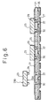
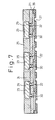
- Figure 7 shows the state where the sealing resin layer 24 covers also the semiconductor elements 23 and is formed to a substantially identical thickness overall.
- the sealing resin layer 24 does not necessarily have to cover the semiconductor elements 23 at the stage of this step.
- the thickness of the sealing resin layer 24 may also be made the same as the height of the semiconductor elements 23 at the contact portions with the side surfaces of the semiconductor elements 23 and made thinner at the regions away from the semiconductor elements 23. That is, the thickness of the sealing resin layer 24 formed at the stage of this step may be set so that a thickness enabling the areas around the side surfaces of the semiconductor elements 23 to be completely sealed is left after the grinding and polishing performed in the next step.
- the top part of the sealing resin layer 24 and the back surface 23B portions of the semiconductor elements 23 are ground and polished to a predetermined thickness. Due to this, for example, it is possible to make semiconductor elements 23 of a thickness of around 500 ⁇ m in the state of Fig. 7 or Fig. 8 a thin 50 to 100 ⁇ m. As a result, the semiconductor devices 20 can be reduced to a thickness of 120 to 300 ⁇ m. This is less than 1/4 of the approximately 1200 ⁇ m thickness of the thin-small outline package (TSOP) most frequently used in the past.
- TSOP thin-small outline package
- solder resist layer 26 After the grinding and polishing, external connection terminals 28 projecting from the bottom surface of the solder resist layer 26 are formed in the through holes 27 of the solder resist layer 26. This can be done by reflowing after placing solder balls or screen printing solder paste.
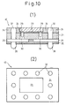
- the illustrated semiconductor device 40 includes, in addition to the structure shown in Fig. 3, low melting point metal conductors (conductor columns) 32.
- the conductors 32 pass through the sealing resin layer 24 sealing the area around the side surfaces of the semiconductor element 23 and the tape substrate 21 at regions where the sealing resin layer 24 is formed, have top ends exposed at the top surface of the sealing resin layer 24, and have bottom ends electrically connected to the metal interconnection layer 25.
- a plurality of the semiconductor devices 40 of Fig. 10 may be stacked in layers as shown in Fig. 11 to form a thin multilayer semiconductor device 44. That is, by connecting the top ends of the low melting point metal conductors 32 of a bottom semiconductor device 40 and the bottom ends of the external connection terminals 28 of a top semiconductor device 40, a single semiconductor device 4 comprised of an integral circuit including a plurality of semiconductor elements 23 (in this example, three) in a multilayer structure is formed.
- the semiconductor devices 40 may be stacked as follows:
- a plurality of semiconductor devices are positioned and stacked by a fixture having the external shape of the semiconductor devices (external guide), then the metal is made to reflow all together in the state with a suitable load applied in the stacking direction, whereby a multilayer semiconductor device is formed.
- a plurality of semiconductor devices are stacked while positioning them by passing pins through guide holes provided in the individual semiconductor devices, then the metal is made to reflow all together in the state with a suitable load applied in the stacking direction.
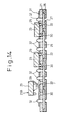
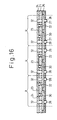
- FIG. 10 An example of the process of production of a semiconductor device of the first aspect of the present invention shown in Fig. 10 will be explained next with reference to Figs. 12 to 16. Portions corresponding to the structure of the first embodiment shown in Fig. 4 to Fig. 9 are assigned the same reference numerals as in Fig. 4 to Fig. 9.
- the initial structure shown in Fig. 12 is the same as the initial structure of the first embodiment shown in Fig. 4 except that through holes 33 are formed in the tape substrate 21 in addition to the through holes 22.
- the through holes 22 are provided at positions corresponding to the connection terminals 29 of the semiconductor elements 23 in the same way as in the first embodiment, while the through holes 33 are provided in the regions of formation of the sealing resin layer 24 sealing the areas around the side surfaces of the semiconductor elements 23.
- the through holes 33 are several times larger in diameter than the through holes 22. For example, when the through holes 22 have a diameter of about 25 to 100 ⁇ m, the through holes 33 have a diameter of about 500 ⁇ m.
- a small amount of flux 34 is placed in each through hole 33 with a bottom surface defined by the metal interconnection layer 25.
- the rest of the initial structure shown in Fig. 12 is formed by processing similar to the first embodiment.
- low melting point metal conductors 32 projecting from the top surface of the sealing resin layer 24 are formed in the through holes 33. This is done by placing balls of the low melting point metal, for example, solder balls, on the flux 34 in the through holes 33 and reflowing them. Next, the same procedure is followed as in the first embodiment to form the insulating coating 31.
- connection terminals 29 projecting upward from the active surfaces 23A of the semiconductor elements 23 are inserted into the through holes 22 of the tape substrate 21 and pushed into the low melting point metal 30.
- a sealing resin layer 24 covering the top surface of the tape substrate 21 at other than the regions where the semiconductor elements 23 are mounted and sealing at least the areas around the side surfaces of the semiconductor elements is formed.
- the illustration of the insulating coating 31 is omitted.
- Figure 15 shows the state where the sealing resin layer 24 covers also the semiconductor elements 23 and is formed to a substantially identical thickness overall. As shown in Fig. 8 relating to the first embodiment, however, the sealing resin layer 24 does not necessarily have to cover the semiconductor elements 23 at the stage of this step.
- the thickness of the sealing resin layer 24 may also be made the same as the height of the semiconductor elements 23 at the contact portions with the side surfaces of the semiconductor elements 23 and made thinner at the regions away from the semiconductor elements 23. That is, the thickness of the sealing resin layer 24 formed at the stage of this step may be set so that a thickness enabling the areas around the side surfaces of the semiconductor elements 23 to be completely sealed is left after the grinding and polishing performed in the next step.
- the top part of the sealing resin layer 24, the top parts of the conductors 32, and the back surface 23B portions of the semiconductor elements 23 are ground and polished to a predetermined thickness.
- external connection terminals 28 are formed in the through holes 27 of the solder resist layer 26 in the same way as in the first embodiment.
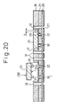
- Figure 17 shows still another example of the semiconductor device according to the first aspect of the present invention, in (1) sectional and (2) top views. Portions corresponding to the structure of the first embodiment shown in Fig. 3 are assigned the same reference numerals as in Fig. 3.
- the illustrated semiconductor device 60 includes, instead of the sealing resin layer 24 in the structure shown in Fig. 3, an insulating frame 36 bonded to the top surface of the tape substrate 21 other than at the region where the semiconductor element 23 is mounted and surrounding the side surfaces of the semiconductor element 23 with a gap G and a resin sealing layer 24 filling the gap G and sealing the area around the side surfaces of the semiconductor element 23 and further includes column-shaped conductors (conductor columns) of a low melting point metal passing through the frame 36 and the tape substrate 21 at a region where the frame 36 is formed, having top ends exposed at the top surface of the frame 36, and having bottom ends electrically connected to the metal interconnection layer 25.
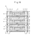
- a plurality of the semiconductor devices 60 of Fig. 17 may be stacked in layers as shown in Fig. 18 to form a thin multilayer semiconductor device 66. That is, by connecting the top ends of the low melting point metal column-shaped conductors 32 of a bottom semiconductor device 60 and the bottom ends of the external connection terminals 28 of a top semiconductor device 60, a single semiconductor device 66 comprised of an integral circuit including a plurality of semiconductor elements 23 (in this example, three) in a multilayer structure is formed.
- the semiconductor devices 60 may be stacked in the same way as shown in the second embodiment.
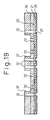
- the initial structure shown in Fig. 19, in addition to the structure shown in Fig. 4, has an insulating substrate 36 having openings 37 at regions for mounting the semiconductor elements 23 bonded to the top surface of the tape substrate 21 and is formed with column-shaped conductors 32 passing through the tape substrate 21 and the insulating substrate 36.
- the openings 37 as shown in Fig. 17(2), have shapes and dimensions enabling semiconductor elements 23 to be accommodated with a gap G.
- the through holes 22 of the tape substrate 21 are provided at positions corresponding to the connection terminals 29 of the semiconductor elements in the same way as in the first embodiment.
- the insulating substrate 36 is a tape of the same outer shape as the tape substrate 21 and is bonded to the top surface of the tape substrate 21 after forming the openings 37 by punching etc.
- through holes passing through the insulating substrate 36 and tape substrate 21 are formed by laser processing at positions forming the column-shaped conductors 32.
- the column-shaped conductors 32 are formed by plating to bury the holes using the copper foil before patterning to the metal interconnection layer 25 as the layer to supply the power.
- the rest of the portions of the initial structure of Fig. 19 are formed by processing similar to the first embodiment.
- the column-shaped conductors 32 are several times larger in diameter than the through holes 22. For example, when the through holes 22 have a diameter of about 25 to 100 ⁇ m, the column-shaped conductors 32 have a diameter of about 500 ⁇ m.
- an insulating coating 31 is formed on the top surface of the tape substrate 21 exposed inside the openings 37, then the same procedure is followed as in the first embodiment to arrange and bond the semiconductor elements 23 on the precured coating 31.
- the connection terminals 29 projecting up from the active surfaces 23A of the semiconductor elements 23 are inserted into the through holes 22 of the tape substrate 21 and pushed into the low melting point metal 30.
- the gaps G between the semiconductor elements 23 and the openings 37 of the insulating substrate 36 are sealed by the sealing resin layer 24. Due to this, the areas around the side surfaces of the semiconductor elements 23 are sealed.
- the illustration of the insulating coating 31 is omitted.
- the top part of the insulating substrate 36, the top part of the sealing resin layer 24, the top parts of the conductors 32, and the back surface 23B portions of the semiconductor elements 23 are ground and polished to a predetermined thickness.
- external connection terminals 28 are formed in the through holes 27 of the solder resist layer 26 in the same way as in the first embodiment.
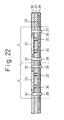
- Figure 23 shows, as the initial structure including the tape substrate 21, a disk shaped structure of a diameter of 2 inches to 12 inches before cutting.
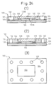
- Figure 24 shows, in (1) sectional, (2) sectional and (3) top views, an example of a semiconductor device according to the second aspect of the present invention. Portions corresponding to the structures of the first to fourth embodiments are assigned reference numerals off those embodiments plus 100 (same in the following embodiments as well).
- the illustrated semiconductor device 101 is comprised of an insulating substrate 121, metal interconnections 125 formed on its top surface, and a semiconductor element 123 mounted with its back surface 123B exposed upward and with its active surface 123A facing downward.
- the bottom ends of the connection terminals 129 projecting downward from the active surface 1223A of the semiconductor element 123 are connected to the top surfaces of the metal interconnections 125.
- a sealing resin layer 124 formed on the top surface of the tape substrate 121 seals the area around the side surfaces of the semiconductor element 123 and fills the gap between the active surface 123A of the semiconductor element 123 and the bottom surface of the tape substrate 121.
- the conductor columns 132 extend upward from the top surfaces of the metal interconnections 125, pass through the sealing resin layer 124 at the areas around the side surfaces of the semiconductor element 123, and have top ends exposed upward.
- the conductor columns 132 may be substantially ball shaped as shown in Fig. 24A (more accurately, entasis shaped) or may be rod shaped as shown in Fig. 24B.
- the conductor columns 132 are columns or balls of a metal such as copper or nickel etc. Preferably they are balls of a low melting point metal such as solder.
- solder use may be made of silver-tin alloy (Ag-Sn), a lead-tin alloy (Pb-Sn), a silver-tin-copper alloy (Ag-Sn-Cu), and alloys of these with bismuth (Bi) or antimony (Sb).
- FIG. 25 a process of production of the semiconductor device 101 shown in Fig. 24 will be explained.
- This embodiment can be used when producing a large number of semiconductor package units all together in the same way as the first to fourth embodiments. Below, however, for simplification of the explanation, the explanation will be given of the production of a single semiconductor package unit.
- connection terminals 129 on its active surface 123A and a tape substrate 121 provided with metal interconnections 125 on its top surface are prepared.
- the method of formation of the connection terminals 129, the materials and configuration of the tape substrate 121, and the method of formation of the metal interconnections 125 are similar to those of the first embodiment.
- connection terminals 129 of the active surface 123A of the semiconductor element 123 are bonded to the top surfaces of the metal interconnections 125 of the tape substrate 121 so as to place the semiconductor element 123 on the top surface of the tape substrate 121.
- This bonding (mounting) may be performed in the following way.
- connection terminals 129 are heated and press bonded to metal (solder) layers formed at predetermined positions of the metal interconnections 125 by plating etc. in advance or connection terminals 129 comprised of gold bumps are placed on the gold plating on the metal interconnections 125 and directly bonded or bonded through an anisotropic conductive film or paste by application of ultrasonic waves.
- conductor columns 132 with bottom ends bonded to the top surfaces of the metal interconnections 125 are formed.
- the conductor columns 132 are substantially ball shaped as shown in Fig. 24(2) (more accurately entasis shaped) and consist of solder balls.
- Conductor columns 132 using solder balls may be formed by placing solder balls at predetermined locations on the top surface of the metal interconnections 125 or screen printing solder paste, then reflowing the metal.
- the conductor columns 132 may also be rod shaped as shown in Fig. 24(2).
- the rod shaped conductor columns 132 may be formed in the following way.
- Rod shaped members of metal preferably copper, plated on their surfaces with solder, tin (Sn), indium (In), etc. are bonded by heating and pressure at predetermined locations of the top surfaces of the metal interconnections 125 or predetermined locations of the top surfaces of the metal interconnections 125 are plated by solder etc., then rod-shaped members are mounted and the solder made to reflow.
- the sealing resin layer 124 seals the area around the side surfaces of the semiconductor element 123 including the metal interconnections 125 and the conductor columns 132 and fills the gap between the active surface 123A of the semiconductor element 123 and the top surface of the tape substrate 121.
- the sealing resin layer 124 may be formed by molding or dotting.
- the top part of the sealing resin layer 24 and the back surface portion of the semiconductor element 123 are ground and polished to a predetermined thickness.
- the top surface of the sealing resin layer 124 is in the same plane as the top surface (back surface) of the semiconductor element 123, but this is not necessarily required. It is sufficient to set the thickness of the sealing resin layer 124 so that the top ends of the conductor columns 132 are exposed upward when the entire assembly, including the semiconductor element 123, is reduced to the predetermined thickness by the grinding and polishing of Fig. 25(5).
- Figure 25 shows only one semiconductor package unit, but it is also possible to produce a large number of semiconductor package units all together by the steps (1) to (5) of Fig. 25 using a tape substrate 121 of an area able to accommodate a plurality of semiconductor package units. In this case, it is possible to finally cut the tape substrate 121 into semiconductor package units to obtain individual semiconductor devices 101 (Fig. 24).
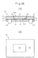
- Figure 26 shows, in (1) sectional and (2) top views, another example of a semiconductor device according to the second aspect of the present invention.
- the external connection terminals 128 extend downward from the bottom surfaces of the metal interconnections 125, pass through the tape substrate 121, and project downward.
- the rest of the structure is the same as in the fifth embodiment.
- the material of the external connection terminals 128 can be selected from the same materials as used for the conductor columns 132.
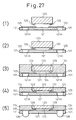
- FIG. 27 a process of production of the semiconductor device 102 shown in Fig. 26 will be explained next.
- the present embodiment may be applied to the case of producing a large number of semiconductor package units all together in the same way as in the first to fourth embodiments, but for simplification of the explanation, the explanation will be given below of production of a single semiconductor package unit.
- a semiconductor element 123 provided with connection terminals 129 on its active surface 123A and a tape substrate 121 are prepared.
- the tape substrate 121 is provided with metal interconnections 125 on its top surface, has through holes 121H in the thickness direction at positions corresponding to the external connection terminals 128, and has bottom surfaces of the metal interconnections 125 blocking the top ends of the through holes 121H and demarcating them.
- the method of formation of the connection terminals 129, the materials and configuration of the tape substrate 121, and the method of formation of the metal interconnections 125 are similar to those of the first embodiment.
- the method of formation of the through holes 121H is similar to that of the through holes 22 of the first embodiment.
- a semiconductor element is mounted on the top surface of the tape substrate 121 in the same way as the step of Fig. 25(2) of the fifth embodiment.
- a sealing resin layer 124 is formed in the same way as the step of Fig. 25(4) of the fifth embodiment.
- the top part of the sealing resin layer 124 and the back surface portion of the semiconductor element 123 are ground and polished to a predetermined thickness.
- the top surface of the sealing resin layer 124 is higher than the top surface (back surface) of the semiconductor element 123 and the entire semiconductor element 123 is embedded inside the sealing resin layer 124, but this is not necessarily required. It is sufficient to set the thickness of the sealing resin layer 124 so as to enable the entire assembly, including the semiconductor element 123, to be made a predetermined thickness by the later grinding and polishing.
- the external connection terminals 128 are formed.
- the external connection terminals 128 extend downward from the bottom surfaces of the metal interconnections 125 defining the top ends of the through holes 121H, fill the through holes 121H, and project downward.
- the step of grinding and polishing of Fig. 27(4) and the step of forming the external connection terminals of Fig. 27(5) may be performed in that order or in a reverse order.
- Figure 27 shows only one semiconductor package unit, but it is also possible to produce a large number of semiconductor package units all together by the steps (1) to (5) of Fig. 27 using a tape substrate 121 of an area able to accommodate a plurality of semiconductor package units. In this case, it is possible to finally cut the tape substrate 121 into semiconductor package units to obtain individual semiconductor devices 102 (Fig. 26).
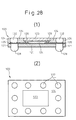
- Figure 28 shows, in (1) sectional and (2) top views, another example of the semiconductor device according to the second aspect of the invention.
- both the conductor columns 132 of the fifth embodiment and the external connection terminals 128 of the sixth embodiment are provided.
- the process of production of the semiconductor device 103 of the present embodiment is a combination of the process of production of the fifth embodiment and the process of production of the sixth embodiment.
- the semiconductor device 103 shown in Fig. 28 may also be stacked in a plurality of layers.
- a semiconductor element 123 shown in Fig. 27(1) and a tape substrate 121 are prepared.
- the semiconductor element is mounted on the top surface of the tape substrate 121 as shown in Fig. 27(2).
- conductor columns 132 with bottom ends bonded to the top surfaces of the metal interconnections 125 are formed.
- a sealing resin layer 124 is then formed.
- the semiconductor devices according to the first and second aspects of the present invention explained above include tape substrates. Below, an explanation will be given of embodiments of a semiconductor device according to a seventh aspect of the present invention not including a tape substrate.
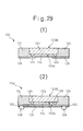
- FIG. 29 shows, in sectional views, an example of a semiconductor device according to the seventh aspect of the present invention.
- the semiconductor device 104 shown in Fig. 29(1) is comprised of a resin member 124 of a predetermined thickness in which a semiconductor element 123 is sealed.
- the semiconductor element 123 has a back surface 123B exposed at the top surface of the resin member 124 and has an active surface 123A facing downward.
- Metal interconnections 125 are formed at the bottom surface of the resin member 124.
- Connection terminals 129 extending downward from the active surface 123A of the semiconductor element 123 are connected to the top surfaces of the metal interconnections 125.
- the top surface of the resin member 129 and the back surface 123B of the semiconductor element 123 form the same plane.
- the connection terminals 129 are formed as gold stud bumps, plated bumps, etc.
- the semiconductor device 104' shown in Fig. 29(2) is structured the same as the semiconductor device 104 of Fig. 29(1) except that the bottom surface of the resin member, including the metal interconnections 125, is covered by a solder resist layer 126 and that connection bumps 128 formed on the bottom surfaces of the metal interconnections 125 pass through the solder resist layer 126 and project downward.
- FIG. 30 an explanation will be given of the process of production of the semiconductor devices 104 and 104' shown in Fig. 29.
- the present embodiment can be applied to the case of producing a large number of semiconductor package units all together in the same way as in the first to fourth embodiments, but for simplification of the explanation, an explanation will be made of a single semiconductor package unit.
- the semiconductor element 123 is mounted on a metal substrate 125M by bonding the front ends of the connection terminals 129 formed on the active surface 123A of the semiconductor element 123 on the top surface of a metal substrate 125 such as an aluminum foil, copper foil, copper foil formed with interconnections by metal plating, and aluminum foil clad with copper by a method such as ultrasonic bonding, alloy bonding through a low melting point metal such as indium, etc.
- a metal substrate 125 such as an aluminum foil, copper foil, copper foil formed with interconnections by metal plating, and aluminum foil clad with copper by a method such as ultrasonic bonding, alloy bonding through a low melting point metal such as indium, etc.
- a resin member 124 is formed by covering the entire top surface of the metal substrate 125M with a resin.
- the resin member 124 seals the semiconductor element 123 inside it and has a bottom surface bonded to the metal substrate 125M.
- the resin member 124 use may be made of an epoxy resin, polyimide resin, cyanoester resin, or polycyclic aromatic resin.
- an epoxy resin is desirable.
- silica, alumina, aluminum nitride, and other ceramic particles may be dispersed as an inorganic filler.
- the amount of dispersion is set in accordance with the desired values of the thermal expansion coefficient and heat conductivity.
- the particle size is 2 to 10 ⁇ m.
- the particles are preferably shaped as close to spheres as possible.
- the metal substrate 125M is patterned to form metal interconnections 125 on the bottom surface of the resin member 124.
- the metal interconnections 125 have top surfaces connected to the connection terminals 129.
- top part of the resin member 124 and the back surface portion of the semiconductor element 123 are ground and polished to a predetermined thickness.
- solder resist layer 126 covering the entire bottom surface of the resin member 124 including the metal interconnections 125 is formed, then through holes 127 are formed in the solder resist layer 126.
- the through holes 127 are open at the bottom ends. The top ends are blocked and demarcated by the bottom surfaces of the metal interconnections 125.
- the top part of the resin member 124 and the back surface portion of the semiconductor element 123 are ground and polished to a predetermined thickness.
- external connection terminals 128 filling the through holes 127 and projecting downward are formed. This may be done, in the same way as the conductor columns 132 shown in Fig. 25(3), by placing solder balls or printing solder paste and then reflowing them.
- a composite metal plate comprised of the metal substrate 125M and an interconnection pattern of a different type of metal formed on its top surface is prepared. This is done by providing an aluminum interconnection pattern 125 on a copper substrate 125M comprised of a copper foil by aluminum plating or by providing a copper interconnection pattern 125 on an aluminum substrate 125M by etching and patterning the copper of a copper clad aluminum foil.
- the semiconductor element 123 is mounted on the composite metal plate 125A by bonding the front ends of the connection terminals 129 formed on the active surface 123A of the semiconductor element 123 on the top surface of the interconnection pattern 125 by a method such as ultrasonic bonding or alloy bonding through a low melting point metal such as indium.
- the resin member 124 is formed by covering the entire top surface of the composite metal plate 125A including the interconnection pattern 125 by a resin.
- the resin member 124 seals inside it the semiconductor element 123 and has a bottom surface bonded to the interconnection pattern 125 and the metal substrate 125M.
- the resin member 124 is made of the same material as explained with reference to Fig. 30(2).
- the metal substrate 125M is removed by etching.
- the copper foil substrate 125M is removed by etching using an etchant which dissolves copper, but does not dissolve aluminum.
- the aluminum substrate 125M is removed by etching using an etchant which dissolves aluminum, but does not dissolve copper. Due to this, a structure is obtained where metal interconnections 125 comprised of aluminum or copper are bonded to the bottom surface of the resin member 124.
- the top part of the resin member 124 and the back surface portion of the semiconductor element 123 are ground and polished to a predetermined thickness.
- the above steps complete the semiconductor device 104 shown in Fig. 29(1).
- the position of the bonding surface of the resin member 124 and the solder resist layer 126 is in the same plane as the top surfaces of the metal interconnections 125 in the structure of Fig. 29(1), while is in the same plane as the bottom surfaces of the metal interconnections 125 in the structure obtained in the above steps.
- the formation of the solder resist layer 126, the grinding and polishing, and the formation of the external connection terminals 128 are performed by the same procedure as in steps shown in Figs. 30(4), 30(5), and 30(6).
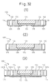
- Figure 32 shows, in sectional views, another example of a semiconductor device according to the seventh aspect of the present invention.
- the semiconductor devices 105, 105', and 105" shown in Figs. 32(1), 32(2), and 32(3) are each further provided with a plurality of conductor columns 132 in addition to the structure of the semiconductor device 104 shown in Fig. 29A.
- the conductor columns 132 pass through the resin member 124 from the top surface of the metal interconnections 125 and extend upward. The top ends are exposed at the top surface of the resin member 124.
- the semiconductor device 105 of Fig. 32(1) only the top ends of the conductor columns 124 are exposed from the resin member 124.
- the top ends and the side surfaces of the conductor columns 132 are exposed from the resin member 124.
- the semiconductor device 105" of Fig. 32(3) is provided with conductor columns 132A with only top ends exposed from the resin member 124 and conductor columns 132B with top ends and side surfaces exposed from the resin member 124.
- the solder resist layer 126 does not cover the portions of the metal interconnections 125 connected with the conductor columns 132B with the side surfaces exposed. The bottom surfaces of the metal interconnections are exposed at these portions.
- the conductor columns 132, 132A, and 132B may be formed by copper (Cu), nickel (Ni), Kovar (tradename), and other metals or alloys or tin-silver (Sn-Ag) alloy, tin-lead (Sn-Pb) alloy, or other low melting point alloys.
- Figure 33 shows an example of a multilayer semiconductor device comprised of a plurality of semiconductor devices 105 shown in Fig. 32(1) stacked in layers.
- the illustrated semiconductor device 106 comprises three semiconductor devices 105 stacked in layers.
- a solder resist layer 126 and connection bumps 128 are formed in the same way as in Fig. 29(2), then the devices are stacked to form an integral unit.
- the top ends of bottom conductor columns 132 and the bottom surfaces of top metal interconnections are electrically connected with each other through the connection bumps 128.
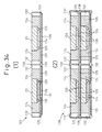
- Figure 34(1) shows an example of a parallel semiconductor device comprised of a plurality of semiconductor devices 105' shown in Fig. 32(2) connected to each other at their side surfaces.
- the illustrated semiconductor device 107 comprises two semiconductor devices 105' connected in parallel.
- the bottom surface of each resin member 124, including the metal interconnections 125, are covered by a solder resist layer 126 except at the side ends.
- the side surfaces of the conductor columns 132 exposed at the side surfaces of the resin members 124 are electrically connected with each other through solder or another low melting point metal 138.
- This connection may be performed as follows. Low melting point metal balls are placed or a low melting point metal paste is printed or a low melting point metal is supplied by dotting, followed by reflowing, whereby the low metal point metal 138 spreads over the exposed surfaces of the metal interconnections 125 and the conductor columns 132 for bonding. When there is a large interval between bonded portions, the bonding may be performed by dotting of a conductor paste.
- Figure 34B shows a multilayer parallel semiconductor device comprised of a plurality of semiconductor devices 105' shown in Fig. 32(2) stacked together and connected in parallel.
- the illustrated semiconductor device 108 is comprised of two stacked layers each having two semiconductor devices 105' connected in parallel.
- the semiconductor devices 105' consist of a combination of the multilayer semiconductor device 106 of Fig. 33 and the parallel semiconductor device 107 of Fig. 34(1).
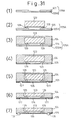
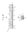
- Figure 35(1) shows an example of a semiconductor device according to the third aspect of the present invention including a capacitor.
- the illustrated semiconductor device 109 comprises, in addition to the structure of the semiconductor device 104' of Fig. 29(2), a capacitor 143 sealed in the resin member 124.
- the capacitor 143 has two electrode terminals 145 directly connected to the top surfaces of the metal interconnections 125.
- the capacitor 143 is a multilayer ceramic capacitor.
- the pattern surfaces of the inner electrodes 147 of the capacitor 143 are perpendicular to the thickness direction of the resin layer 124.
- the capacitor 143 is for example a normal ceramic multilayer capacitor.
- the spaces between the inner electrodes 147 are filled by a dielectric 149 such as strontium titanate.
- the electrostatic capacity that is, the effective area, is determined by the thickness after grinding and polishing, so it is necessary to estimate the final thickness in the design.
- capacitor 143 a commercially available capacitor such as a chip capacitor is suitably used.
- the structure including the capacitor 143 is not limited to the semiconductor device shown in Fig. 35(1) and can also be applied to the semiconductor devices shown in Figs. 24(1) and 24(2), Fig. 29(1), and Figs. 32(1) to 32(3).
- semiconductor devices that is, thin semiconductor packages, and processes of production thereof, which reduce and simultaneously achieve uniform mounting heights, do not require complicated steps for mounting individual chips, improve the manufacturing yield, achieve uniform heights of the semiconductor devices without being affected by variations in thickness of the chips, and enable electrical tests to be performed all at once.
Landscapes
- Encapsulation Of And Coatings For Semiconductor Or Solid State Devices (AREA)
- Wire Bonding (AREA)
- Structures Or Materials For Encapsulating Or Coating Semiconductor Devices Or Solid State Devices (AREA)
- Mechanical Treatment Of Semiconductor (AREA)
Abstract
Description
in either order, grinding and polishing to a predetermined thickness the top part of the sealing resin layer and the back surface portions of the semiconductor elements and patterning the metal substrate to form metal interconnections with top surfaces connected to the bottom ends of the connection terminals on the bottom surface of the resin member; and cutting the resin member into semiconductor package units to obtain individual semiconductor devices.
Claims (38)
- A semiconductor device provided with:an insulating tape substrate having through holes in the thickness direction;a semiconductor element mounted on a top surface of the tape substrate with its back surface exposed upward and its active surface facing downward;a sealing resin layer formed on the top surface of the tape substrate outside of the region in which the semiconductor device is mounted and sealing the area around the side surfaces of the semiconductor element;metal interconnections formed on the bottom surface of the tape substrate and blocking the bottom ends of the through holes of the tape substrate to define bottom portions;a solder resist layer covering the metal interconnections and the bottom surface of the tape substrate and having through holes in the thickness direction;external connection terminals projecting from the bottom surface of the metal interconnections and filling, passing through, and projecting out downward through the through holes of the solder resist layer;connection terminals extending downward from the active surface of the semiconductor element and inserted in the through holes of the tape substrate; anda filler comprised of a conductive material filling the gaps between the connection terminals and the inside walls of the through holes of the tape substrate and electrically connecting the connection terminals and the metal interconnections.
- A semiconductor device as set forth in claim 1, wherein the filler is formed using one of a low melting point metal and conductive paste.
- A semiconductor device as set forth in claim 1, further provided with conductor columns passing through said resin sealing layer and said tape substrate at a region where said resin sealing layer is formed, having top ends exposed at the top surface of the resin sealing layer, and having bottom ends electrically connected to said metal interconnection layer.
- A semiconductor device as set forth in claim 1, further provided with, instead of said sealing resin layer, an insulating frame bonded to the top surface of the tape substrate other than at the region where said semiconductor element is mounted and surrounding the side surfaces of said semiconductor element with a gap and a resin sealing layer filling said gap and sealing the area around the side surfaces of said semiconductor element and further provided with conductor columns passing through said frame and said tape substrate at a region where said frame is formed, having top ends exposed at the top surface of the frame, and having bottom ends electrically connected to said metal interconnection layer.
- A semiconductor device as set forth in claim 1, wherein the connection terminals extending downward from the active surface of the semiconductor element are bumps comprised of one of gold and copper.
- A semiconductor device as set forth in claim 1, wherein the external connection terminals filling and passing through the openings of the solder resist layer are arranged in one of a peripheral and area array mode.
- A semiconductor device as set forth in claim 1, wherein said filler is filled in the gap between said connection terminals and the through holes of said tape substrate up to a position of substantially the top ends of said through holes.
- A semiconductor device as set forth in claim 1, wherein the top surface of said sealing resin layer and the back surface of said semiconductor element form substantially the same plane.
- A multilayer semiconductor device comprised of a plurality of semiconductor devices as set forth in claim 3 or 4 stacked in layers, wherein the semiconductor devices of each layer are connected with each other at the top ends of the conductor columns and the bottom ends of the external connection terminals.
- A process of production of a semiconductor device comprising:forming through holes in the thickness direction in a tape substrate having an area able to accommodate a plurality of semiconductor package units and provided at its bottom surface with a metal interconnection layer and a solder resist layer and in said solder resist layer;filling a conductive material in the through holes of the tape substrate in amounts incompletely filling said through holes;inserting connection terminals of a number of semiconductor elements required for forming a plurality of semiconductor package units into the corresponding through holes of the tape substrate and filling the gaps between the connection terminals and the inside walls of the through holes by said conductive material until about the top ends of the through holes;bonding and mounting semiconductor elements on the top surface of the tape substrate;forming a sealing resin layer covering the top surface of the tape substrate other than the regions where the semiconductor elements are mounted and sealing the area around the side surfaces of the semiconductor element;grinding and polishing to a predetermined thickness the top part of the sealing resin layer and the back surface portions of the semiconductor elements; andcutting the tape substrate into semiconductor package units to obtain individual semiconductor devices.
- A process of production of a semiconductor device as set forth in claim 10, further comprising forming other through holes passing through the tape substrate at positions corresponding to conductor columns when forming through holes in the tape substrate and forming conductor columns filling said other through holes and projecting out from the top surface of said tape substrate before forming said sealing resin layer.
- A process of production of a semiconductor device as set forth in claim 10, further comprising bonding an insulating substrate provided with openings defining inner walls of frames to the top surface of said tape substrate, forming other through holes passing through the insulating substrate and the tape substrate at positions corresponding to conductor columns when forming through holes in the tape substrate, forming conductor columns filling said other through holes and projecting out from the top surface of said insulating substrate before mounting said semiconductor elements, and forming said sealing resin layer at the gaps after mounting the semiconductor elements.
- A process of production of a semiconductor device as set forth in claim 10, further comprising performing electrical tests after forming said sealing resin layer and one of before and after said grinding and said polishing.
- A process of production of a semiconductor device as set forth in claim 10, wherein the tape substrate able to accommodate said plurality of semiconductor package units is a disk shape.
- A semiconductor device provided with:an insulating tape substrate having metal interconnections on the top surface;a semiconductor element mounted on a top surface of said tape substrate with its back surface exposed upward and its active surface facing downward;a sealing resin layer formed on the top surface of the tape substrate, sealing the area around the side surfaces of the semiconductor element, and filling the gap between the active surface of the semiconductor element and the top surface of the tape substrate; andat least one ofconductor columns extending upward from the top surfaces of the metal interconnections, passing through the sealing resin layer at the area around the side surfaces of the semiconductor element, and having top ends exposed upward andexternal connection terminals extending downward from the bottom surfaces of the metal interconnection, passing through the tape substrate, and projecting downward.
- A semiconductor device as set forth in claim 15, wherein the top surface of said sealing resin layer and the back surface of said semiconductor element form substantially the same plane.
- A process of production of a semiconductor device comprising:preparing a tape substrate having an area able to accommodate a plurality of semiconductor package units and provided at its top surface with metal interconnections;bonding connection terminals of active surfaces of a number of semiconductor elements required for forming the plurality of semiconductor package units to the top surfaces of the metal interconnections of said tape substrate to mount said semiconductor elements on the top surface of said tape substrate;forming conductor columns with bottom ends bonded to the top surfaces of the metal interconnections;forming a sealing resin layer sealing the area around the side surfaces of the semiconductor elements, including said metal interconnections and conductor columns, and filling the gaps between the active surfaces of the semiconductor elements and the top surface of said tape substrate;grinding and polishing to a predetermined thickness the top part of the sealing resin layer and the back surface portions of the semiconductor elements and exposing the top ends of the conductor columns upward; andcutting the tape substrate into semiconductor package units to obtain individual semiconductor devices.
- A process of production of a semiconductor device comprising:preparing a tape substrate having an area able to accommodate a plurality of semiconductor package units, provided at its top surface with metal interconnections, having through holes in a thickness direction at positions corresponding to external connection terminals, and having bottom surfaces of said metal interconnections defining top ends of said through holes;bonding connection terminals of active surfaces of a number of semiconductor elements required for forming the plurality of semiconductor package units to the top surfaces of the metal interconnections of said tape substrate to mount said semiconductor elements on the top surface of said tape substrate;forming a sealing resin layer sealing the area around the side surfaces of the semiconductor elements, including said metal interconnections, and filling the gaps between the active surfaces of the semiconductor elements and the top surface of said tape substrate; then,in either order,grinding and polishing to a predetermined thickness the top part of the sealing resin layer and the back surface portions of the semiconductor elements andforming external connection terminals extending downward from the bottom surfaces of said metal interconnections defining the top ends of said through holes, filling said through holes, and projecting downward; andcutting the tape substrate into semiconductor package units to obtain individual semiconductor devices.
- A process of production of a semiconductor device comprising:preparing a tape substrate having an area able to accommodate a plurality of semiconductor package units, provided at its top surface with metal interconnections, having through holes in a thickness direction at positions corresponding to external connection terminals, and having bottom surfaces of said metal interconnections defining top ends of said through holes;bonding connection terminals of active surfaces of a number of semiconductor elements required for forming the plurality of semiconductor package units to the top surface of the metal interconnections of said tape substrate to mount said semiconductor elements on the top surface of said tape substrate;forming conductor columns with bottom ends bonded to the top surfaces of the metal interconnections;forming a sealing resin layer sealing the area around the side surfaces of the semiconductor elements, including said metal interconnections and conductor columns, and filling the gaps between the active surfaces of the semiconductor elements and the top surface of said tape substrate; then,in either order,grinding and polishing to a predetermined thickness the top part of the sealing resin layer and the back surface portions of the semiconductor elements and exposing the top ends of the conductor columns upward andforming external connection terminals extending downward from the bottom surfaces of said metal interconnections defining the top ends of said through holes, filling said through holes, and projecting downward; andcutting the tape substrate into semiconductor package units to obtain individual semiconductor devices.
- A semiconductor device provided with:a resin member of a predetermined thickness;a semiconductor element sealed inside said resin member, having a back surface exposed at a top surface of said resin member, and having an active surface facing downward;metal interconnections formed on the bottom surface of the resin member; andconnection terminals extending downward from the active surface of the semiconductor element and having bottom ends connected to top surfaces of said metal interconnections.
- A semiconductor device as set forth in claim 20, wherein the top surface of said sealing resin layer and the back surface of said semiconductor element form substantially the same plane.
- A semiconductor device as set forth in claim 20, further provided with a solder resist layer covering the entire bottom surface of said resin member including said metal interconnections and connection bumps formed on the bottom surfaces of said metal interconnections, passing through said solder resist layer, and projecting downward.
- A semiconductor device as set forth in claim 20, further provided with a plurality of conductor columns passing through said resin member from the top surfaces of said metal interconnections, extending upward, and having top ends exposed at the top surface of said resin member.
- A semiconductor device as set forth in claim 23, wherein the side surfaces of the conductor columns are exposed at the side surfaces of the resin member.
- A semiconductor device as set forth in claim 20, further provided with a capacitor sealed inside said resin member and directly connected with said metal interconnections.
- A semiconductor device as set forth in claim 25, wherein said capacitor is a multilayer ceramic capacitor including inner electrodes each having a surface being perpendicular to the thickness direction of said resin member.
- A semiconductor device as set forth in claim 20, wherein an inorganic filler is dispersed in said resin member.
- A multilayer semiconductor device comprised of a plurality of semiconductor devices as set forth in claim 23 stacked in layers, wherein the semiconductor devices of each layer are connected with each other at the top ends of the conductor columns and the bottom ends of the metal interconnections through connection bumps.
- A parallel semiconductor device comprised of a plurality of semiconductor devices as set forth in claim 24 connected to each other at their side surfaces, wherein the semiconductor devices adjoining each other at their sides are electrically connected with each other at the side surfaces of the conductor columns exposed at the side surfaces of said resin member.
- A multilayer parallel semiconductor device comprised of a plurality of semiconductor devices as set forth in claim 24 stacked in layers and connected to each other at their side surfaces, wherein the semiconductor devices of each layer are electrically connected with each other at the top ends of the conductor columns and the bottom ends of the metal interconnections through connection bumps and wherein the semiconductor devices adjoining each other at their sides are electrically connected with each other at the side surfaces of the conductor columns exposed at the side surfaces of said resin member.
- A process of production of a semiconductor device comprising:mounting on the top surface of a metal substrate having an area able to accommodate a plurality of semiconductor package units semiconductor elements by turning the active surfaces of semiconductor elements downward and bonding front ends of connection terminals to the metal substrate;covering the entire top surface of the metal substrate by a resin to form a resin member in which the semiconductor elements are sealed and to the bottom surface of which said metal substrate is bonded; then,in either order,grinding and polishing to a predetermined thickness the top part of the sealing resin layer and the back surface portions of the semiconductor elements andpatterning the metal substrate to form metal interconnections with top surfaces connected to the bottom ends of said connection terminals on the bottom surface of said resin member; andcutting the resin member into semiconductor package units to obtain individual semiconductor devices.
- A process of production of a semiconductor device as set forth in claim 31, further comprising forming conductor columns on the top surface of said metal substrate after forming said semiconductor elements on said metal substrate and before forming said resin member.
- A process of production of a semiconductor device as set forth in claim 32, wherein said conductor columns are formed so that at least one of said top ends and side surfaces are exposed from said resin member.
- A process of production of a semiconductor device as set forth in claim 31, further comprising, after forming the metal interconnections on the bottom surface of said resin member, forming a solder resist layer covering the entire bottom surface of said resin member, including said metal interconnections, and connection bumps formed on the bottom surfaces of said metal interconnections, passing through the solder resist layer, and projecting downward.
- A process of production of a semiconductor device comprising:preparing a composite metal plate comprised of a metal substrate having an area able to accommodate a plurality of semiconductor package units and of an interconnection pattern comprised of a different type of metal from said metal substrate on its top surface;mounting semiconductor elements on the top surface of the composite metal plate by turning the active surfaces of semiconductor elements downward and bonding front ends of connection terminals to the composite metal plate;covering the entire top surface of the composite metal plate by a resin to form a resin member in which the semiconductor elements are sealed and to the bottom surface of which said composite metal plate is bonded; then,in either order,grinding and polishing to a predetermined thickness the top part of the resin member and the back surface portions of the semiconductor elements andetching away the metal substrate of said composite metal plate and leaving the interconnection pattern so as to form metal interconnections comprised of said interconnection pattern with top surfaces connected to the bottom ends of said connection terminals on the bottom surface of the resin member; andcutting the resin member into semiconductor package units to obtain individual semiconductor devices.
- A process of production of a semiconductor device as set forth in claim 35, further comprising forming conductor columns on the top surface of said metal substrate after forming said semiconductor elements on said composite metal plate and before forming said resin member.
- A process of production of a semiconductor device as set forth in claim 36, wherein said conductor columns are formed so that at least one of said top ends and side surfaces are exposed from said resin member.
- A process of production of a semiconductor device as set forth in claim 35, further comprising, after forming the metal interconnections on the bottom surface of said resin member, forming a solder resist layer covering the entire bottom surface of said resin member, including said metal interconnections, and connection bumps formed on the bottom surfaces of said metal interconnections, passing through the solder resist layer, and projecting downward.
Applications Claiming Priority (4)
| Application Number | Priority Date | Filing Date | Title |
|---|---|---|---|
| JP2000088593 | 2000-03-24 | ||
| JP2000088593 | 2000-03-24 | ||
| JP2000252846A JP2001339011A (en) | 2000-03-24 | 2000-08-23 | Semiconductor device and method of manufacturing the same |
| JP2000252846 | 2000-08-23 |
Publications (2)
| Publication Number | Publication Date |
|---|---|
| EP1137066A2 true EP1137066A2 (en) | 2001-09-26 |
| EP1137066A3 EP1137066A3 (en) | 2004-12-22 |
Family
ID=26588557
Family Applications (1)
| Application Number | Title | Priority Date | Filing Date |
|---|---|---|---|
| EP01106434A Withdrawn EP1137066A3 (en) | 2000-03-24 | 2001-03-22 | Semiconductor device and process of production of same |
Country Status (5)
| Country | Link |
|---|---|
| US (1) | US6774467B2 (en) |
| EP (1) | EP1137066A3 (en) |
| JP (1) | JP2001339011A (en) |
| KR (1) | KR20010090540A (en) |
| TW (1) | TW504804B (en) |
Cited By (15)
| Publication number | Priority date | Publication date | Assignee | Title |
|---|---|---|---|---|
| WO2003067648A3 (en) * | 2002-02-04 | 2003-10-30 | Casio Computer Co Ltd | Semiconductor device and method of manufacturing the same |
| EP1418617A3 (en) * | 2002-11-05 | 2004-05-26 | Shinko Electric Co. Ltd. | Semiconductor device and method of manufacturing the same |
| WO2004105134A1 (en) * | 2003-05-20 | 2004-12-02 | Infineon Technologies Ag | An integrated circuit package |
| FR2857156A1 (en) * | 2003-07-03 | 2005-01-07 | Temex Sa | METHOD FOR MANUFACTURING ELECTRONIC COMPONENTS OF REDUCED THICKNESS |
| WO2005004237A1 (en) * | 2003-07-01 | 2005-01-13 | 3D Plus | Method for interconnecting active and passive components, and a resulting thin heterogeneous component |
| EP1168441A3 (en) * | 2000-06-23 | 2005-06-15 | Shinko Electric Industries Co. Ltd. | Multi-layer wiring substrate and semiconductor device using the multi-layer wiring substrate |
| WO2005041295A3 (en) * | 2003-10-15 | 2005-06-16 | Infineon Technologies Ag | Semiconductor module provided with contacts extending through the housing |
| FR2894070A1 (en) * | 2005-11-30 | 2007-06-01 | 3D Plus Sa Sa | 3D ELECTRONIC MODULE |
| CN100461391C (en) * | 2002-02-04 | 2009-02-11 | 卡西欧计算机株式会社 | Semiconductor device |
| WO2008111546A3 (en) * | 2007-03-09 | 2009-05-22 | Casio Computer Co Ltd | Semiconductor device having semiconductor structure bodies on upper and lower surfaces thereof, and method of manufacturing the same |
| US7618886B2 (en) | 2002-08-09 | 2009-11-17 | Casio Computer Co., Ltd. | Semiconductor device and method of manufacturing the same |
| WO2016044389A1 (en) * | 2014-09-16 | 2016-03-24 | Invensas Corporation | Use of underfill tape in microelectronic components, and microelectronic components with cavities coupled to through-substrate vias |
| DE102016203453A1 (en) * | 2016-03-02 | 2017-09-07 | Fraunhofer-Gesellschaft zur Förderung der angewandten Forschung e.V. | Method for producing a semiconductor component and semiconductor component |
| US10743422B2 (en) | 2016-09-27 | 2020-08-11 | At&S Austria Technologie & Systemtechnik Aktiengesellschaft | Embedding a component in a core on conductive foil |
| CN113039655A (en) * | 2018-11-08 | 2021-06-25 | Lg伊诺特有限公司 | Thermoelectric module |
Families Citing this family (143)
| Publication number | Priority date | Publication date | Assignee | Title |
|---|---|---|---|---|
| JP3339838B2 (en) | 1999-06-07 | 2002-10-28 | ローム株式会社 | Semiconductor device and method of manufacturing the same |
| US10388626B2 (en) * | 2000-03-10 | 2019-08-20 | STATS ChipPAC Pte. Ltd. | Semiconductor device and method of forming flipchip interconnect structure |
| EP1278612B1 (en) * | 2000-03-10 | 2010-02-24 | Chippac, Inc. | Flip chip Interconnection structure and method of obtaining the same |
| US7094676B1 (en) | 2000-10-13 | 2006-08-22 | Bridge Semiconductor Corporation | Semiconductor chip assembly with embedded metal pillar |
| US7190080B1 (en) * | 2000-10-13 | 2007-03-13 | Bridge Semiconductor Corporation | Semiconductor chip assembly with embedded metal pillar |
| JP2002134650A (en) * | 2000-10-23 | 2002-05-10 | Rohm Co Ltd | Semiconductor device and manufacturing method thereof |
| JP3420748B2 (en) | 2000-12-14 | 2003-06-30 | 松下電器産業株式会社 | Semiconductor device and manufacturing method thereof |
| TW511405B (en) * | 2000-12-27 | 2002-11-21 | Matsushita Electric Industrial Co Ltd | Device built-in module and manufacturing method thereof |
| JP2008118152A (en) * | 2001-03-26 | 2008-05-22 | Nec Electronics Corp | Semiconductor device and stacked semiconductor device |
| US7034386B2 (en) | 2001-03-26 | 2006-04-25 | Nec Corporation | Thin planar semiconductor device having electrodes on both surfaces and method of fabricating same |
| JP4248761B2 (en) * | 2001-04-27 | 2009-04-02 | 新光電気工業株式会社 | Semiconductor package, manufacturing method thereof, and semiconductor device |
| US6838750B2 (en) * | 2001-07-12 | 2005-01-04 | Custom One Design, Inc. | Interconnect circuitry, multichip module, and methods of manufacturing thereof |
| JP4023159B2 (en) * | 2001-07-31 | 2007-12-19 | ソニー株式会社 | Manufacturing method of semiconductor device and manufacturing method of laminated semiconductor device |
| US7297572B2 (en) * | 2001-09-07 | 2007-11-20 | Hynix Semiconductor, Inc. | Fabrication method for electronic system modules |
| US6927471B2 (en) * | 2001-09-07 | 2005-08-09 | Peter C. Salmon | Electronic system modules and method of fabrication |
| TW544882B (en) | 2001-12-31 | 2003-08-01 | Megic Corp | Chip package structure and process thereof |
| TW584950B (en) | 2001-12-31 | 2004-04-21 | Megic Corp | Chip packaging structure and process thereof |
| US6673698B1 (en) | 2002-01-19 | 2004-01-06 | Megic Corporation | Thin film semiconductor package utilizing a glass substrate with composite polymer/metal interconnect layers |
| TW503496B (en) | 2001-12-31 | 2002-09-21 | Megic Corp | Chip packaging structure and manufacturing process of the same |
| US6763580B2 (en) * | 2002-03-21 | 2004-07-20 | Motorola, Inc. | Method and apparatus for securing an electrically conductive interconnect through a metallic substrate |
| JP4107643B2 (en) * | 2002-07-23 | 2008-06-25 | 日本碍子株式会社 | Manufacturing method of joined body |
| US6964881B2 (en) * | 2002-08-27 | 2005-11-15 | Micron Technology, Inc. | Multi-chip wafer level system packages and methods of forming same |
| US6786391B2 (en) * | 2002-10-16 | 2004-09-07 | Kac Holdings, Inc. | Method of controlling solder deposition utilizing two fluxes and preform |
| US7388294B2 (en) * | 2003-01-27 | 2008-06-17 | Micron Technology, Inc. | Semiconductor components having stacked dice |
| JP3891123B2 (en) * | 2003-02-06 | 2007-03-14 | セイコーエプソン株式会社 | SEMICONDUCTOR DEVICE, ELECTRONIC DEVICE, ELECTRONIC DEVICE, AND SEMICONDUCTOR DEVICE MANUFACTURING METHOD |
| JP4052955B2 (en) | 2003-02-06 | 2008-02-27 | Necエレクトロニクス株式会社 | Manufacturing method of semiconductor device |
| JP4110992B2 (en) * | 2003-02-07 | 2008-07-02 | セイコーエプソン株式会社 | Semiconductor device, electronic device, electronic apparatus, semiconductor device manufacturing method, and electronic device manufacturing method |
| JP2004281818A (en) * | 2003-03-17 | 2004-10-07 | Seiko Epson Corp | Semiconductor device, electronic device, electronic device, method of manufacturing carrier substrate, method of manufacturing semiconductor device, and method of manufacturing electronic device |
| JP4069771B2 (en) * | 2003-03-17 | 2008-04-02 | セイコーエプソン株式会社 | SEMICONDUCTOR DEVICE, ELECTRONIC DEVICE, AND SEMICONDUCTOR DEVICE MANUFACTURING METHOD |
| JP2004281920A (en) * | 2003-03-18 | 2004-10-07 | Seiko Epson Corp | Semiconductor device, electronic device, electronic equipment, method of manufacturing semiconductor device, and method of manufacturing electronic device |
| JP2004281919A (en) * | 2003-03-18 | 2004-10-07 | Seiko Epson Corp | Semiconductor device, electronic device, electronic equipment, method of manufacturing semiconductor device, and method of manufacturing electronic device |
| JP4096774B2 (en) * | 2003-03-24 | 2008-06-04 | セイコーエプソン株式会社 | SEMICONDUCTOR DEVICE, ELECTRONIC DEVICE, ELECTRONIC DEVICE, SEMICONDUCTOR DEVICE MANUFACTURING METHOD, AND ELECTRONIC DEVICE MANUFACTURING METHOD |
| JP2004349495A (en) * | 2003-03-25 | 2004-12-09 | Seiko Epson Corp | Semiconductor device, electronic device, electronic apparatus, and method of manufacturing semiconductor device |
| JP3972846B2 (en) | 2003-03-25 | 2007-09-05 | セイコーエプソン株式会社 | Manufacturing method of semiconductor device |
| JP3574450B1 (en) | 2003-05-16 | 2004-10-06 | 沖電気工業株式会社 | Semiconductor device and method of manufacturing semiconductor device |
| JP3646720B2 (en) * | 2003-06-19 | 2005-05-11 | セイコーエプソン株式会社 | Semiconductor device and manufacturing method thereof, circuit board, and electronic apparatus |
| KR100493063B1 (en) * | 2003-07-18 | 2005-06-02 | 삼성전자주식회사 | BGA package with stacked semiconductor chips and manufacturing method thereof |
| JP4271590B2 (en) * | 2004-01-20 | 2009-06-03 | 新光電気工業株式会社 | Semiconductor device and manufacturing method thereof |
| JP4434845B2 (en) * | 2004-06-08 | 2010-03-17 | 三洋電機株式会社 | Semiconductor module, method for manufacturing the same, and semiconductor device |
| KR100568496B1 (en) * | 2004-10-21 | 2006-04-07 | 삼성전자주식회사 | Film Circuit Board with Tin-Indium Alloy Layer |
| JP5592055B2 (en) | 2004-11-03 | 2014-09-17 | テッセラ,インコーポレイテッド | Improved stacking packaging |
| JP4990492B2 (en) * | 2004-11-19 | 2012-08-01 | 株式会社テラミクロス | Semiconductor device |
| JP4444088B2 (en) * | 2004-12-10 | 2010-03-31 | 新光電気工業株式会社 | Semiconductor device |
| CN101138088B (en) * | 2005-03-09 | 2010-10-06 | 松下电器产业株式会社 | Die mounting structure and die mounting method |
| US7589407B2 (en) * | 2005-04-11 | 2009-09-15 | Stats Chippac Ltd. | Semiconductor multipackage module including tape substrate land grid array package stacked over ball grid array package |
| US7675152B2 (en) * | 2005-09-01 | 2010-03-09 | Texas Instruments Incorporated | Package-on-package semiconductor assembly |
| US20070051774A1 (en) * | 2005-09-06 | 2007-03-08 | Stipp John N | Method of controlling solder deposition on heat spreader used for semiconductor package |
| US7947535B2 (en) * | 2005-10-22 | 2011-05-24 | Stats Chippac Ltd. | Thin package system with external terminals |
| US8058101B2 (en) | 2005-12-23 | 2011-11-15 | Tessera, Inc. | Microelectronic packages and methods therefor |
| US7569422B2 (en) | 2006-08-11 | 2009-08-04 | Megica Corporation | Chip package and method for fabricating the same |
| KR100966194B1 (en) * | 2006-09-26 | 2010-06-25 | 가부시끼가이샤 도시바 | Ultrasonic transducer |
| JP5394604B2 (en) * | 2006-09-29 | 2014-01-22 | 新光電気工業株式会社 | Semiconductor device and manufacturing method thereof |
| US7898093B1 (en) | 2006-11-02 | 2011-03-01 | Amkor Technology, Inc. | Exposed die overmolded flip chip package and fabrication method |
| JP4758869B2 (en) * | 2006-11-08 | 2011-08-31 | 新光電気工業株式会社 | Manufacturing method of semiconductor device |
| JP2008235401A (en) * | 2007-03-19 | 2008-10-02 | Spansion Llc | Semiconductor device and manufacturing method thereof |
| JP5273956B2 (en) * | 2007-07-02 | 2013-08-28 | スパンション エルエルシー | Manufacturing method of semiconductor device |
| JP5215605B2 (en) * | 2007-07-17 | 2013-06-19 | ラピスセミコンダクタ株式会社 | Manufacturing method of semiconductor device |
| JP5081578B2 (en) * | 2007-10-25 | 2012-11-28 | ローム株式会社 | Resin-sealed semiconductor device |
| FR2923081B1 (en) * | 2007-10-26 | 2009-12-11 | 3D Plus | PROCESS FOR VERTICAL INTERCONNECTION OF 3D ELECTRONIC MODULES BY VIAS. |
| US8390117B2 (en) * | 2007-12-11 | 2013-03-05 | Panasonic Corporation | Semiconductor device and method of manufacturing the same |
| US8063474B2 (en) * | 2008-02-06 | 2011-11-22 | Fairchild Semiconductor Corporation | Embedded die package on package (POP) with pre-molded leadframe |
| CN101599474B (en) * | 2008-06-02 | 2011-04-13 | 相丰科技股份有限公司 | Integrated circuit module and manufacturing method thereof |
| TWI489599B (en) * | 2008-06-02 | 2015-06-21 | 相豐科技股份有限公司 | Integrated circuit module and manufacturing method thereof |
| JP4489821B2 (en) * | 2008-07-02 | 2010-06-23 | 新光電気工業株式会社 | Semiconductor device and manufacturing method thereof |
| FI125526B (en) * | 2008-08-25 | 2015-11-13 | Ge Embedded Electronics Oy | Packaged circuit board assembly containing electrical components and method of manufacturing a packaged circuit board assembly including electrical components |
| US7855439B2 (en) * | 2008-08-28 | 2010-12-21 | Fairchild Semiconductor Corporation | Molded ultra thin semiconductor die packages, systems using the same, and methods of making the same |
| JP5179391B2 (en) | 2009-01-23 | 2013-04-10 | 新光電気工業株式会社 | Semiconductor device manufacturing method and semiconductor device |
| US8163597B2 (en) * | 2009-03-24 | 2012-04-24 | Stats Chippac, Ltd. | Semiconductor device and method of forming no-flow underfill material around vertical interconnect structure |
| US8531015B2 (en) * | 2009-03-26 | 2013-09-10 | Stats Chippac, Ltd. | Semiconductor device and method of forming a thin wafer without a carrier |
| JP4877365B2 (en) * | 2009-07-13 | 2012-02-15 | 日立化成工業株式会社 | Circuit connection method |
| US9064716B2 (en) * | 2009-09-30 | 2015-06-23 | Virtium Technology, Inc. | Stacking devices at finished package level |
| US8304286B2 (en) * | 2009-12-11 | 2012-11-06 | Stats Chippac Ltd. | Integrated circuit packaging system with shielded package and method of manufacture thereof |
| US8884422B2 (en) * | 2009-12-31 | 2014-11-11 | Stmicroelectronics Pte Ltd. | Flip-chip fan-out wafer level package for package-on-package applications, and method of manufacture |
| KR101633398B1 (en) * | 2010-02-16 | 2016-06-24 | 삼성전자주식회사 | A land grid array package capable of decreasing a height difference between land and solder resist |
| US8482111B2 (en) | 2010-07-19 | 2013-07-09 | Tessera, Inc. | Stackable molded microelectronic packages |
| US9159708B2 (en) | 2010-07-19 | 2015-10-13 | Tessera, Inc. | Stackable molded microelectronic packages with area array unit connectors |
| TWI435397B (en) * | 2010-08-06 | 2014-04-21 | 國立交通大學 | Soft micro system structure and manufacturing method thereof |
| KR101677739B1 (en) * | 2010-09-29 | 2016-11-21 | 삼성전자주식회사 | package for semiconductor device and manufacturing method of the same |
| KR101075241B1 (en) | 2010-11-15 | 2011-11-01 | 테세라, 인코포레이티드 | Microelectronic package with terminals in dielectric member |
| JP2012114173A (en) * | 2010-11-23 | 2012-06-14 | Shinko Electric Ind Co Ltd | Manufacturing method of semiconductor device and the semiconductor device |
| US20120146206A1 (en) | 2010-12-13 | 2012-06-14 | Tessera Research Llc | Pin attachment |
| KR101128063B1 (en) | 2011-05-03 | 2012-04-23 | 테세라, 인코포레이티드 | Package-on-package assembly with wire bonds to encapsulation surface |
| US8618659B2 (en) | 2011-05-03 | 2013-12-31 | Tessera, Inc. | Package-on-package assembly with wire bonds to encapsulation surface |
| US9064883B2 (en) | 2011-08-25 | 2015-06-23 | Intel Mobile Communications GmbH | Chip with encapsulated sides and exposed surface |
| US9013037B2 (en) | 2011-09-14 | 2015-04-21 | Stmicroelectronics Pte Ltd. | Semiconductor package with improved pillar bump process and structure |
| US9105483B2 (en) | 2011-10-17 | 2015-08-11 | Invensas Corporation | Package-on-package assembly with wire bond vias |
| US8779601B2 (en) | 2011-11-02 | 2014-07-15 | Stmicroelectronics Pte Ltd | Embedded wafer level package for 3D and package-on-package applications, and method of manufacture |
| US8916481B2 (en) | 2011-11-02 | 2014-12-23 | Stmicroelectronics Pte Ltd. | Embedded wafer level package for 3D and package-on-package applications, and method of manufacture |
| JP2013110264A (en) * | 2011-11-21 | 2013-06-06 | Fujitsu Semiconductor Ltd | Semiconductor device and semiconductor device manufacturing method |
| KR20130089473A (en) * | 2012-02-02 | 2013-08-12 | 삼성전자주식회사 | Semiconductor package |
| US8946757B2 (en) | 2012-02-17 | 2015-02-03 | Invensas Corporation | Heat spreading substrate with embedded interconnects |
| US8372741B1 (en) | 2012-02-24 | 2013-02-12 | Invensas Corporation | Method for package-on-package assembly with wire bonds to encapsulation surface |
| US9349706B2 (en) | 2012-02-24 | 2016-05-24 | Invensas Corporation | Method for package-on-package assembly with wire bonds to encapsulation surface |
| US8901730B2 (en) | 2012-05-03 | 2014-12-02 | Taiwan Semiconductor Manufacturing Company, Ltd. | Methods and apparatus for package on package devices |
| US8835228B2 (en) | 2012-05-22 | 2014-09-16 | Invensas Corporation | Substrate-less stackable package with wire-bond interconnect |
| US9349663B2 (en) | 2012-06-29 | 2016-05-24 | Taiwan Semiconductor Manufacturing Co., Ltd. | Package-on-package structure having polymer-based material for warpage control |
| JP5961055B2 (en) * | 2012-07-05 | 2016-08-02 | 日東電工株式会社 | Sealing resin sheet, electronic component package manufacturing method, and electronic component package |
| US9391008B2 (en) | 2012-07-31 | 2016-07-12 | Invensas Corporation | Reconstituted wafer-level package DRAM |
| US9502390B2 (en) | 2012-08-03 | 2016-11-22 | Invensas Corporation | BVA interposer |
| KR20140048468A (en) * | 2012-10-15 | 2014-04-24 | 삼성전자주식회사 | A pakage substrate and semiconductor pakage including the same |
| US8975738B2 (en) | 2012-11-12 | 2015-03-10 | Invensas Corporation | Structure for microelectronic packaging with terminals on dielectric mass |
| US8878353B2 (en) | 2012-12-20 | 2014-11-04 | Invensas Corporation | Structure for microelectronic packaging with bond elements to encapsulation surface |
| US9136254B2 (en) | 2013-02-01 | 2015-09-15 | Invensas Corporation | Microelectronic package having wire bond vias and stiffening layer |
| JP2014165339A (en) * | 2013-02-25 | 2014-09-08 | Disco Abrasive Syst Ltd | Method of processing laminated wafer |
| JP6084114B2 (en) * | 2013-05-10 | 2017-02-22 | 株式会社ディスコ | Processing method of package substrate |
| US8883563B1 (en) | 2013-07-15 | 2014-11-11 | Invensas Corporation | Fabrication of microelectronic assemblies having stack terminals coupled by connectors extending through encapsulation |
| US9034696B2 (en) | 2013-07-15 | 2015-05-19 | Invensas Corporation | Microelectronic assemblies having reinforcing collars on connectors extending through encapsulation |
| US9023691B2 (en) | 2013-07-15 | 2015-05-05 | Invensas Corporation | Microelectronic assemblies with stack terminals coupled by connectors extending through encapsulation |
| US9167710B2 (en) | 2013-08-07 | 2015-10-20 | Invensas Corporation | Embedded packaging with preformed vias |
| US9685365B2 (en) | 2013-08-08 | 2017-06-20 | Invensas Corporation | Method of forming a wire bond having a free end |
| US20150076714A1 (en) | 2013-09-16 | 2015-03-19 | Invensas Corporation | Microelectronic element with bond elements to encapsulation surface |
| US9087815B2 (en) | 2013-11-12 | 2015-07-21 | Invensas Corporation | Off substrate kinking of bond wire |
| US9082753B2 (en) | 2013-11-12 | 2015-07-14 | Invensas Corporation | Severing bond wire by kinking and twisting |
| US9379074B2 (en) | 2013-11-22 | 2016-06-28 | Invensas Corporation | Die stacks with one or more bond via arrays of wire bond wires and with one or more arrays of bump interconnects |
| US9263394B2 (en) | 2013-11-22 | 2016-02-16 | Invensas Corporation | Multiple bond via arrays of different wire heights on a same substrate |
| US9583456B2 (en) | 2013-11-22 | 2017-02-28 | Invensas Corporation | Multiple bond via arrays of different wire heights on a same substrate |
| US9559064B2 (en) | 2013-12-04 | 2017-01-31 | Taiwan Semiconductor Manufacturing Company, Ltd. | Warpage control in package-on-package structures |
| US9583411B2 (en) | 2014-01-17 | 2017-02-28 | Invensas Corporation | Fine pitch BVA using reconstituted wafer with area array accessible for testing |
| US9711485B1 (en) | 2014-02-04 | 2017-07-18 | Amkor Technology, Inc. | Thin bonded interposer package |
| US9214454B2 (en) | 2014-03-31 | 2015-12-15 | Invensas Corporation | Batch process fabrication of package-on-package microelectronic assemblies |
| US10381326B2 (en) | 2014-05-28 | 2019-08-13 | Invensas Corporation | Structure and method for integrated circuits packaging with increased density |
| US9646917B2 (en) | 2014-05-29 | 2017-05-09 | Invensas Corporation | Low CTE component with wire bond interconnects |
| US9412714B2 (en) | 2014-05-30 | 2016-08-09 | Invensas Corporation | Wire bond support structure and microelectronic package including wire bonds therefrom |
| TWI660476B (en) * | 2014-07-11 | 2019-05-21 | Siliconware Precision Industries Co., Ltd. | Package structure and method of manufacture |
| US9735084B2 (en) | 2014-12-11 | 2017-08-15 | Invensas Corporation | Bond via array for thermal conductivity |
| US9888579B2 (en) | 2015-03-05 | 2018-02-06 | Invensas Corporation | Pressing of wire bond wire tips to provide bent-over tips |
| US9786623B2 (en) * | 2015-03-17 | 2017-10-10 | STATS ChipPAC Pte. Ltd. | Semiconductor device and method of forming PoP semiconductor device with RDL over top package |
| US9530749B2 (en) | 2015-04-28 | 2016-12-27 | Invensas Corporation | Coupling of side surface contacts to a circuit platform |
| US9502372B1 (en) | 2015-04-30 | 2016-11-22 | Invensas Corporation | Wafer-level packaging using wire bond wires in place of a redistribution layer |
| US9761554B2 (en) | 2015-05-07 | 2017-09-12 | Invensas Corporation | Ball bonding metal wire bond wires to metal pads |
| US10490528B2 (en) | 2015-10-12 | 2019-11-26 | Invensas Corporation | Embedded wire bond wires |
| US9490222B1 (en) | 2015-10-12 | 2016-11-08 | Invensas Corporation | Wire bond wires for interference shielding |
| US10332854B2 (en) | 2015-10-23 | 2019-06-25 | Invensas Corporation | Anchoring structure of fine pitch bva |
| US10181457B2 (en) | 2015-10-26 | 2019-01-15 | Invensas Corporation | Microelectronic package for wafer-level chip scale packaging with fan-out |
| US9911718B2 (en) | 2015-11-17 | 2018-03-06 | Invensas Corporation | ‘RDL-First’ packaged microelectronic device for a package-on-package device |
| US9659848B1 (en) | 2015-11-18 | 2017-05-23 | Invensas Corporation | Stiffened wires for offset BVA |
| US9984992B2 (en) | 2015-12-30 | 2018-05-29 | Invensas Corporation | Embedded wire bond wires for vertical integration with separate surface mount and wire bond mounting surfaces |
| US9935075B2 (en) | 2016-07-29 | 2018-04-03 | Invensas Corporation | Wire bonding method and apparatus for electromagnetic interference shielding |
| US10299368B2 (en) | 2016-12-21 | 2019-05-21 | Invensas Corporation | Surface integrated waveguides and circuit structures therefor |
| JP6850336B1 (en) * | 2019-12-05 | 2021-03-31 | ソフトバンク株式会社 | Three-dimensional laminated integrated circuit using immersion cooling method using semiconductor package and perforated interposer |
| JP2023147595A (en) * | 2022-03-30 | 2023-10-13 | 浜松ホトニクス株式会社 | Manufacturing method of optical semiconductor package |
| US20250201662A1 (en) * | 2023-12-13 | 2025-06-19 | Qualcomm Incorporated | Integrated circuit device including thermal interposer layer |
| CN118471938B (en) * | 2024-06-26 | 2025-02-11 | 池州昀钐半导体材料有限公司 | Lead frame and package assembly |
Family Cites Families (25)
| Publication number | Priority date | Publication date | Assignee | Title |
|---|---|---|---|---|
| JP2840316B2 (en) * | 1989-09-06 | 1998-12-24 | 新光電気工業株式会社 | Semiconductor device and manufacturing method thereof |
| KR100238197B1 (en) * | 1992-12-15 | 2000-01-15 | 윤종용 | Semiconductor device |
| US5353498A (en) | 1993-02-08 | 1994-10-11 | General Electric Company | Method for fabricating an integrated circuit module |
| JPH06268101A (en) * | 1993-03-17 | 1994-09-22 | Hitachi Ltd | Semiconductor device and manufacturing method thereof, electronic device, lead frame and mounting substrate |
| EP1213755A3 (en) * | 1994-03-18 | 2005-05-25 | Hitachi Chemical Co., Ltd. | Fabrication process of semiconductor package and semiconductor package |
| JP2595909B2 (en) * | 1994-09-14 | 1997-04-02 | 日本電気株式会社 | Semiconductor device |
| JP3400877B2 (en) * | 1994-12-14 | 2003-04-28 | 三菱電機株式会社 | Semiconductor device and manufacturing method thereof |
| JP2944449B2 (en) * | 1995-02-24 | 1999-09-06 | 日本電気株式会社 | Semiconductor package and manufacturing method thereof |
| JPH08335653A (en) * | 1995-04-07 | 1996-12-17 | Nitto Denko Corp | SEMICONDUCTOR DEVICE, METHOD FOR MANUFACTURING THE SAME, AND TAPE CARRIER FOR SEMICONDUCTOR DEVICE USED IN MANUFACTURING THE SEMICONDUCTOR DEVICE |
| JPH08288424A (en) * | 1995-04-18 | 1996-11-01 | Nec Corp | Semiconductor device |
| US5668409A (en) * | 1995-06-05 | 1997-09-16 | Harris Corporation | Integrated circuit with edge connections and method |
| US5832600A (en) * | 1995-06-06 | 1998-11-10 | Seiko Epson Corporation | Method of mounting electronic parts |
| JP2899540B2 (en) * | 1995-06-12 | 1999-06-02 | 日東電工株式会社 | Film carrier and semiconductor device using the same |
| US6022761A (en) * | 1996-05-28 | 2000-02-08 | Motorola, Inc. | Method for coupling substrates and structure |
| JP3610999B2 (en) * | 1996-06-07 | 2005-01-19 | 松下電器産業株式会社 | Mounting method of semiconductor element |
| EP1271640A3 (en) * | 1996-07-12 | 2003-07-16 | Fujitsu Limited | Mold for manufacturing semiconductor device |
| US5848466A (en) * | 1996-11-19 | 1998-12-15 | Motorola, Inc. | Method for forming a microelectronic assembly |
| JP3793628B2 (en) * | 1997-01-20 | 2006-07-05 | 沖電気工業株式会社 | Resin-sealed semiconductor device |
| JPH10242333A (en) * | 1997-03-01 | 1998-09-11 | Nitto Denko Corp | Semiconductor device and method of manufacturing semiconductor device |
| JPH10294423A (en) * | 1997-04-17 | 1998-11-04 | Nec Corp | Semiconductor device |
| JPH1167979A (en) * | 1997-08-13 | 1999-03-09 | Citizen Watch Co Ltd | Mounting structure of flip chip semiconductor package and method of manufacturing the same |
| US6038133A (en) * | 1997-11-25 | 2000-03-14 | Matsushita Electric Industrial Co., Ltd. | Circuit component built-in module and method for producing the same |
| JPH11260863A (en) * | 1998-03-09 | 1999-09-24 | Sumitomo Electric Ind Ltd | Connection terminal for semiconductor device and manufacturing method thereof |
| US20020149027A1 (en) * | 1998-03-19 | 2002-10-17 | Noriyuki Takahashi | Semiconductor device and its manufacture, and semiconductor device packaging structure |
| US7129110B1 (en) * | 1999-08-23 | 2006-10-31 | Rohm Co., Ltd. | Semiconductor device and method for manufacturing the same |
-
2000
- 2000-08-23 JP JP2000252846A patent/JP2001339011A/en active Pending
-
2001
- 2001-03-20 US US09/812,276 patent/US6774467B2/en not_active Expired - Lifetime
- 2001-03-22 EP EP01106434A patent/EP1137066A3/en not_active Withdrawn
- 2001-03-23 KR KR1020010015233A patent/KR20010090540A/en not_active Withdrawn
- 2001-03-23 TW TW090106921A patent/TW504804B/en not_active IP Right Cessation
Cited By (31)
| Publication number | Priority date | Publication date | Assignee | Title |
|---|---|---|---|---|
| EP1168441A3 (en) * | 2000-06-23 | 2005-06-15 | Shinko Electric Industries Co. Ltd. | Multi-layer wiring substrate and semiconductor device using the multi-layer wiring substrate |
| WO2003067648A3 (en) * | 2002-02-04 | 2003-10-30 | Casio Computer Co Ltd | Semiconductor device and method of manufacturing the same |
| US7514335B2 (en) | 2002-02-04 | 2009-04-07 | Casio Computer Co., Ltd. | Semiconductor device and method of manufacturing the same |
| CN100461391C (en) * | 2002-02-04 | 2009-02-11 | 卡西欧计算机株式会社 | Semiconductor device |
| US7190064B2 (en) | 2002-02-04 | 2007-03-13 | Casio Computer Co., Ltd. | Semiconductor device and method of manufacturing the same |
| US7618886B2 (en) | 2002-08-09 | 2009-11-17 | Casio Computer Co., Ltd. | Semiconductor device and method of manufacturing the same |
| US7737543B2 (en) | 2002-08-09 | 2010-06-15 | Casio Computer Co., Ltd. | Semiconductor device and method of manufacturing the same |
| EP1801866A3 (en) * | 2002-11-05 | 2007-12-19 | Shinko Electric Industries Co., Ltd. | Semiconductor device and method of manufacturing the same |
| US6958544B2 (en) | 2002-11-05 | 2005-10-25 | Shinko Electric Industries Co., Ltd. | Semiconductor device and method of manufacturing the same |
| US7507602B2 (en) | 2002-11-05 | 2009-03-24 | Shinko Electric Industries Co., Ltd. | Semiconductor device and method of manufacturing the same |
| EP1418617A3 (en) * | 2002-11-05 | 2004-05-26 | Shinko Electric Co. Ltd. | Semiconductor device and method of manufacturing the same |
| US7727799B2 (en) | 2003-05-20 | 2010-06-01 | Infineon Technologies Ag | Integrated circuit package |
| US8102041B2 (en) | 2003-05-20 | 2012-01-24 | Infineon Technologies Ag | Integrated circuit package |
| WO2004105134A1 (en) * | 2003-05-20 | 2004-12-02 | Infineon Technologies Ag | An integrated circuit package |
| WO2005004237A1 (en) * | 2003-07-01 | 2005-01-13 | 3D Plus | Method for interconnecting active and passive components, and a resulting thin heterogeneous component |
| US7635639B2 (en) | 2003-07-01 | 2009-12-22 | 3D Plus | Method for the interconnection of active and passive components and resulting thin heterogeneous component |
| WO2005013353A3 (en) * | 2003-07-03 | 2005-07-28 | Temex | Method for producing reduced-thickness electronic components |
| FR2857156A1 (en) * | 2003-07-03 | 2005-01-07 | Temex Sa | METHOD FOR MANUFACTURING ELECTRONIC COMPONENTS OF REDUCED THICKNESS |
| WO2005041295A3 (en) * | 2003-10-15 | 2005-06-16 | Infineon Technologies Ag | Semiconductor module provided with contacts extending through the housing |
| US8264853B2 (en) | 2005-11-30 | 2012-09-11 | 3D Plus | 3D electronic module |
| FR2894070A1 (en) * | 2005-11-30 | 2007-06-01 | 3D Plus Sa Sa | 3D ELECTRONIC MODULE |
| WO2007063113A1 (en) * | 2005-11-30 | 2007-06-07 | 3D Plus | 3d electronic module |
| US8089777B2 (en) | 2007-03-09 | 2012-01-03 | Casio Computer Co., Ltd. | Semiconductor device having semiconductor structure bodies on upper and lower surfaces thereof, and method of manufacturing the same |
| WO2008111546A3 (en) * | 2007-03-09 | 2009-05-22 | Casio Computer Co Ltd | Semiconductor device having semiconductor structure bodies on upper and lower surfaces thereof, and method of manufacturing the same |
| WO2016044389A1 (en) * | 2014-09-16 | 2016-03-24 | Invensas Corporation | Use of underfill tape in microelectronic components, and microelectronic components with cavities coupled to through-substrate vias |
| US9496154B2 (en) | 2014-09-16 | 2016-11-15 | Invensas Corporation | Use of underfill tape in microelectronic components, and microelectronic components with cavities coupled to through-substrate vias |
| US10658187B2 (en) | 2016-02-03 | 2020-05-19 | Fraunhofer-Gesellschaft Zur Foerderung Der Angewandten Forschung E.V. | Method for manufacturing a semiconductor component and a semiconductor component |
| DE102016203453A1 (en) * | 2016-03-02 | 2017-09-07 | Fraunhofer-Gesellschaft zur Förderung der angewandten Forschung e.V. | Method for producing a semiconductor component and semiconductor component |
| US10743422B2 (en) | 2016-09-27 | 2020-08-11 | At&S Austria Technologie & Systemtechnik Aktiengesellschaft | Embedding a component in a core on conductive foil |
| CN113039655A (en) * | 2018-11-08 | 2021-06-25 | Lg伊诺特有限公司 | Thermoelectric module |
| CN113039655B (en) * | 2018-11-08 | 2024-01-23 | Lg伊诺特有限公司 | Thermoelectric module |
Also Published As
| Publication number | Publication date |
|---|---|
| EP1137066A3 (en) | 2004-12-22 |
| TW504804B (en) | 2002-10-01 |
| US20010026010A1 (en) | 2001-10-04 |
| US6774467B2 (en) | 2004-08-10 |
| JP2001339011A (en) | 2001-12-07 |
| KR20010090540A (en) | 2001-10-18 |
Similar Documents
| Publication | Publication Date | Title |
|---|---|---|
| US6774467B2 (en) | Semiconductor device and process of production of same | |
| KR100537972B1 (en) | Chip scale ball grid array for integrated circuit package | |
| CA2159242C (en) | Process for manufacturing semiconductor device and semiconductor wafer | |
| EP0948814B1 (en) | Chip scale ball grid array for integrated circuit package | |
| US6555200B2 (en) | Method of making semiconductor devices, semiconductor device, circuit board, and electronic apparatus | |
| US6731010B2 (en) | Resin sealed stacked semiconductor packages with flat surfaces | |
| JP3007833B2 (en) | Semiconductor device and its manufacturing method, lead frame and its manufacturing method | |
| US20020006718A1 (en) | Compliant semiconductor chip package with fan-out leads and method of making same | |
| EP1168447A2 (en) | Multi-layered semiconductor device and method | |
| US6596560B1 (en) | Method of making wafer level packaging and chip structure | |
| US20080199979A1 (en) | Semiconductor device and method for fabricating the same | |
| CN100424866C (en) | Tape circuit board and semiconductor chip package using same | |
| EP1076915A1 (en) | Chip stack and method of making same | |
| US7923835B2 (en) | Package, electronic device, substrate having a separation region and a wiring layers, and method for manufacturing | |
| US6596620B2 (en) | BGA substrate via structure | |
| KR100367314B1 (en) | Semiconductor device and method of fabricating the same | |
| JP2002270724A (en) | Semiconductor device and method of manufacturing the same | |
| JPH0697237A (en) | Semiconductor device and manufacture thereof | |
| KR100658120B1 (en) | Process for manufacturing semiconductor device using film substrate | |
| US8253239B2 (en) | Multi-chip semiconductor connector | |
| JP3181229B2 (en) | Semiconductor device, its manufacturing method, its mounting method, and lead frame and its manufacturing method | |
| JP3398556B2 (en) | Method for manufacturing semiconductor device | |
| JP3262262B2 (en) | Method for manufacturing semiconductor device | |
| US20030073266A1 (en) | Semiconductor device and a method of manufacturing the same | |
| KR100246848B1 (en) | Land grid array and a semiconductor package having a same |
Legal Events
| Date | Code | Title | Description |
|---|---|---|---|
| PUAI | Public reference made under article 153(3) epc to a published international application that has entered the european phase |
Free format text: ORIGINAL CODE: 0009012 |
|
| AK | Designated contracting states |
Kind code of ref document: A2 Designated state(s): AT BE CH CY DE DK ES FI FR GB GR IE IT LI LU MC NL PT SE TR |
|
| AX | Request for extension of the european patent |
Free format text: AL;LT;LV;MK;RO;SI |
|
| PUAL | Search report despatched |
Free format text: ORIGINAL CODE: 0009013 |
|
| RIC1 | Information provided on ipc code assigned before grant |
Ipc: 7H 01L 21/68 B Ipc: 7H 01L 23/31 B Ipc: 7H 01L 25/065 B Ipc: 7H 01L 25/10 B Ipc: 7H 01L 23/498 A |
|
| AK | Designated contracting states |
Kind code of ref document: A3 Designated state(s): AT BE CH CY DE DK ES FI FR GB GR IE IT LI LU MC NL PT SE TR |
|
| AX | Request for extension of the european patent |
Extension state: AL LT LV MK RO SI |
|
| 17P | Request for examination filed |
Effective date: 20041217 |
|
| AKX | Designation fees paid |
Designated state(s): DE |
|
| STAA | Information on the status of an ep patent application or granted ep patent |
Free format text: STATUS: THE APPLICATION IS DEEMED TO BE WITHDRAWN |
|
| 18D | Application deemed to be withdrawn |
Effective date: 20111001 |