EP1130629A1 - Method of dicing semiconductor wafer into chips, and structure of groove formed in dicing area - Google Patents
Method of dicing semiconductor wafer into chips, and structure of groove formed in dicing area Download PDFInfo
- Publication number
- EP1130629A1 EP1130629A1 EP00946479A EP00946479A EP1130629A1 EP 1130629 A1 EP1130629 A1 EP 1130629A1 EP 00946479 A EP00946479 A EP 00946479A EP 00946479 A EP00946479 A EP 00946479A EP 1130629 A1 EP1130629 A1 EP 1130629A1
- Authority
- EP
- European Patent Office
- Prior art keywords
- dicing
- groove
- grooves
- cut line
- area
- Prior art date
- Legal status (The legal status is an assumption and is not a legal conclusion. Google has not performed a legal analysis and makes no representation as to the accuracy of the status listed.)
- Withdrawn
Links
Images




Classifications
-
- H—ELECTRICITY
- H10—SEMICONDUCTOR DEVICES; ELECTRIC SOLID-STATE DEVICES NOT OTHERWISE PROVIDED FOR
- H10P—GENERIC PROCESSES OR APPARATUS FOR THE MANUFACTURE OR TREATMENT OF DEVICES COVERED BY CLASS H10
- H10P54/00—Cutting or separating of wafers, substrates or parts of devices
-
- H—ELECTRICITY
- H10—SEMICONDUCTOR DEVICES; ELECTRIC SOLID-STATE DEVICES NOT OTHERWISE PROVIDED FOR
- H10P—GENERIC PROCESSES OR APPARATUS FOR THE MANUFACTURE OR TREATMENT OF DEVICES COVERED BY CLASS H10
- H10P14/00—Formation of materials, e.g. in the shape of layers or pillars
- H10P14/20—Formation of materials, e.g. in the shape of layers or pillars of semiconductor materials
- H10P14/29—Formation of materials, e.g. in the shape of layers or pillars of semiconductor materials characterised by the substrates
- H10P14/2901—Materials
- H10P14/2907—Materials being Group IIIA-VA materials
- H10P14/2911—Arsenides
-
- H—ELECTRICITY
- H10—SEMICONDUCTOR DEVICES; ELECTRIC SOLID-STATE DEVICES NOT OTHERWISE PROVIDED FOR
- H10W—GENERIC PACKAGES, INTERCONNECTIONS, CONNECTORS OR OTHER CONSTRUCTIONAL DETAILS OF DEVICES COVERED BY CLASS H10
- H10W72/00—Interconnections or connectors in packages
- H10W72/50—Bond wires
- H10W72/531—Shapes of wire connectors
- H10W72/536—Shapes of wire connectors the connected ends being ball-shaped
Definitions
- the present invention relates to a method for dicing a semiconductor wafer into chips, particularly to a method for dicing a semiconductor wafer provided with grooves in dicing areas.
- the present invention further relates to the structure of such grooves.
- the protective film 4 provided on the substrate 2 is peeled off during a dicing step by a blade 6.
- a reference numeral 8 denotes a part of the film peeled off.
- a dicing step is conducted after the protective film is etched away along a dicing line as shown in Fig. 2, reference numeral 10 denoting the part of the protective film etched away.
- the step for etching away the protective film is needed to be conducted other than the step for fabricating semiconductor elements, resulting in the problems of the increase of manufacturing steps and cost.
- the substrate is laid bare in the edge part of each diced chip. Accordingly, in the case where a semiconductor element 12 is mounted on a printed circuit board 14 and the element 12 is connected to the board 14 through a lead wire 16 as shown in Fig.3, there is a possibility that the substrate 12 and the wire 16 are electrically shorted around the position 18, resulting in the malfunction of the semiconductor element 12.
- An object of the present invention is to provide a method for dicing a semiconductor wafer which is covered by an electrically insulating hard protective film such as oxide film or nitride film to protect the surface of the wafer.
- Another object of the present invention is to provide a structure of grooves formed in dicing areas of the wafer.
- Still another object of the present invention is to provide a structure of grooves for preventing the displacement of the dicing position from being caused during a dicing step by an full automatic dicing apparatus.
- a further object of the present invention is to provide a method for detecting the edge of each cut line accurately.
- grooves are formed in dicing area around each chip by utilizing etching steps during the fabrication of semiconductor elements. Then, a hard protective film is deposited on the inner surface the groove and the surface of the substrate. An edge of a dicing blade is aligned in such a manner that the edge passes through the bottom of the groove. A stress is applied upward or downward to the portion of the protective film to which the edge of the dicing blade is contacted. This stress is propagated from the protective film on the groove to the protective film on the substrate. At this time, the stress is concentrated to the bending portion at the interface between the protective films on the inner surface of the groove and the surface of the substrate, so that the crack is caused along the bending portion. The bending portion where such stress is caused is herein referred to as a crack caused portion.
- the radius of the bending portion is substantially smaller than the thickness of the protective film.
- a bending stress caused at the bending portion having a bending angle of 0 ° - 120 ° is 1.5 times that caused at another part of the film.
- the radius of the bending portion is one-tenth the thickness of the protective film, the pending stress caused at the pending portion is increased by 2.5 times that of a peripheral part of the film.
- the radius of the bending portion is one-twentieth the thickness of the protective film, the bending stress is increased by 3.4 times that of a peripheral part of the film. While an acute angle is preferable for a bending angle of the bending portion, the angle of 90 ° is comparable to an acute angle.
- the width of a groove is preferably about 1-20 ⁇ m. While a groove is preferably formed at both-side edges of a dicing line, respectively, a groove may be formed only at one-side edge of a dicing line in the case where only the area neighboring said one-side edge is required to be protected by the film. Alternatively, only one groove which has a width larger than the that of a dicing line may be formed in place of providing groove in both-side edges of a dicing line, respectively.
- an additional groove may be formed in the bottom of an already provided groove to increase the number of crack caused portions.
- the propagation of the stress may be blocked at a second crack caused portion.
- the peeling-off of the protective film at the area of a semiconductor element may necessarily be avoided.
- a groove non-formed part may be provided for grooves to be formed at a dicing area.
- An accurate position of the edge of a cut line may be detected at the groove non-formed part by means of a CCD camera.
- the position of the edge of the cut line may be accurately recognized, so that a next dicing position estimated based on the accurate position of the edge of the cut line may also precisely recognized, i.e. an erroneous recognition for a dicing position is not caused.
- a misregistration of a dicing position may be avoided.
- a groove non-formed part is needed to be provided at one or more positions for one dicing line which is required to have a more accurate dicing position.
- a groove non-formed part may be easily searched by a CCD camera after dicing.
- the length of a groove non-formed part is preferably about 10-100 ⁇ m.
- a dicing method of the present invention comprising the steps of : a) detecting an edge of a cut line after cutting a first dicing area of the semiconductor wafer by picking up an image of an area of the cut line including the groove non-formed part by an image pick-up device ; b) correcting a next dicing position stored in the full automatic dicing apparatus based on the edge of the cut line detected ; c) cutting a next dicing area based on the next dicing position corrected ; d) detecting an edge of a cut line after cutting the next dicing area in the step c) by picking up an image of an area of the cut line including the groove non-formed part by an image pick-up device ; e) correcting a further next dicing position stored in the full automatic dicing apparatus based on the edge of the cut line detected in the step d) ; f) cutting a further next dicing area based on the further next dicing position corrected in the step e) ; and
- the dicing method of the present invention is applicable to not only a semiconductor wafer provided with a protective film thereon but also a semiconductor wafer not provided with a protective film thereon.
- Fig.1 is a diagram illustrating the peeling-off of a surface protective film during a dicing step.
- Fig.2 is a diagram illustrating an example of a conventional dicing method.
- Fig.3 is a diagram illustrating an electrical short between a semiconductor substrate and a lead wire.
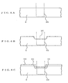
- Figs.4A, 4B and 4C are cross sectional views for explanation of each step in a first embodiment.
- Fig.5 is an expanded view of a bending portion.
- Figs.6A, 6B and 6C are cross sectional views for explanation of each step in a second embodiment.
- Figs.7A, 7B, 7C and 7D are cross sectional views for explanation of each step in a third embodiment.
- Fig.8 is a diagram illustrating a dicing at a dicing area where grooves are formed.
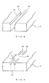
- Fig.9 is a diagram illustrating a structure of grooves formed at a dicing area.
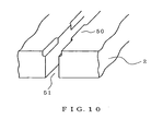
- Fig.10 is a diagram illustrating a dicing where the part between two parallel grooves shown in Fig.9 is cut.
- Fig.11 is a partial plan view of a wafer having one groove non-formed portion per dicing area.
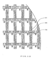
- Fig.12 is a partial plan view of a wafer having grooves non-formed portions provided for edges of all the chips.
- Figs.4A, 4B and 4C are cross sectional views for illustrating each step of a first embodiment.
- the fabrication process of semiconductor elements includes etching processes. Utilizing an etching process, for a dicing area 20 in a semiconductor substrate 2 of GaAs having 300 ⁇ m thickness as shown in Fig.4A, two parallel grooves 22 and 24 each having 10 ⁇ m width and 0.7 ⁇ m depth are formed by an etching process as shown in Fig.4B.
- "w" denotes the width and "t” the depth of each groove.
- the distance between the centers of grooves 22 and 24 is the same as the thickness of a dicing blade (not shown), 25 ⁇ m for example.
- an SiO 2 film 26 of 0.4 ⁇ m thickness is deposited on the inner surface of the grooves 22, 24 and the surface of the semiconductor substrate 2 as a surface protective film.
- a bending portion (or a crack caused portion) 28 is formed at the interface between the inner surface of the groove and the surface of the substrate.
- material for the surface protective film SiN, Al 2 O 3 , TiO 2 , Ta 2 O 5 and the like may be used other than SiO 2 .
- Fig.5 shows the bending portion 28 in expanded manner.
- the bending radius of the portion 28 is denoted by "R” and the bending angle " ⁇ ".
- the thickness of the protective film 26 is two times or more the radius R of the bending portion 28, and ⁇ is about 90°.
- the part between the two grooves 23 and 24 is diced to form a cut line.
- the both-side edges of the dicing blade pass through the bottoms of the two grooves, respectively.
- a stress caused in the protective film 26 by the edges of the blade during a dicing step is concentrated to the bending portion 28, causing a crack along the bending portion.
- the protective film 26 is disrupted at the bending portion, so that the stress caused by the edges of a dicing blade is not propagated to the area of semiconductor elements. Therefore, the peeling-off of the protective film is not caused at the area of the semiconductor elements.
- Figs.6A, 6B and 6C are cross sectional views for illustrating each step of a second embodiment.
- a dicing area 20 in a semiconductor substrate 2 of GaAs having 300 ⁇ m thickness as shown in Fig.6A one groove 30 having the width larger than the width (25 ⁇ m) of the dicing area is formed by an etching process as shown in Fig.6B.
- the groove 30 has 35 ⁇ m width and 0.7 ⁇ m depth.
- an SiO 2 film 26 of 0.4 ⁇ m thickness is deposited on the inner surface of the groove 30 and the surface of the semiconductor substrate 2 as a surface protective film.
- the central part of the groove 30 is diced to form a cut line.
- the both-side edges of the dicing blade pass through the bottom of one groove 30.
- a stress caused in the protective film 26 by the edges of the blade during a dicing step is concentrated to the bending portion 31 at the interface between the inner surface of the groove and the surface of the substrate, causing a crack along the bending portion.
- the protective film 26 is disrupted at the bending portion, so that the stress caused by the edges of a dicing blade is not propagated to the area of semiconductor elements. Therefore, the peeling-off of the protective film is not caused at the area of the semiconductor elements.
- Figs.7A, 7B and 7C are cross sectional views for illustrating each step of a third embodiment.
- a dicing area 20 in a semiconductor substrate 2 of GaAs having 300 ⁇ m thickness as shown in Fig.7A two parallel first grooves 22 and 24 each having 10 ⁇ m width and 0.7 ⁇ m depth are formed as shown in Fig.7B by an etching process in the same way as the first embodiment.
- Additional second grooves each having 5 ⁇ m width and 1.3 ⁇ m depth are formed in the bottom of the first grooves 22 and 24, respectively, by an etching process in such a manner that the second groove is parallel to the first groove in which the second one is provided. Therefore, the configuration of each groove consisted of the first and second ones has two-step shape. The distance between the centers of two grooves each having two-step shape is 25 ⁇ m as in the first embodiment.
- an SiO 2 film 26 having 0.4 ⁇ m thickness is deposited on the inner surface of the grooves and the surface of the substrate as a surface protective film.
- the part between the two grooves is diced to form a cut line.
- the both-side edges of the dicing blade pass through the bottoms of the two grooves, respectively.
- the peeling-off of the protective film 26 is substantially prevented at the bending portion 36 between the first groove and the second groove. If the peeling-off of the protective film in part proceeds over the bending portion 36, the peeling-off will be completely stopped at the bending portion 38 between the inner surface of the first groove and the surface of the substrate and then will not be caused at the area of the semiconductor element.
- each groove formed around a chip generally do not exceed the depth of the semiconductor element. This is because the grooves are formed by utilizing the etching step in the fabrication of semiconductor elements.
- the present invention is useful for grooves each having a depth larger than that of the element area, these grooves being formed by a etching process other than the etching process during the fabrication step of the elements.
- a full automatic dicing apparatus is generally used for dicing a semiconductor wafer into chips.
- the alignment of a wafer is carried out at first. This is automatically conducted by utilizing unique patterns on the wafer. Then, a dicing blade is moved to the position where a first dicing line seems to be in order to cut only one line. Then, a CCD camera is moved to the position where the cut line seems to be formed in order to search the cut line.
- the image of the cut line picked up by the CCD camera is darker than that of a peripheral part of the substrate, so that the cut line is recognized as "black” by processing the CCD image into binary.
- Fig.8 shows the substrate 2 after cutting, the substrate provided with grooves such as described in the first, second and third embodiments.
- the edge 40 of the groove and the edge 42 of the cut line 43 are parallel each other.
- the present embodiment is applicable to a semiconductor not having a protective film thereon, then a dicing step will be explained hereinafter for a wafer not provided with a protective film.
- a display for example CRT
- the full automatic dicing apparatus erroneously recognizes the groove edges as the cut line edges.
- an erroneous feedback is conducted in a next dicing, resulting in a displacement of a dicing position. Such displacements are accumulated until a cut line is correctly recognized, then the dicing position will have a large misregistration with respect to the target position.
- a part at which grooves are not formed i.e. a groove non-formed part is left without forming grooves across the overall length according to the present embodiment.
- Fig.9 shows the structure of such grooves including non-formed part, the grooves being provided in a dicing area 44 in a semiconductor wafer 2 of 300 ⁇ m thickness which is diced by a blade of 25 ⁇ m thickness.
- Two grooves 46 and 48 each having 5 ⁇ m width and 2 ⁇ m depth are formed in parallel by an etching process. The distance between the centers of two grooves is 25 ⁇ m, and the distance between the outer edges of two grooves is 30 ⁇ m.
- a groove non-formed part 50 having the length "L" of 50 ⁇ m is left near a chip alignment mark or a unique pattern (not shown).
- Fig.10 shows the substrate 2 after cutting the part between two grooves 46 and 48 in the substrate shown in Fig.9, the cut line being designated by reference numeral 51.
- the cut line 51 is picked by a CCD camera and is monitored by a display (CRT) having a magnification of 400, the length "L" of the groove non-formed part 50 is 20mm on the display. This shows that the length "L” is long enough to check the shape of the cut line 51 on the display.
- the width of "black” region is 12 mm, thereby it is recognized that the real width of "black” region on the wafer is 30 ⁇ m.
- This dimension i.e. 30 ⁇ m is recognized to be matched with the distance between the outer edges of the grooves 20 and 22. This dimension is also unchanged even if a dicing position is moved across 2.5 ⁇ m to the direction perpendicular to the longitudinal direction of grooves. This means that it is impossible to detect the edge of the cut line 51 accurately at the groove formed region.
- the width of the cut line 51 is recognized to be 10mm on the display and 25 ⁇ m in real dimension at the groove non-formed part 50.
- Fig.11 shows a wafer 62 in which grooves of the present invention are formed around chips 60 to be diced.
- Two parallel grooves 62 and 64 formed at the peripheral area of the wafer 62 is provided with only one groove non-formed part 66.
- Two parallel grooves 72 and 74 formed at the inward area of the wafer 62 is also provided with only one groove non-formed part 76.
- the positions of all the dicing areas are estimated by searching unique patterns 80 on chips. Based on this estimation, a dicing blade is moved to a dicing area where the grooves 62 and 64 are formed to cut only one line. Then, a CCD camera is moved to the position where a cut line is estimated to be in order to search the cut line. Furthermore, the position of a groove non-formed part 66 is estimated by the position of the unique pattern 80 and the groove non-formed part is picked up by a CCD camera. In the image picked up by the CCD camera, the cut line is necessarily darker than that of a peripheral part of the substrate.
- an estimated position of dicing area where the grooves 72 and 74 are formed is corrected and an area at the corrected position is then diced. And, the correct cut line edge is detected at the groove non-formed part 76 to correct a next dicing position.
- the same processing steps may be hereinafter repeated to dice a plurality of chips accurately from the wafer.
- the unique pattern 82 may be recognized as the unique pattern 80, so that the groove non-formed part 66 may be erroneously decided to be at the position 86.
- the groove non-formed parts 66 and 67 can be provided for all of chips, respectively, as shown in Fig.12. In this manner, a groove non-formed part may easily be searched from any unique pattern 80 which is neighbored thereto.
- a groove is formed at a dicing area to provide a surface protective film with a bending portion, so that the propagation of the peeling-off of the film toward an area of semiconductor elements is blocked.
- this method is conducted by utilizing etching steps during the fabrication of the elements, the step of etching away the film in the conventional method is not needed. As a result, the number of steps is not increased in the present invention.
- the groove non-formed part is provided for grooves to be formed at a dicing area, so that the position of a cut line may be accurately detected. As a result, a misregistration of a dicing position is not caused in a full automatic dicing apparatus.
Landscapes
- Dicing (AREA)
Abstract
A method for dicing a semiconductor wafer into chips is
provided, in which the peeling-off of a hard protective film
on the surface of a semiconductor substrate may be avoided.
Two parallel grooves are formed at a dicing area around a
chip by an etching process. Then, SiO2 film is deposited on
the GaAs substrate as a protective film. At this time, a
bending portion at the interface between the protective films
on the inner surface of the groove and the surface of the
substrate. When the part between two grooves is cut by a
dicing blade, a stress to the protective film caused by the
edge of the blade is concentrated to the bending portion,
resulting in a crack along the bending portion.
Description
- The present invention relates to a method for dicing a semiconductor wafer into chips, particularly to a method for dicing a semiconductor wafer provided with grooves in dicing areas. The present invention further relates to the structure of such grooves.
- When a semiconductor wafer (or a semiconductor substrate) on which semiconductor elements are built in is diced into chips, if the surface of the semiconductor wafer is covered by an electrically insulating hard protective film such as oxide film and nitride film, the peeling-off of the protective film is caused in the edge part of a cut line.
- With reference to Fig.1, the
protective film 4 provided on thesubstrate 2 is peeled off during a dicing step by ablade 6. Areference numeral 8 denotes a part of the film peeled off. - In order to prevent the peeling-off of the protective film conventionally, a dicing step is conducted after the protective film is etched away along a dicing line as shown in Fig. 2,
reference numeral 10 denoting the part of the protective film etched away. - According to the conventional dicing method in Fig. 2, the step for etching away the protective film is needed to be conducted other than the step for fabricating semiconductor elements, resulting in the problems of the increase of manufacturing steps and cost.
- When the semiconductor wafer is diced after the protective film is peeled off along dicing lines, the substrate is laid bare in the edge part of each diced chip. Accordingly, in the case where a
semiconductor element 12 is mounted on a printedcircuit board 14 and theelement 12 is connected to theboard 14 through alead wire 16 as shown in Fig.3, there is a possibility that thesubstrate 12 and thewire 16 are electrically shorted around theposition 18, resulting in the malfunction of thesemiconductor element 12. - An object of the present invention is to provide a method for dicing a semiconductor wafer which is covered by an electrically insulating hard protective film such as oxide film or nitride film to protect the surface of the wafer.
- Another object of the present invention is to provide a structure of grooves formed in dicing areas of the wafer.
- Still another object of the present invention is to provide a structure of grooves for preventing the displacement of the dicing position from being caused during a dicing step by an full automatic dicing apparatus.
- A further object of the present invention is to provide a method for detecting the edge of each cut line accurately.
- According to the present invention, grooves are formed in dicing area around each chip by utilizing etching steps during the fabrication of semiconductor elements. Then, a hard protective film is deposited on the inner surface the groove and the surface of the substrate. An edge of a dicing blade is aligned in such a manner that the edge passes through the bottom of the groove. A stress is applied upward or downward to the portion of the protective film to which the edge of the dicing blade is contacted. This stress is propagated from the protective film on the groove to the protective film on the substrate. At this time, the stress is concentrated to the bending portion at the interface between the protective films on the inner surface of the groove and the surface of the substrate, so that the crack is caused along the bending portion. The bending portion where such stress is caused is herein referred to as a crack caused portion.
- In order to cause such crack, it is required that the radius of the bending portion is substantially smaller than the thickness of the protective film. For example, if the radius of the bending portion is one-half the thickness of the protective film, a bending stress caused at the bending portion having a bending angle of 0 ° - 120 ° is 1.5 times that caused at another part of the film. Also, if the radius of the bending portion is one-tenth the thickness of the protective film, the pending stress caused at the pending portion is increased by 2.5 times that of a peripheral part of the film. If the radius of the bending portion is one-twentieth the thickness of the protective film, the bending stress is increased by 3.4 times that of a peripheral part of the film. While an acute angle is preferable for a bending angle of the bending portion, the angle of 90 ° is comparable to an acute angle.
- As a protective film is disrupted by a crack caused at the bending portion, the stress caused by the edge of the blade is not propagated to the area of a semiconductor element. Therefore, the peeling-off of the protective film is not caused at the area of a semiconductor element.
- The width of a groove is preferably about 1-20 µm. While a groove is preferably formed at both-side edges of a dicing line, respectively, a groove may be formed only at one-side edge of a dicing line in the case where only the area neighboring said one-side edge is required to be protected by the film. Alternatively, only one groove which has a width larger than the that of a dicing line may be formed in place of providing groove in both-side edges of a dicing line, respectively.
- When one or more etching steps are conducted in the fabricating process of semiconductor elements, an additional groove may be formed in the bottom of an already provided groove to increase the number of crack caused portions. In this case, if a stress has been propagated through a first crack caused portion, the propagation of the stress may be blocked at a second crack caused portion. As a result, the peeling-off of the protective film at the area of a semiconductor element may necessarily be avoided.
- Furthermore, according to the present invention, a groove non-formed part may be provided for grooves to be formed at a dicing area. An accurate position of the edge of a cut line may be detected at the groove non-formed part by means of a CCD camera. In this manner, the position of the edge of the cut line may be accurately recognized, so that a next dicing position estimated based on the accurate position of the edge of the cut line may also precisely recognized, i.e. an erroneous recognition for a dicing position is not caused. AS a result, a misregistration of a dicing position may be avoided.
- In the present invention, a groove non-formed part is needed to be provided at one or more positions for one dicing line which is required to have a more accurate dicing position. In most cases, as a plurality of chips each having the same configuration are arranged repeatedly on a wafer, it is easy to provide only one groove non-formed part at the peripheral part of each chip. As a result, a groove non-formed part may be easily searched by a CCD camera after dicing.
- Where the length of a groove non-formed part is too long, a chipping or a peeling-off of a protective film is caused, and where is too short, it becomes difficult to detect a accurate position of a cut line. When monitoring a groove non-formed part on a CRT with a magnification of 400, the length of a groove non-formed part is preferably about 10-100 µm.
- Also, a dicing method of the present invention comprising the steps of : a) detecting an edge of a cut line after cutting a first dicing area of the semiconductor wafer by picking up an image of an area of the cut line including the groove non-formed part by an image pick-up device ; b) correcting a next dicing position stored in the full automatic dicing apparatus based on the edge of the cut line detected ; c) cutting a next dicing area based on the next dicing position corrected ; d) detecting an edge of a cut line after cutting the next dicing area in the step c) by picking up an image of an area of the cut line including the groove non-formed part by an image pick-up device ; e) correcting a further next dicing position stored in the full automatic dicing apparatus based on the edge of the cut line detected in the step d) ; f) cutting a further next dicing area based on the further next dicing position corrected in the step e) ; and g) repeating the steps d) - f).
- It should be noted that the dicing method of the present invention is applicable to not only a semiconductor wafer provided with a protective film thereon but also a semiconductor wafer not provided with a protective film thereon.
- Fig.1 is a diagram illustrating the peeling-off of a surface protective film during a dicing step.
- Fig.2 is a diagram illustrating an example of a conventional dicing method.
- Fig.3 is a diagram illustrating an electrical short between a semiconductor substrate and a lead wire.
- Figs.4A, 4B and 4C are cross sectional views for explanation of each step in a first embodiment.
- Fig.5 is an expanded view of a bending portion.
- Figs.6A, 6B and 6C are cross sectional views for explanation of each step in a second embodiment.
- Figs.7A, 7B, 7C and 7D are cross sectional views for explanation of each step in a third embodiment.
- Fig.8 is a diagram illustrating a dicing at a dicing area where grooves are formed.
- Fig.9 is a diagram illustrating a structure of grooves formed at a dicing area.
- Fig.10 is a diagram illustrating a dicing where the part between two parallel grooves shown in Fig.9 is cut.
- Fig.11 is a partial plan view of a wafer having one groove non-formed portion per dicing area.
- Fig.12 is a partial plan view of a wafer having grooves non-formed portions provided for edges of all the chips.
- Embodiments of the present invention will now be described in detail with reference to the drawings.
- Figs.4A, 4B and 4C are cross sectional views for illustrating each step of a first embodiment. In general, the fabrication process of semiconductor elements includes etching processes. Utilizing an etching process, for a
dicing area 20 in asemiconductor substrate 2 of GaAs having 300µm thickness as shown in Fig.4A, twoparallel grooves grooves - Then, as shown in Fig.4C, an SiO2 film 26 of 0.4µm thickness is deposited on the inner surface of the
grooves semiconductor substrate 2 as a surface protective film. At this time, a bending portion (or a crack caused portion) 28 is formed at the interface between the inner surface of the groove and the surface of the substrate. As material for the surface protective film, SiN, Al2O3, TiO2, Ta2O5 and the like may be used other than SiO2. - Fig.5 shows the bending
portion 28 in expanded manner. The bending radius of theportion 28 is denoted by "R" and the bending angle "". In this embodiment, the thickness of theprotective film 26 is two times or more the radius R of the bendingportion 28, and is about 90°. - Using a dicing blade (not shown) of 25µm thickness, the part between the two
grooves 23 and 24 is diced to form a cut line. During a dicing step, the both-side edges of the dicing blade pass through the bottoms of the two grooves, respectively. At this time, a stress caused in theprotective film 26 by the edges of the blade during a dicing step is concentrated to the bendingportion 28, causing a crack along the bending portion. Theprotective film 26 is disrupted at the bending portion, so that the stress caused by the edges of a dicing blade is not propagated to the area of semiconductor elements. Therefore, the peeling-off of the protective film is not caused at the area of the semiconductor elements. - Figs.6A, 6B and 6C are cross sectional views for illustrating each step of a second embodiment. For a
dicing area 20 in asemiconductor substrate 2 of GaAs having 300µm thickness as shown in Fig.6A, onegroove 30 having the width larger than the width (25µm) of the dicing area is formed by an etching process as shown in Fig.6B. Thegroove 30 has 35 µm width and 0.7µm depth. Then, as shown in Fig.6C, an SiO2 film 26 of 0.4µm thickness is deposited on the inner surface of thegroove 30 and the surface of thesemiconductor substrate 2 as a surface protective film. - Using a dicing blade (not shown) of 25µm thickness, the central part of the
groove 30 is diced to form a cut line. During a dicing step, the both-side edges of the dicing blade pass through the bottom of onegroove 30. At this time, a stress caused in theprotective film 26 by the edges of the blade during a dicing step is concentrated to the bendingportion 31 at the interface between the inner surface of the groove and the surface of the substrate, causing a crack along the bending portion. Theprotective film 26 is disrupted at the bending portion, so that the stress caused by the edges of a dicing blade is not propagated to the area of semiconductor elements. Therefore, the peeling-off of the protective film is not caused at the area of the semiconductor elements. - Figs.7A, 7B and 7C are cross sectional views for illustrating each step of a third embodiment. According to this embodiment, for a
dicing area 20 in asemiconductor substrate 2 of GaAs having 300 µm thickness as shown in Fig.7A, two parallelfirst grooves - Additional second grooves each having 5µm width and 1.3 µm depth are formed in the bottom of the
first grooves - Then, as shown in Fig.7D, an SiO2 film 26 having 0.4µm thickness is deposited on the inner surface of the grooves and the surface of the substrate as a surface protective film.
- Using a dicing blade of 25 µm thickness, the part between the two grooves is diced to form a cut line. During a dicing step, the both-side edges of the dicing blade pass through the bottoms of the two grooves, respectively. In this case, the peeling-off of the
protective film 26 is substantially prevented at the bendingportion 36 between the first groove and the second groove. If the peeling-off of the protective film in part proceeds over the bendingportion 36, the peeling-off will be completely stopped at the bendingportion 38 between the inner surface of the first groove and the surface of the substrate and then will not be caused at the area of the semiconductor element. - In this manner, the propagation of the peeling-off of the protective film to the element area may be completely prevented by providing a plurality of crack caused portions. It is understood for those who skilled in the art that the method in this embodiment may be applicable to the second embodiment.
- While three embodiment have described heretofore, the depth of each groove formed around a chip generally do not exceed the depth of the semiconductor element. This is because the grooves are formed by utilizing the etching step in the fabrication of semiconductor elements. The present invention, however, is useful for grooves each having a depth larger than that of the element area, these grooves being formed by a etching process other than the etching process during the fabrication step of the elements.
- A full automatic dicing apparatus is generally used for dicing a semiconductor wafer into chips. According to the full automatic dicing apparatus, the alignment of a wafer is carried out at first. This is automatically conducted by utilizing unique patterns on the wafer. Then, a dicing blade is moved to the position where a first dicing line seems to be in order to cut only one line. Then, a CCD camera is moved to the position where the cut line seems to be formed in order to search the cut line. The image of the cut line picked up by the CCD camera is darker than that of a peripheral part of the substrate, so that the cut line is recognized as "black" by processing the CCD image into binary.
- Fig.8 shows the
substrate 2 after cutting, the substrate provided with grooves such as described in the first, second and third embodiments. In the figure, theedge 40 of the groove and theedge 42 of thecut line 43 are parallel each other. - It should be noted that the present embodiment is applicable to a semiconductor not having a protective film thereon, then a dicing step will be explained hereinafter for a wafer not provided with a protective film.
- Returning to Fig.8, monitoring these edges by a display (for example CRT) connected to the CCD camera, it is impossible to distinguish the
edge 42 of thecut line 43 formed by a dicing step from theedge 40 of the groove formed by an etching step. That is, theedge 40 of the groove looks as "black" as theedge 42 of the cut line on the display. Therefore, the full automatic dicing apparatus erroneously recognizes the groove edges as the cut line edges. In such a case, an erroneous feedback is conducted in a next dicing, resulting in a displacement of a dicing position. Such displacements are accumulated until a cut line is correctly recognized, then the dicing position will have a large misregistration with respect to the target position. - In order to prevent such misregistration of the dicing position, a part at which grooves are not formed, i.e. a groove non-formed part is left without forming grooves across the overall length according to the present embodiment.
- Fig.9 shows the structure of such grooves including non-formed part, the grooves being provided in a
dicing area 44 in asemiconductor wafer 2 of 300 µm thickness which is diced by a blade of 25 µm thickness. Twogrooves non-formed part 50 having the length "L" of 50 µm is left near a chip alignment mark or a unique pattern (not shown). - Fig.10 shows the
substrate 2 after cutting the part between twogrooves reference numeral 51. When thecut line 51 is picked by a CCD camera and is monitored by a display (CRT) having a magnification of 400, the length "L" of the groovenon-formed part 50 is 20mm on the display. This shows that the length "L" is long enough to check the shape of thecut line 51 on the display. - Monitoring a groove formed area of the
wafer 2 on the display, the width of "black" region is 12 mm, thereby it is recognized that the real width of "black" region on the wafer is 30 µm. This dimension (i.e. 30 µm) is recognized to be matched with the distance between the outer edges of thegrooves cut line 51 accurately at the groove formed region. - In contrast to this, the width of the
cut line 51 is recognized to be 10mm on the display and 25 µm in real dimension at the groovenon-formed part 50. This shows that the both-side edges of the cut line are inwardly apart by 2.5 µm from the outer edges of thegrooves - Fig.11 shows a
wafer 62 in which grooves of the present invention are formed aroundchips 60 to be diced. Twoparallel grooves wafer 62 is provided with only one groovenon-formed part 66. Twoparallel grooves wafer 62 is also provided with only one groovenon-formed part 76. - In a full automatic dicing apparatus, the positions of all the dicing areas are estimated by searching
unique patterns 80 on chips. Based on this estimation, a dicing blade is moved to a dicing area where thegrooves non-formed part 66 is estimated by the position of theunique pattern 80 and the groove non-formed part is picked up by a CCD camera. In the image picked up by the CCD camera, the cut line is necessarily darker than that of a peripheral part of the substrate. By processing the CCD image into binary, it is possible to recognize the portion of "black" as a cut line and the interface portion between "black" and "white" as the edge of the cut line. As shown in Fig.10, the edge in the groovenon-formed part 50 monitored by the CCD camera designates a correct cut line edge. Therefore, a correct cut line edge may be detected at the area of the groovenon-formed part 66 in Fig.11. - Based on the position of the cut line edge thus obtained, an estimated position of dicing area where the
grooves non-formed part 76 to correct a next dicing position. The same processing steps may be hereinafter repeated to dice a plurality of chips accurately from the wafer. - In the case where only one groove non-formed part is provided for each dicing area, if the position of a wafer mounted to the full automatic dicing apparatus is deviated from the correct position, the
unique pattern 82 may be recognized as theunique pattern 80, so that the groovenon-formed part 66 may be erroneously decided to be at theposition 86. In order to prevent such error, the groovenon-formed parts unique pattern 80 which is neighbored thereto. - According to the present invention described above, a groove is formed at a dicing area to provide a surface protective film with a bending portion, so that the propagation of the peeling-off of the film toward an area of semiconductor elements is blocked. As this method is conducted by utilizing etching steps during the fabrication of the elements, the step of etching away the film in the conventional method is not needed. As a result, the number of steps is not increased in the present invention.
- Furthermore, according to the present invention, the groove non-formed part is provided for grooves to be formed at a dicing area, so that the position of a cut line may be accurately detected. As a result, a misregistration of a dicing position is not caused in a full automatic dicing apparatus.
Claims (15)
- A method for dicing a semiconductor wafer into chips, comprising the steps of :forming at least one groove at a dicing area of a semiconductor substrate utilizing etching steps for the semiconductor substrate during the fabrication of semiconductor elements ;depositing a hard protective film on the inner surface of the at least one groove and the surface of the substrate ; andcutting the substrate by a dicing blade in such a manner that the edge of the dicing blade passes through the bottom of the at least one groove ; andwherein a crack is caused at a bending portion at the interface between the protective films on the inner surface of the at least groove and the surface of the substrate during the cutting step.
- The method of claim 1, wherein two parallel grooves are formed, and the both-side edges of the dicing blade pass through the bottoms of the two grooves, respectively.
- The method of claim 1, wherein one groove is formed, and the one-side edge of the dicing blade pass through the bottom of the one groove.
- The method of claim 1, wherein one groove is formed, and the both-side edges of the dicing blade pass through the bottom of the one groove.
- A method for dicing a semiconductor wafer into chips, comprising the steps of :forming at least one first groove at a dicing area of a semiconductor substrate utilizing etching steps for the semiconductor substrate during the fabrication of semiconductor elements ;forming one second groove at the bottom of the at least one first groove in parallel therewith utilizing etching steps for the semiconductor substrate during the fabrication of semiconductor elements ;depositing a hard protective film on the inner surfaces of the first and second grooves and the surface of the substrate ; andcutting the substrate in such a manner that the edge of a dicing blade passes through the bottom of the second groove ; andwherein a crack is caused at a bending portion at the interface between the protective films at the interface between the protective films on the inner surfaces of the first and second grooves, or at the interface between the protective films on the inner surface of the first groove and the surface of the substrate during the cutting step.
- The method of any one of claims 1-5, wherein the protective film is an electrical insulating material.
- The method of any one of claims 1-5, wherein the protective film is SiO2, SiN, Al2O3, TiO2, or Ta2O5.
- A structure of grooves formed at a dicing area for dicing a semiconductor wafer into chips, comprising :
two parallel grooves including at least one groove non-formed part. - The structure of claim 8, wherein the two parallel grooves are formed by an etching process.
- The structure of claim 9, wherein the length of the groove non-formed part in a longitudinal direction of the two grooves is 10-100µm.
- A semiconductor wafer comprising a structure of grooves of any one of claims 8-10.
- The semiconductor wafer of claim 11, wherein the groove non-formed part is provided at least one position around each chip.
- A method for detecting an edge of a cut line, comprising the steps of :cutting a semiconductor wafer of claim 11 to form a cut line by a dicing blade in such a manner that the both-side edges of the dicing blade pass through the bottoms of the two grooves, respectively ;picking up an image of an area of the cut line including the groove non-formed part by an image pick-up device ; anddetecting an edge of the cut line from the image picked up by the image pick-up device.
- The method of claim 13, wherein the image pick-up device is a CCD camera.
- A method for dicing a semiconductor wafer of claim 11 into chips by a full automatic dicing apparatus, comprising the steps of :a) detecting an edge of a cut line after cutting a first dicing area of the semiconductor wafer by picking up an image of an area of the cut line including the groove non-formed part by an image pick-up device ;b) correcting a next dicing position stored in the full automatic dicing apparatus based on the edge of the cut line detected ;c) cutting a next dicing area based on the next dicing position corrected ;d) detecting an edge of a cut line after cutting the next dicing area in the step c) by picking up an image of an area of the cut line including the groove non-formed part by an image pick-up device ;e) correcting a further next dicing position stored in the full automatic dicing apparatus based on the edge of the cut line detected in the step d) ;f) cutting a further next dicing area based on the further next dicing position corrected in the step e) ; andg) repeating the steps d) - f).
Applications Claiming Priority (5)
| Application Number | Priority Date | Filing Date | Title |
|---|---|---|---|
| JP21667999 | 1999-07-30 | ||
| JP21667999A JP4581158B2 (en) | 1999-07-30 | 1999-07-30 | Semiconductor substrate cutting method |
| JP22827999A JP2001053032A (en) | 1999-08-12 | 1999-08-12 | Structure of dicing groove provided in semiconductor dicing area and dicing method |
| JP22827999 | 1999-08-12 | ||
| PCT/JP2000/004939 WO2001009932A1 (en) | 1999-07-30 | 2000-07-25 | Method of dicing semiconductor wafer into chips, and structure of groove formed in dicing area |
Publications (1)
| Publication Number | Publication Date |
|---|---|
| EP1130629A1 true EP1130629A1 (en) | 2001-09-05 |
Family
ID=26521570
Family Applications (1)
| Application Number | Title | Priority Date | Filing Date |
|---|---|---|---|
| EP00946479A Withdrawn EP1130629A1 (en) | 1999-07-30 | 2000-07-25 | Method of dicing semiconductor wafer into chips, and structure of groove formed in dicing area |
Country Status (7)
| Country | Link |
|---|---|
| US (1) | US6300224B1 (en) |
| EP (1) | EP1130629A1 (en) |
| KR (1) | KR100660310B1 (en) |
| CN (1) | CN1322574C (en) |
| CA (1) | CA2345739A1 (en) |
| TW (1) | TW476142B (en) |
| WO (1) | WO2001009932A1 (en) |
Cited By (1)
| Publication number | Priority date | Publication date | Assignee | Title |
|---|---|---|---|---|
| US6573156B1 (en) | 2001-12-13 | 2003-06-03 | Omm, Inc. | Low defect method for die singulation and for structural support for handling thin film devices |
Families Citing this family (51)
| Publication number | Priority date | Publication date | Assignee | Title |
|---|---|---|---|---|
| JP2001320007A (en) * | 2000-05-09 | 2001-11-16 | Dainippon Printing Co Ltd | Frame for resin-encapsulated semiconductor device |
| JP4349541B2 (en) | 2000-05-09 | 2009-10-21 | 大日本印刷株式会社 | Resin-encapsulated semiconductor device frame |
| JP4840893B2 (en) | 2000-05-12 | 2011-12-21 | 大日本印刷株式会社 | Resin-encapsulated semiconductor device frame |
| KR100386817B1 (en) * | 2001-06-28 | 2003-06-09 | 동부전자 주식회사 | Method for fabricating a chip scale type semiconductor package |
| TWI226139B (en) | 2002-01-31 | 2005-01-01 | Osram Opto Semiconductors Gmbh | Method to manufacture a semiconductor-component |
| TWI232560B (en) * | 2002-04-23 | 2005-05-11 | Sanyo Electric Co | Semiconductor device and its manufacture |
| TWI229435B (en) * | 2002-06-18 | 2005-03-11 | Sanyo Electric Co | Manufacture of semiconductor device |
| TWI272641B (en) * | 2002-07-16 | 2007-02-01 | Semiconductor Energy Lab | Method of manufacturing a semiconductor device |
| TWI227550B (en) * | 2002-10-30 | 2005-02-01 | Sanyo Electric Co | Semiconductor device manufacturing method |
| JP4904150B2 (en) * | 2003-01-31 | 2012-03-28 | オスラム オプト セミコンダクターズ ゲゼルシャフト ミット ベシュレンクテル ハフツング | Method for manufacturing light emitting device |
| EP2894678A1 (en) * | 2003-01-31 | 2015-07-15 | Osram Opto Semiconductors Gmbh | Method for making a semiconductor component |
| TW200418149A (en) * | 2003-03-11 | 2004-09-16 | Siliconware Precision Industries Co Ltd | Surface-mount-enhanced lead frame and method for fabricating semiconductor package with the same |
| WO2004097916A1 (en) * | 2003-04-30 | 2004-11-11 | Fujitsu Limited | Method for fabricating semiconductor device, semiconductor wafer and semiconductor device |
| JP4401181B2 (en) * | 2003-08-06 | 2010-01-20 | 三洋電機株式会社 | Semiconductor device and manufacturing method thereof |
| JP2005064230A (en) * | 2003-08-12 | 2005-03-10 | Disco Abrasive Syst Ltd | How to divide a plate |
| US7183137B2 (en) * | 2003-12-01 | 2007-02-27 | Taiwan Semiconductor Manufacturing Company | Method for dicing semiconductor wafers |
| JP2005195965A (en) * | 2004-01-08 | 2005-07-21 | Sharp Corp | Hologram element, manufacturing method thereof, and electro-optical component |
| EP1774587B1 (en) * | 2004-07-26 | 2009-10-07 | Nxp B.V. | Wafer with improved conductive loops in the dicing lines |
| JP4322181B2 (en) * | 2004-07-29 | 2009-08-26 | 三洋電機株式会社 | Manufacturing method of semiconductor device |
| US7518217B2 (en) * | 2004-11-11 | 2009-04-14 | Yamaha Corporation | Semiconductor device, semiconductor wafer, chip size package, and methods of manufacturing and inspection therefor |
| US20060125059A1 (en) * | 2004-12-15 | 2006-06-15 | Taiwan Semiconductor Manufacturing Co., Ltd. | Semiconductor wafer with protection structure against damage during a die separation process |
| JP4694845B2 (en) * | 2005-01-05 | 2011-06-08 | 株式会社ディスコ | Wafer division method |
| KR20070087104A (en) * | 2005-02-18 | 2007-08-27 | 미쓰이 가가쿠 가부시키가이샤 | Semiconductor wafer surface protection sheet and protection method of semiconductor wafer using the protection sheet |
| JP4751634B2 (en) | 2005-03-31 | 2011-08-17 | 富士通セミコンダクター株式会社 | Manufacturing method of semiconductor device |
| CN100407403C (en) * | 2005-06-28 | 2008-07-30 | 联华电子股份有限公司 | semiconductor wafer |
| EP1764834B1 (en) * | 2005-09-15 | 2009-03-04 | Infineon Technologies AG | Electromagnetic shielding of packages with a laminate substrate |
| WO2007055010A1 (en) | 2005-11-10 | 2007-05-18 | Renesas Technology Corp. | Semiconductor device manufacturing method and semiconductor device |
| TWI324800B (en) * | 2005-12-28 | 2010-05-11 | Sanyo Electric Co | Method for manufacturing semiconductor device |
| JP4990801B2 (en) * | 2006-01-31 | 2012-08-01 | エルジー ディスプレイ カンパニー リミテッド | EL device |
| JP4533392B2 (en) * | 2006-03-22 | 2010-09-01 | キヤノン株式会社 | Organic light emitting device |
| JP4898497B2 (en) * | 2006-03-27 | 2012-03-14 | キヤノン株式会社 | Organic light emitting device and method for manufacturing the same |
| CN100514602C (en) * | 2006-07-18 | 2009-07-15 | 中华映管股份有限公司 | Wafer cutting method |
| US7838424B2 (en) * | 2007-07-03 | 2010-11-23 | Taiwan Semiconductor Manufacturing Company, Ltd. | Enhanced reliability of wafer-level chip-scale packaging (WLCSP) die separation using dry etching |
| DE102011101035B4 (en) * | 2011-05-10 | 2014-07-10 | Infineon Technologies Ag | A method of manufacturing a terminal region on a sidewall of a semiconductor body |
| CN103493589B (en) | 2011-09-26 | 2016-05-18 | 松下电器产业株式会社 | The manufacture method of light-emitting device and light-emitting device |
| JP6184855B2 (en) * | 2013-12-16 | 2017-08-23 | 株式会社ディスコ | Package substrate division method |
| CN104973562A (en) * | 2014-04-03 | 2015-10-14 | 中芯国际集成电路制造(上海)有限公司 | Wafer cutting method and MEMS wafer cutting method |
| JP6430009B2 (en) * | 2015-07-07 | 2018-11-28 | 三菱電機株式会社 | Manufacturing method of semiconductor device |
| EP3144271B1 (en) * | 2015-09-21 | 2019-03-27 | Point Engineering Co., Ltd. | Unit anodic oxide film structure |
| CN106558539A (en) * | 2015-09-25 | 2017-04-05 | 上海先进半导体制造股份有限公司 | The scribing of chip and manufacture method |
| DE102015120756A1 (en) * | 2015-11-30 | 2017-06-01 | Infineon Technologies Ag | Method of separating a plurality of chips |
| KR101747856B1 (en) * | 2017-02-09 | 2017-06-15 | (주)포인트엔지니어링 | Cutting method for Anodic oxide film structure and Unit Anodic oxide film structure using the same |
| KR102255758B1 (en) | 2017-04-26 | 2021-05-26 | 삼성전자주식회사 | Semiconductor device package and method for fabricating the same |
| CN107188111A (en) * | 2017-05-27 | 2017-09-22 | 龙微科技无锡有限公司 | The splinter method of MEMS sensor wafer, MEMS sensor wafer |
| DE102017125276A1 (en) | 2017-10-27 | 2019-05-02 | Osram Opto Semiconductors Gmbh | Method for producing a plurality of semiconductor chips and semiconductor chip |
| DE102018214337B4 (en) * | 2018-08-24 | 2026-05-13 | Disco Corporation | Methods for processing a substrate |
| CN114530414A (en) * | 2019-03-29 | 2022-05-24 | 长江存储科技有限责任公司 | Method for manufacturing semiconductor chip |
| CN110091442B (en) * | 2019-05-15 | 2021-07-23 | 德淮半导体有限公司 | A kind of cutter for cutting wafer and cutting method |
| CN112885923A (en) * | 2020-08-12 | 2021-06-01 | 北京绿波静心新能源科技有限公司 | Silicon solar cell preparation method, silicon wafer and silicon solar cell |
| CN118763058A (en) * | 2024-08-19 | 2024-10-11 | 合肥领航微系统集成有限公司 | A structure, method and process for facilitating wafer dicing |
| CN119153412B (en) * | 2024-08-19 | 2026-01-23 | 合肥领航微系统集成有限公司 | Slotting structure, slotting method and scribing process for wafer scribing |
Family Cites Families (7)
| Publication number | Priority date | Publication date | Assignee | Title |
|---|---|---|---|---|
| DE2730130C2 (en) * | 1976-09-14 | 1987-11-12 | Mitsubishi Denki K.K., Tokyo | Method for manufacturing semiconductor components |
| JPS5776860A (en) * | 1980-10-31 | 1982-05-14 | Toshiba Corp | Semiconductor device and its manufacture |
| JPH04236447A (en) * | 1991-01-21 | 1992-08-25 | Nec Corp | Scribing line detection apparatus |
| JPH06112312A (en) * | 1992-09-24 | 1994-04-22 | Rohm Co Ltd | Semiconductor chip manufacturing method |
| JPH06232254A (en) | 1993-02-01 | 1994-08-19 | Sumitomo Electric Ind Ltd | Method and device for detecting cutting line position of semiconductor wafer |
| JPH06236447A (en) | 1993-02-09 | 1994-08-23 | Mitsubishi Electric Corp | Microcomputer for ic card |
| JPH06275713A (en) * | 1993-03-19 | 1994-09-30 | Hitachi Ltd | Semiconductor wafer, semiconductor chip, and dicing method |
-
2000
- 2000-07-25 EP EP00946479A patent/EP1130629A1/en not_active Withdrawn
- 2000-07-25 CA CA002345739A patent/CA2345739A1/en not_active Abandoned
- 2000-07-25 CN CNB008014981A patent/CN1322574C/en not_active Expired - Fee Related
- 2000-07-25 WO PCT/JP2000/004939 patent/WO2001009932A1/en not_active Ceased
- 2000-07-25 US US09/806,262 patent/US6300224B1/en not_active Expired - Lifetime
- 2000-07-25 KR KR1020017004026A patent/KR100660310B1/en not_active Expired - Lifetime
- 2000-07-28 TW TW089115107A patent/TW476142B/en not_active IP Right Cessation
Non-Patent Citations (1)
| Title |
|---|
| See references of WO0109932A1 * |
Cited By (1)
| Publication number | Priority date | Publication date | Assignee | Title |
|---|---|---|---|---|
| US6573156B1 (en) | 2001-12-13 | 2003-06-03 | Omm, Inc. | Low defect method for die singulation and for structural support for handling thin film devices |
Also Published As
| Publication number | Publication date |
|---|---|
| CA2345739A1 (en) | 2001-02-08 |
| CN1322574C (en) | 2007-06-20 |
| CN1318206A (en) | 2001-10-17 |
| TW476142B (en) | 2002-02-11 |
| WO2001009932A1 (en) | 2001-02-08 |
| KR20010075461A (en) | 2001-08-09 |
| KR100660310B1 (en) | 2006-12-22 |
| US6300224B1 (en) | 2001-10-09 |
Similar Documents
| Publication | Publication Date | Title |
|---|---|---|
| US6300224B1 (en) | Methods of dicing semiconductor wafer into chips, and structure of groove formed in dicing area | |
| KR100682003B1 (en) | Semiconductor device and manufacturing method thereof | |
| US6309943B1 (en) | Precision marking and singulation method | |
| US20040017013A1 (en) | Semiconductor device having a step-like section on the back side of the substrate, and method for manufacturing the same | |
| US20100007035A1 (en) | Semiconductor device and method of manufacturing the same | |
| KR20080055762A (en) | Semiconductor device and manufacturing method thereof | |
| US6441504B1 (en) | Precision aligned and marked structure | |
| US20020036357A1 (en) | Semiconductor device comprising layered positional detection marks and manufacturing method thereof | |
| JP4704792B2 (en) | GLASS SUBSTRATE WITH THIN FILM, ITS MANUFACTURING METHOD, AND SEMICONDUCTOR DEVICE USING THE SAME | |
| EP3576144B1 (en) | Semiconductor device | |
| KR19980018002A (en) | Semiconductor device and manufacturing method thereof | |
| US6974761B2 (en) | Method of forming a semiconductor laser chip having a marker | |
| CN114725067A (en) | Semiconductor device with a plurality of transistors | |
| US8264092B2 (en) | Integrated circuits on a wafer and method of producing integrated circuits | |
| JP4581158B2 (en) | Semiconductor substrate cutting method | |
| JP2004022631A (en) | Semiconductor device and pattern arrangement method | |
| US7022614B2 (en) | Method of etching back of semiconductor wafer | |
| KR101060699B1 (en) | Wafer alignment device and method | |
| JP3872031B2 (en) | Manufacturing method of semiconductor device | |
| US20240071971A1 (en) | Semiconductor device and manufacturing method of semiconductor device | |
| KR200302460Y1 (en) | semiconductor chip with pattern for recognition of chip bonding position for stacking semiconductor chip | |
| JPH1187219A (en) | Semiconductor device and manufacturing method thereof | |
| JP2663638B2 (en) | Method for manufacturing semiconductor device | |
| KR100242634B1 (en) | Pad structure of semiconductor device and manufacturing method thereof | |
| JP2001053032A (en) | Structure of dicing groove provided in semiconductor dicing area and dicing method |
Legal Events
| Date | Code | Title | Description |
|---|---|---|---|
| PUAI | Public reference made under article 153(3) epc to a published international application that has entered the european phase |
Free format text: ORIGINAL CODE: 0009012 |
|
| AK | Designated contracting states |
Kind code of ref document: A1 Designated state(s): AT BE CH CY DE DK ES FI FR GB GR IE IT LI LU MC NL PT SE |
|
| AX | Request for extension of the european patent |
Free format text: AL;LT;LV;MK;RO;SI |
|
| 17P | Request for examination filed |
Effective date: 20010911 |
|
| STAA | Information on the status of an ep patent application or granted ep patent |
Free format text: STATUS: THE APPLICATION HAS BEEN WITHDRAWN |
|
| 18W | Application withdrawn |
Effective date: 20040514 |