EP1127308B1 - Verfahren und gerät für leistungssteuerung in einem speicheruntersystem - Google Patents
Verfahren und gerät für leistungssteuerung in einem speicheruntersystem Download PDFInfo
- Publication number
- EP1127308B1 EP1127308B1 EP99971533A EP99971533A EP1127308B1 EP 1127308 B1 EP1127308 B1 EP 1127308B1 EP 99971533 A EP99971533 A EP 99971533A EP 99971533 A EP99971533 A EP 99971533A EP 1127308 B1 EP1127308 B1 EP 1127308B1
- Authority
- EP
- European Patent Office
- Prior art keywords
- group
- row
- memory
- rows
- pool
- Prior art date
- Legal status (The legal status is an assumption and is not a legal conclusion. Google has not performed a legal analysis and makes no representation as to the accuracy of the status listed.)
- Expired - Lifetime
Links
Images


Classifications
-
- G—PHYSICS
- G06—COMPUTING; CALCULATING OR COUNTING
- G06F—ELECTRIC DIGITAL DATA PROCESSING
- G06F1/00—Details not covered by groups G06F3/00 - G06F13/00 and G06F21/00
- G06F1/26—Power supply means, e.g. regulation thereof
- G06F1/32—Means for saving power
- G06F1/3203—Power management, i.e. event-based initiation of a power-saving mode
- G06F1/3206—Monitoring of events, devices or parameters that trigger a change in power modality
- G06F1/3215—Monitoring of peripheral devices
- G06F1/3225—Monitoring of peripheral devices of memory devices
-
- G—PHYSICS
- G06—COMPUTING; CALCULATING OR COUNTING
- G06F—ELECTRIC DIGITAL DATA PROCESSING
- G06F1/00—Details not covered by groups G06F3/00 - G06F13/00 and G06F21/00
- G06F1/26—Power supply means, e.g. regulation thereof
- G06F1/32—Means for saving power
- G06F1/3203—Power management, i.e. event-based initiation of a power-saving mode
- G06F1/3234—Power saving characterised by the action undertaken
- G06F1/325—Power saving in peripheral device
- G06F1/3275—Power saving in memory, e.g. RAM, cache
-
- G—PHYSICS
- G06—COMPUTING; CALCULATING OR COUNTING
- G06F—ELECTRIC DIGITAL DATA PROCESSING
- G06F12/00—Accessing, addressing or allocating within memory systems or architectures
- G06F12/02—Addressing or allocation; Relocation
- G06F12/06—Addressing a physical block of locations, e.g. base addressing, module addressing, memory dedication
-
- Y—GENERAL TAGGING OF NEW TECHNOLOGICAL DEVELOPMENTS; GENERAL TAGGING OF CROSS-SECTIONAL TECHNOLOGIES SPANNING OVER SEVERAL SECTIONS OF THE IPC; TECHNICAL SUBJECTS COVERED BY FORMER USPC CROSS-REFERENCE ART COLLECTIONS [XRACs] AND DIGESTS
- Y02—TECHNOLOGIES OR APPLICATIONS FOR MITIGATION OR ADAPTATION AGAINST CLIMATE CHANGE
- Y02D—CLIMATE CHANGE MITIGATION TECHNOLOGIES IN INFORMATION AND COMMUNICATION TECHNOLOGIES [ICT], I.E. INFORMATION AND COMMUNICATION TECHNOLOGIES AIMING AT THE REDUCTION OF THEIR OWN ENERGY USE
- Y02D10/00—Energy efficient computing, e.g. low power processors, power management or thermal management
Definitions
- the present invention relates to system memory power management in a computer system; more particularly, the present invention relates to power management in memory subsystems.
- SDRAMs Synchronous Dynamic Random Access Memories
- typical SDRAMs operate at speeds up to 66Mhz.
- the power generated by SDRAMs operating at such speeds is relatively low.
- RDRAMs Rambus Dynamic Random Access Memories
- SDRAMs are capable of operating at speeds up to 100Mhz, while RDRAMs operate at clock speeds up to 400Mhz and transfer rate up to 800 MHz.
- Memory devices operating at such high speed result in a significant amount of power being generated within the device (e.g., on the order of 2.1 watts for RDRAMs). The generation of this magnitude of power may potentially create thermal issues at the memory device.
- WO 00/26752 which has an earlier priority date than the present application but a publication date which is after the priority date of the present application, discloses a computer system employing DRAM devices which are assigned into particular pools corresponding to different power consumption states with a most recently accessed device being assigned to an active pool and placed at the top of a stack structure.
- a least recently accessed device in the active pool is evicted from the pool and placed in a standby pool when the active pool is full and the processor accesses another device which is not currently assigned to the active pool.
- a least recently active device of the standby pool is evicted into a nap pool when either a time-out occurs or the standby and active pools are full and the processors accesses another device which is not currently assigned to either the active or standby pools.
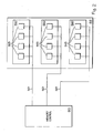
- FIG. 1 is a block diagram of one embodiment of a computer system 500.
- Computer system 500 includes a bus 501, a memory controller 510, a memory unit 515 and CPU 105. As described above, CPU 105 processes information received from memory 515 or other internal and external devices of computer system 500.
- Memory controller 510 is coupled to CPU 105. Memory controller 510 interfaces with memory unit 515 in order to carry out memory transactions.
- Memory unit 515 is coupled to memory controller 110 via bus 501.
- memory unit 515 is a Synchronous Dynamic Access Memory (SDRAM).
- SDRAM Synchronous Dynamic Access Memory
- An SDRAM is a form of DRAM that can be coordinated or synchronized to the clock speed of CPU 105.
- Bus 501 is a DRAM bus that permits memory controller 510 to communicate with memory unit 515. Bus 501 operates at speeds up to 133 MHz.
- Memory unit 515 includes Dual In-line Memory Modules (DIMMs) 520, 530 and 540.
- DIMMs 520, 530 and 540 include memory devices 523, 533 and 543, respectively, that are accessed by CPU 105 or other devices in order to store or read data.
- a DIMM may include one or more rows of memory. Each row within a DIMM is coupled to memory controller 510 by bus 501.
- Figure 2 illustrates a logical representation of the interface between memory controller 510 and memory unit 515 wherein DIMMs 520, 530 and 540 constitute separate rows of memory devices within memory unit 515.
- each row within memory unit 515 operates according to either an ACTIVE/IDLE state or POWERED DOWN state.
- a row is in the ACTIVE/IDLE state whenever a memory device within the DIMM is ready to transfer, or is actually transferring data.
- a row is in the POWERED DOWN state whenever no memory device within the row has been accessed for a long period of time.
- Bus 501 is received at the input of row 520 and is coupled to each of the memory devices 523.
- bus 501 is received at the input of DIMM 530 and is coupled to each memory device 533.
- bus 501 is received at that input DIMM 540 and is coupled to each memory device 543.
- memory unit 515 includes three rows of DIMS (e.g., DIMMs 520, 530 and 540). However, one of ordinary skill in the art will appreciate that additional DIMMs may be added to memory unit 515.
- each of the DIMMs includes four (4) memory devices. Therefore, four memory devices are included in each row coupled to bus 501.
- DIMMs 520, 530 and 540 may each include a different number of memory devices, as well as different combinations.
- DIMM 520 may include sixteen (16) memory devices 523
- DIMMs 530 and 540 may each include eight (8) memory devices 533 and 543, respectively.
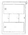
- FIG. 3 illustrates a power management module 700.
- Power management module 700 resides within memory controller 510 and manages the activity of DIMMs 520, 530 and 540.
- Power management module 700 includes device pools 710 and 750. Each of the memory device rows coupled to bus 501 are grouped into either pool 710 or pool 750. All rows that are grouped within pool 710 are in the ACTIVE/IDLE state. All rows that do not reside in pool 710 are grouped within pool 750. Thus, all rows that are in the POWERED DOWN state reside in pool 750. According to one embodiment, only one (1) row may reside in pool 710 at a time. However, the maximum number of rows that may reside in pool 710 may be programmed. In such an embodiment, a user of computer system 500 may program the maximum number of memory devices that may be grouped in pool 710.
- a row residing in pool 750 may only enter pool 710 when a memory device within the row is accessed by a memory request from memory controller 510. Additionally, a row is moved to pool 750 from pool 710 whenever another row needs to be moved from pool 750 into pool 710 and pool 710 is filled to capacity. In this case the LRU device in pool 710 is selected to be transferred to pool 750. Before the row is moved to pool 750 all open pages must first be closed. According to one embodiment, a timer is included within memory controller 510 that moves a row from pool 710 to pool 750 if a memory device within the row has not been accessed in a predetermined period of time.
- Figure 4 is a flow diagram of one embodiment with a process performed by power management module 700.
- process block 805 access to a memory device within one of the rows of memory unit 515 is requested.
- process block 810 it is determined at memory controller 510 whether the DIMM resides in pool 710. If it is determined that the row resides in pool 710, control is returned back to process block 805 wherein access to another memory device is requested. If it is determined that the row does not reside in pool 710, it is determined whether pool 710 is full, process block 815.
- pool 710 is full the LRU row in pool 710 is logically transferred to pool 750, process block 820.
- the requested row is logically moved from pool 750 to pool 710 and is switched to the ACTIVE/IDLE state. If pool 710 is not full the row is moved directly from pool 750 to pool 710 and is switched to the ACTIVE/IDLE state, process block 825.
- SLDRAMS Sync Link DRAMS
- EDO DRAMS etc.
Landscapes
- Engineering & Computer Science (AREA)
- Theoretical Computer Science (AREA)
- Physics & Mathematics (AREA)
- General Engineering & Computer Science (AREA)
- General Physics & Mathematics (AREA)
- Power Sources (AREA)
- Techniques For Improving Reliability Of Storages (AREA)
Claims (8)
- Verfahren zur Verwaltung von Energie, wobei das Verfahren folgendes umfasst:das Anfordern eines Zugriffs auf eine erste Speichervorrichtung in einer ersten Zeile einer Mehrzahl von Zeilen (520, 530, 540) in einem Dynamic Random Access Memory (DRAM) System, wobei jede Zeile eine Mehrzahl von Speichervorrichtungen (523, 533, 543) umfasst, wobei jede Zeile der genannten Mehrzahl von Zeilen als einer ersten Gruppe (710) oder einer zweiten Gruppe (750) zugehörig klassifiziert ist, wobei sich alle Zeilen in der genannten ersten Gruppe (710) in einem aktiven Leistungszustand befinden, und wobei sich alle Zeilen in der genannten zweiten Gruppe (750) in einem ausgeschalteten Leistungszustand befinden;das Bestimmen, ob die genannte erste Zeile als der genannten ersten Gruppe (710) zugehörig klassifiziert ist; wenn dies nicht der Fall ist, dann:das Bestimmten, ob die genannte erste Gruppe (710) bis auf eine Kapazität der ersten Gruppe gefüllt ist, und wenn dies nicht der Fall ist:das Übertragen der genannten ersten Zeile zu der genannten ersten Gruppe (710); unddas Begrenzen des Energieverbrauchs des DRAM-Systems durch die Begrenzung der Kapazität der ersten Gruppe (710).
- Verfahren nach Anspruch 1, wobei das Verfahren ferner das Übertragen einer zweiten Zeile von der ersten Gruppe (710) zu der zweiten Gruppe (750) umfasst, wenn die erste Gruppe (710) bis auf ihre Kapazität gefüllt ist.
- Verfahren nach Anspruch 1 oder 2, wobei die Kapazität der ersten Gruppe (710) programmierbar ist.
- Verfahren nach Anspruch 1, wobei das Verfahren ferner folgendes umfasst:das Übertragen einer zweiten Zeile von der ersten Gruppe (710) zu der zweiten Gruppe (750), wenn innerhalb eines vorbestimmten Zeitintervalls nicht auf die zweite Zeile zugegriffen worden ist.
- Verfahren nach Anspruch 2, wobei es sich bei der zweiten Zeile um die zuletzt genutzte Zeile in der ersten Gruppe handelt.
- Computersystem, das folgendes umfasst:ein Speichersystem mit einer Mehrzahl von Zeilen (520, 530, 540), wobei jede Zeile eine Mehrzahl von DRAM-Speichervorrichtungen (523, 533, 543) aufweist, und wobei die Speichervorrichtungen in jeder Zeile der Mehrzahl von Zeilen gemäß einem aktiven Leistungszustand oder einem ausgeschalteten Leistungszustand arbeiten, und gekennzeichnet durch:eine Speicherstetiereinheit (510), die so angeordnet ist, dass sie die Energie der Mehrzahl von Speichervorrichtungen (523, 533, 543) durch Identifizieren der Zeilen (520, 530, 540) von Speichervorrichtungen, die in dem aktiven Leistungszustand arbeiten, als einer ersten Gruppe (710) zugehörig verwaltet, und durch Identifizieren der Zeilen (520, 530, 540) von Speichervorrichtungen (523, 533, 543), die in dem ausgeschalteten Leistungszustand arbeiten, als einer zweiten Gruppe (750) zugehörig, und wobei eine erste Zeile, die eine Speichervorrichtung aufweist, auf die durch eine Speicheranforderung von der Speichersteuereinheit zugegriffen worden ist, zu der ersten Gruppe (710) übertragen wird, wenn die erste Gruppe ausreichende Kapazität für den Empfang der ersten Zeile aufweist;wobei die Kapazität der ersten Gruppe begrenzt ist, um den Energieverbrauch des Speichersystems zu begrenzen.
- Computersystem nach Anspruch 6, wobei eine erste Zeile von Speichervorrichtungen, die als der zweiten Gruppe (750) zugehörig identifiziert worden ist, nach dem Zugriff durch die Speiehersteuereinheit (510) zu der ersten Gruppe (710) übertragen wird.
- Computersystem nach Anspruch 6, wobei eine zweite Zeile von Speichervorrichtungen, die als der ersten Gruppe (710) zugehörig identifiziert worden ist, zu der zweiten Gruppe (750) übertragen wird, wenn die erste Gruppe (710) bis auf ihre Kapazität gefüllt ist.
Applications Claiming Priority (3)
| Application Number | Priority Date | Filing Date | Title |
|---|---|---|---|
| US09/187,565 US6442698B2 (en) | 1998-11-04 | 1998-11-04 | Method and apparatus for power management in a memory subsystem |
| US187565 | 1998-11-04 | ||
| PCT/US1999/025945 WO2000026755A1 (en) | 1998-11-04 | 1999-11-03 | Method and apparatus for power management in a memory subsystem |
Publications (3)
| Publication Number | Publication Date |
|---|---|
| EP1127308A1 EP1127308A1 (de) | 2001-08-29 |
| EP1127308A4 EP1127308A4 (de) | 2003-05-21 |
| EP1127308B1 true EP1127308B1 (de) | 2009-10-21 |
Family
ID=22689486
Family Applications (1)
| Application Number | Title | Priority Date | Filing Date |
|---|---|---|---|
| EP99971533A Expired - Lifetime EP1127308B1 (de) | 1998-11-04 | 1999-11-03 | Verfahren und gerät für leistungssteuerung in einem speicheruntersystem |
Country Status (9)
| Country | Link |
|---|---|
| US (2) | US20020124195A1 (de) |
| EP (1) | EP1127308B1 (de) |
| CN (1) | CN100430865C (de) |
| AU (1) | AU1466600A (de) |
| BR (1) | BR9915060A (de) |
| DE (1) | DE69941577D1 (de) |
| HK (1) | HK1036665A1 (de) |
| TW (1) | TW484051B (de) |
| WO (1) | WO2000026755A1 (de) |
Families Citing this family (67)
| Publication number | Priority date | Publication date | Assignee | Title |
|---|---|---|---|---|
| JP4265850B2 (ja) * | 2000-01-17 | 2009-05-20 | 富士通株式会社 | 移動体交換機、ホームメモリ・ノード装置および関門交換機 |
| US6633987B2 (en) * | 2000-03-24 | 2003-10-14 | Intel Corporation | Method and apparatus to implement the ACPI(advanced configuration and power interface) C3 state in a RDRAM based system |
| US6691237B1 (en) * | 2000-08-08 | 2004-02-10 | Dell Products, L.P. | Active memory pool management policies |
| US6925529B2 (en) * | 2001-07-12 | 2005-08-02 | International Business Machines Corporation | Data storage on a multi-tiered disk system |
| US6820169B2 (en) * | 2001-09-25 | 2004-11-16 | Intel Corporation | Memory control with lookahead power management |
| US20030097519A1 (en) * | 2001-11-21 | 2003-05-22 | Yoon Ha Ryong | Memory subsystem |
| US7103730B2 (en) * | 2002-04-09 | 2006-09-05 | Intel Corporation | Method, system, and apparatus for reducing power consumption of a memory |
| US7028200B2 (en) * | 2002-05-15 | 2006-04-11 | Broadcom Corporation | Method and apparatus for adaptive power management of memory subsystem |
| US7051174B2 (en) * | 2002-09-24 | 2006-05-23 | International Business Machines Corporation | Method, system, and program for restoring data in cache |
| US6853603B1 (en) * | 2004-03-09 | 2005-02-08 | Altera Corporation | Programmable logic device having nonvolatile memory with user selectable power consumption |
| US7272728B2 (en) * | 2004-06-14 | 2007-09-18 | Iovation, Inc. | Network security and fraud detection system and method |
| US7296129B2 (en) * | 2004-07-30 | 2007-11-13 | International Business Machines Corporation | System, method and storage medium for providing a serialized memory interface with a bus repeater |
| US7389375B2 (en) | 2004-07-30 | 2008-06-17 | International Business Machines Corporation | System, method and storage medium for a multi-mode memory buffer device |
| US20060036826A1 (en) * | 2004-07-30 | 2006-02-16 | International Business Machines Corporation | System, method and storage medium for providing a bus speed multiplier |
| US7224595B2 (en) | 2004-07-30 | 2007-05-29 | International Business Machines Corporation | 276-Pin buffered memory module with enhanced fault tolerance |
| US7512762B2 (en) | 2004-10-29 | 2009-03-31 | International Business Machines Corporation | System, method and storage medium for a memory subsystem with positional read data latency |
| US7305574B2 (en) * | 2004-10-29 | 2007-12-04 | International Business Machines Corporation | System, method and storage medium for bus calibration in a memory subsystem |
| US7277988B2 (en) * | 2004-10-29 | 2007-10-02 | International Business Machines Corporation | System, method and storage medium for providing data caching and data compression in a memory subsystem |
| US7356737B2 (en) | 2004-10-29 | 2008-04-08 | International Business Machines Corporation | System, method and storage medium for testing a memory module |
| US7299313B2 (en) * | 2004-10-29 | 2007-11-20 | International Business Machines Corporation | System, method and storage medium for a memory subsystem command interface |
| US7331010B2 (en) | 2004-10-29 | 2008-02-12 | International Business Machines Corporation | System, method and storage medium for providing fault detection and correction in a memory subsystem |
| US7395476B2 (en) | 2004-10-29 | 2008-07-01 | International Business Machines Corporation | System, method and storage medium for providing a high speed test interface to a memory subsystem |
| GB2426360A (en) * | 2005-05-18 | 2006-11-22 | Symbian Software Ltd | Reorganisation of memory for conserving power in a computing device |
| US8090897B2 (en) | 2006-07-31 | 2012-01-03 | Google Inc. | System and method for simulating an aspect of a memory circuit |
| US9171585B2 (en) | 2005-06-24 | 2015-10-27 | Google Inc. | Configurable memory circuit system and method |
| US9542352B2 (en) | 2006-02-09 | 2017-01-10 | Google Inc. | System and method for reducing command scheduling constraints of memory circuits |
| US8359187B2 (en) | 2005-06-24 | 2013-01-22 | Google Inc. | Simulating a different number of memory circuit devices |
| US8796830B1 (en) | 2006-09-01 | 2014-08-05 | Google Inc. | Stackable low-profile lead frame package |
| US7392338B2 (en) | 2006-07-31 | 2008-06-24 | Metaram, Inc. | Interface circuit system and method for autonomously performing power management operations in conjunction with a plurality of memory circuits |
| US9507739B2 (en) | 2005-06-24 | 2016-11-29 | Google Inc. | Configurable memory circuit system and method |
| US8438328B2 (en) | 2008-02-21 | 2013-05-07 | Google Inc. | Emulation of abstracted DIMMs using abstracted DRAMs |
| US8327104B2 (en) | 2006-07-31 | 2012-12-04 | Google Inc. | Adjusting the timing of signals associated with a memory system |
| US8077535B2 (en) | 2006-07-31 | 2011-12-13 | Google Inc. | Memory refresh apparatus and method |
| US10013371B2 (en) | 2005-06-24 | 2018-07-03 | Google Llc | Configurable memory circuit system and method |
| US8060774B2 (en) | 2005-06-24 | 2011-11-15 | Google Inc. | Memory systems and memory modules |
| US8081474B1 (en) | 2007-12-18 | 2011-12-20 | Google Inc. | Embossed heat spreader |
| US20080082763A1 (en) | 2006-10-02 | 2008-04-03 | Metaram, Inc. | Apparatus and method for power management of memory circuits by a system or component thereof |
| US8089795B2 (en) | 2006-02-09 | 2012-01-03 | Google Inc. | Memory module with memory stack and interface with enhanced capabilities |
| US8130560B1 (en) | 2006-11-13 | 2012-03-06 | Google Inc. | Multi-rank partial width memory modules |
| US7472220B2 (en) | 2006-07-31 | 2008-12-30 | Metaram, Inc. | Interface circuit system and method for performing power management operations utilizing power management signals |
| US8041881B2 (en) | 2006-07-31 | 2011-10-18 | Google Inc. | Memory device with emulated characteristics |
| US8397013B1 (en) | 2006-10-05 | 2013-03-12 | Google Inc. | Hybrid memory module |
| US8055833B2 (en) | 2006-10-05 | 2011-11-08 | Google Inc. | System and method for increasing capacity, performance, and flexibility of flash storage |
| US8386722B1 (en) | 2008-06-23 | 2013-02-26 | Google Inc. | Stacked DIMM memory interface |
| US7386656B2 (en) | 2006-07-31 | 2008-06-10 | Metaram, Inc. | Interface circuit system and method for performing power management operations in conjunction with only a portion of a memory circuit |
| US20080028136A1 (en) | 2006-07-31 | 2008-01-31 | Schakel Keith R | Method and apparatus for refresh management of memory modules |
| US8244971B2 (en) | 2006-07-31 | 2012-08-14 | Google Inc. | Memory circuit system and method |
| US7590796B2 (en) * | 2006-07-31 | 2009-09-15 | Metaram, Inc. | System and method for power management in memory systems |
| US8335894B1 (en) | 2008-07-25 | 2012-12-18 | Google Inc. | Configurable memory system with interface circuit |
| US8111566B1 (en) | 2007-11-16 | 2012-02-07 | Google, Inc. | Optimal channel design for memory devices for providing a high-speed memory interface |
| DE112006004263B4 (de) | 2005-09-02 | 2015-05-13 | Google, Inc. | Speicherbaustein |
| US7478259B2 (en) | 2005-10-31 | 2009-01-13 | International Business Machines Corporation | System, method and storage medium for deriving clocks in a memory system |
| US7685392B2 (en) | 2005-11-28 | 2010-03-23 | International Business Machines Corporation | Providing indeterminate read data latency in a memory system |
| US9632929B2 (en) | 2006-02-09 | 2017-04-25 | Google Inc. | Translating an address associated with a command communicated between a system and memory circuits |
| US7724589B2 (en) | 2006-07-31 | 2010-05-25 | Google Inc. | System and method for delaying a signal communicated from a system to at least one of a plurality of memory circuits |
| US7669086B2 (en) | 2006-08-02 | 2010-02-23 | International Business Machines Corporation | Systems and methods for providing collision detection in a memory system |
| US7490217B2 (en) | 2006-08-15 | 2009-02-10 | International Business Machines Corporation | Design structure for selecting memory busses according to physical memory organization information stored in virtual address translation tables |
| US7539842B2 (en) | 2006-08-15 | 2009-05-26 | International Business Machines Corporation | Computer memory system for selecting memory buses according to physical memory organization information stored in virtual address translation tables |
| US7870459B2 (en) * | 2006-10-23 | 2011-01-11 | International Business Machines Corporation | High density high reliability memory module with power gating and a fault tolerant address and command bus |
| US7721140B2 (en) | 2007-01-02 | 2010-05-18 | International Business Machines Corporation | Systems and methods for improving serviceability of a memory system |
| US8209479B2 (en) | 2007-07-18 | 2012-06-26 | Google Inc. | Memory circuit system and method |
| US8080874B1 (en) | 2007-09-14 | 2011-12-20 | Google Inc. | Providing additional space between an integrated circuit and a circuit board for positioning a component therebetween |
| US9105323B2 (en) * | 2009-01-23 | 2015-08-11 | Micron Technology, Inc. | Memory device power managers and methods |
| EP2441007A1 (de) | 2009-06-09 | 2012-04-18 | Google, Inc. | Programmierung von dimm-abschlusswiderstandswerten |
| US9368214B2 (en) | 2013-10-03 | 2016-06-14 | Apple Inc. | Programmable peak-current control in non-volatile memory devices |
| US10379748B2 (en) * | 2016-12-19 | 2019-08-13 | International Business Machines Corporation | Predictive scheduler for memory rank switching |
| CN111459261A (zh) * | 2020-04-03 | 2020-07-28 | 北京云宽志业网络技术有限公司 | 磁盘唤醒方法、装置、电子设备及存储介质 |
Family Cites Families (10)
| Publication number | Priority date | Publication date | Assignee | Title |
|---|---|---|---|---|
| JPH04143819A (ja) * | 1989-12-15 | 1992-05-18 | Hitachi Ltd | 消費電力制御方法、半導体集積回路装置およびマイクロプロセツサ |
| US5430683A (en) * | 1994-03-15 | 1995-07-04 | Intel Corporation | Method and apparatus for reducing power in on-chip tag SRAM |
| US5721860A (en) * | 1994-05-24 | 1998-02-24 | Intel Corporation | Memory controller for independently supporting synchronous and asynchronous DRAM memories |
| US5923829A (en) * | 1994-08-25 | 1999-07-13 | Ricoh Company, Ltd. | Memory system, memory control system and image processing system |
| US5598374A (en) * | 1995-07-14 | 1997-01-28 | Cirrus Logic, Inc. | Pipeland address memories, and systems and methods using the same |
| US5881016A (en) * | 1997-06-13 | 1999-03-09 | Cirrus Logic, Inc. | Method and apparatus for optimizing power consumption and memory bandwidth in a video controller using SGRAM and SDRAM power reduction modes |
| US5889714A (en) * | 1997-11-03 | 1999-03-30 | Digital Equipment Corporation | Adaptive precharge management for synchronous DRAM |
| US5835435A (en) * | 1997-12-02 | 1998-11-10 | Intel Corporation | Method and apparatus for dynamically placing portions of a memory in a reduced power consumtion state |
| US6003121A (en) * | 1998-05-18 | 1999-12-14 | Intel Corporation | Single and multiple channel memory detection and sizing |
| US6038673A (en) | 1998-11-03 | 2000-03-14 | Intel Corporation | Computer system with power management scheme for DRAM devices |
-
1998
- 1998-11-04 US US09/187,565 patent/US20020124195A1/en active Granted
- 1998-11-04 US US09/187,565 patent/US6442698B2/en not_active Expired - Lifetime
-
1999
- 1999-10-08 TW TW088117430A patent/TW484051B/zh not_active IP Right Cessation
- 1999-11-03 AU AU14666/00A patent/AU1466600A/en not_active Abandoned
- 1999-11-03 EP EP99971533A patent/EP1127308B1/de not_active Expired - Lifetime
- 1999-11-03 DE DE69941577T patent/DE69941577D1/de not_active Expired - Lifetime
- 1999-11-03 CN CNB998154164A patent/CN100430865C/zh not_active Expired - Fee Related
- 1999-11-03 WO PCT/US1999/025945 patent/WO2000026755A1/en active Application Filing
- 1999-11-03 BR BR9915060-3A patent/BR9915060A/pt not_active Application Discontinuation
-
2001
- 2001-10-29 HK HK01107539.2A patent/HK1036665A1/xx not_active IP Right Cessation
Also Published As
| Publication number | Publication date |
|---|---|
| US6442698B2 (en) | 2002-08-27 |
| HK1036665A1 (en) | 2002-01-11 |
| US20020124195A1 (en) | 2002-09-05 |
| DE69941577D1 (de) | 2009-12-03 |
| WO2000026755A1 (en) | 2000-05-11 |
| TW484051B (en) | 2002-04-21 |
| CN1332864A (zh) | 2002-01-23 |
| BR9915060A (pt) | 2001-08-07 |
| CN100430865C (zh) | 2008-11-05 |
| EP1127308A4 (de) | 2003-05-21 |
| EP1127308A1 (de) | 2001-08-29 |
| AU1466600A (en) | 2000-05-22 |
Similar Documents
| Publication | Publication Date | Title |
|---|---|---|
| EP1127308B1 (de) | Verfahren und gerät für leistungssteuerung in einem speicheruntersystem | |
| EP1192525B1 (de) | Verfahren und vorrichtung zur dynamischen änderung der grössen von pools, die die leistungsaufnahme von speichern steuern | |
| US7821864B2 (en) | Power management of memory via wake/sleep cycles | |
| US7353329B2 (en) | Memory buffer device integrating refresh logic | |
| US6327664B1 (en) | Power management on a memory card having a signal processing element | |
| EP1442355B1 (de) | Leistungssteuerung für dram | |
| CN1926519B (zh) | 用于节能的统一存储器组织 | |
| EP2761620B1 (de) | Dynamische operationen für gestapelte 3d speicher unter verwendung von wärmedaten | |
| WO2000026752A1 (en) | Computer system with power management scheme for dram devices | |
| CN101111814A (zh) | 多核架构中的工作点管理 | |
| US8438358B1 (en) | System-on-chip with memory speed control core | |
| US7650472B2 (en) | Method for reducing memory power consumption | |
| CN115516563A (zh) | 用于dram的刷新管理 | |
| US10572183B2 (en) | Power efficient retraining of memory accesses | |
| WO2022212100A1 (en) | Credit scheme for multi-queue memory controllers | |
| EP3945424B1 (de) | Speicherleistungsverwaltungsverfahren und prozessorsystem | |
| US11934251B2 (en) | Data fabric clock switching | |
| WO2022212089A1 (en) | Memory controller power states | |
| US20240004560A1 (en) | Efficient memory power control operations | |
| JP2001101067A (ja) | セルフ・リフレッシュ制御装置及びプログラムを記憶した記憶媒体 | |
| WO2022046689A1 (en) | Apparatus and methods for synchronizing a plurality of double data rate memory ranks |
Legal Events
| Date | Code | Title | Description |
|---|---|---|---|
| PUAI | Public reference made under article 153(3) epc to a published international application that has entered the european phase |
Free format text: ORIGINAL CODE: 0009012 |
|
| 17P | Request for examination filed |
Effective date: 20010523 |
|
| AK | Designated contracting states |
Kind code of ref document: A1 Designated state(s): AT BE CH CY DE DK ES FI FR GB GR IE IT LI LU MC NL PT SE |
|
| A4 | Supplementary search report drawn up and despatched |
Effective date: 20030409 |
|
| RBV | Designated contracting states (corrected) |
Designated state(s): DE FR GB |
|
| 17Q | First examination report despatched |
Effective date: 20050208 |
|
| 17Q | First examination report despatched |
Effective date: 20050208 |
|
| GRAP | Despatch of communication of intention to grant a patent |
Free format text: ORIGINAL CODE: EPIDOSNIGR1 |
|
| GRAS | Grant fee paid |
Free format text: ORIGINAL CODE: EPIDOSNIGR3 |
|
| GRAA | (expected) grant |
Free format text: ORIGINAL CODE: 0009210 |
|
| AK | Designated contracting states |
Kind code of ref document: B1 Designated state(s): DE FR GB |
|
| REG | Reference to a national code |
Ref country code: GB Ref legal event code: FG4D |
|
| REF | Corresponds to: |
Ref document number: 69941577 Country of ref document: DE Date of ref document: 20091203 Kind code of ref document: P |
|
| REG | Reference to a national code |
Ref country code: HK Ref legal event code: GR Ref document number: 1036665 Country of ref document: HK |
|
| PLBE | No opposition filed within time limit |
Free format text: ORIGINAL CODE: 0009261 |
|
| STAA | Information on the status of an ep patent application or granted ep patent |
Free format text: STATUS: NO OPPOSITION FILED WITHIN TIME LIMIT |
|
| 26N | No opposition filed |
Effective date: 20100722 |
|
| PGFP | Annual fee paid to national office [announced via postgrant information from national office to epo] |
Ref country code: FR Payment date: 20101202 Year of fee payment: 12 |
|
| REG | Reference to a national code |
Ref country code: FR Ref legal event code: ST Effective date: 20120731 |
|
| PG25 | Lapsed in a contracting state [announced via postgrant information from national office to epo] |
Ref country code: FR Free format text: LAPSE BECAUSE OF NON-PAYMENT OF DUE FEES Effective date: 20111130 |
|
| PGFP | Annual fee paid to national office [announced via postgrant information from national office to epo] |
Ref country code: DE Payment date: 20141029 Year of fee payment: 16 Ref country code: GB Payment date: 20141029 Year of fee payment: 16 |
|
| REG | Reference to a national code |
Ref country code: DE Ref legal event code: R119 Ref document number: 69941577 Country of ref document: DE |
|
| GBPC | Gb: european patent ceased through non-payment of renewal fee |
Effective date: 20151103 |
|
| PG25 | Lapsed in a contracting state [announced via postgrant information from national office to epo] |
Ref country code: GB Free format text: LAPSE BECAUSE OF NON-PAYMENT OF DUE FEES Effective date: 20151103 Ref country code: DE Free format text: LAPSE BECAUSE OF NON-PAYMENT OF DUE FEES Effective date: 20160601 |