EP1127308B1 - Method and apparatus for power management in a memory subsystem - Google Patents
Method and apparatus for power management in a memory subsystem Download PDFInfo
- Publication number
- EP1127308B1 EP1127308B1 EP99971533A EP99971533A EP1127308B1 EP 1127308 B1 EP1127308 B1 EP 1127308B1 EP 99971533 A EP99971533 A EP 99971533A EP 99971533 A EP99971533 A EP 99971533A EP 1127308 B1 EP1127308 B1 EP 1127308B1
- Authority
- EP
- European Patent Office
- Prior art keywords
- group
- row
- memory
- rows
- pool
- Prior art date
- Legal status (The legal status is an assumption and is not a legal conclusion. Google has not performed a legal analysis and makes no representation as to the accuracy of the status listed.)
- Expired - Lifetime
Links
Images


Classifications
-
- G—PHYSICS
- G06—COMPUTING; CALCULATING OR COUNTING
- G06F—ELECTRIC DIGITAL DATA PROCESSING
- G06F1/00—Details not covered by groups G06F3/00 - G06F13/00 and G06F21/00
- G06F1/26—Power supply means, e.g. regulation thereof
- G06F1/32—Means for saving power
- G06F1/3203—Power management, i.e. event-based initiation of a power-saving mode
- G06F1/3206—Monitoring of events, devices or parameters that trigger a change in power modality
- G06F1/3215—Monitoring of peripheral devices
- G06F1/3225—Monitoring of peripheral devices of memory devices
-
- G—PHYSICS
- G06—COMPUTING; CALCULATING OR COUNTING
- G06F—ELECTRIC DIGITAL DATA PROCESSING
- G06F1/00—Details not covered by groups G06F3/00 - G06F13/00 and G06F21/00
- G06F1/26—Power supply means, e.g. regulation thereof
- G06F1/32—Means for saving power
- G06F1/3203—Power management, i.e. event-based initiation of a power-saving mode
- G06F1/3234—Power saving characterised by the action undertaken
- G06F1/325—Power saving in peripheral device
- G06F1/3275—Power saving in memory, e.g. RAM, cache
-
- G—PHYSICS
- G06—COMPUTING; CALCULATING OR COUNTING
- G06F—ELECTRIC DIGITAL DATA PROCESSING
- G06F12/00—Accessing, addressing or allocating within memory systems or architectures
- G06F12/02—Addressing or allocation; Relocation
- G06F12/06—Addressing a physical block of locations, e.g. base addressing, module addressing, memory dedication
-
- Y—GENERAL TAGGING OF NEW TECHNOLOGICAL DEVELOPMENTS; GENERAL TAGGING OF CROSS-SECTIONAL TECHNOLOGIES SPANNING OVER SEVERAL SECTIONS OF THE IPC; TECHNICAL SUBJECTS COVERED BY FORMER USPC CROSS-REFERENCE ART COLLECTIONS [XRACs] AND DIGESTS
- Y02—TECHNOLOGIES OR APPLICATIONS FOR MITIGATION OR ADAPTATION AGAINST CLIMATE CHANGE
- Y02D—CLIMATE CHANGE MITIGATION TECHNOLOGIES IN INFORMATION AND COMMUNICATION TECHNOLOGIES [ICT], I.E. INFORMATION AND COMMUNICATION TECHNOLOGIES AIMING AT THE REDUCTION OF THEIR OWN ENERGY USE
- Y02D10/00—Energy efficient computing, e.g. low power processors, power management or thermal management
Definitions
- the present invention relates to system memory power management in a computer system; more particularly, the present invention relates to power management in memory subsystems.
- SDRAMs Synchronous Dynamic Random Access Memories
- typical SDRAMs operate at speeds up to 66Mhz.
- the power generated by SDRAMs operating at such speeds is relatively low.
- RDRAMs Rambus Dynamic Random Access Memories
- SDRAMs are capable of operating at speeds up to 100Mhz, while RDRAMs operate at clock speeds up to 400Mhz and transfer rate up to 800 MHz.
- Memory devices operating at such high speed result in a significant amount of power being generated within the device (e.g., on the order of 2.1 watts for RDRAMs). The generation of this magnitude of power may potentially create thermal issues at the memory device.
- WO 00/26752 which has an earlier priority date than the present application but a publication date which is after the priority date of the present application, discloses a computer system employing DRAM devices which are assigned into particular pools corresponding to different power consumption states with a most recently accessed device being assigned to an active pool and placed at the top of a stack structure.
- a least recently accessed device in the active pool is evicted from the pool and placed in a standby pool when the active pool is full and the processor accesses another device which is not currently assigned to the active pool.
- a least recently active device of the standby pool is evicted into a nap pool when either a time-out occurs or the standby and active pools are full and the processors accesses another device which is not currently assigned to either the active or standby pools.
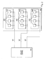
- FIG. 1 is a block diagram of one embodiment of a computer system 500.
- Computer system 500 includes a bus 501, a memory controller 510, a memory unit 515 and CPU 105. As described above, CPU 105 processes information received from memory 515 or other internal and external devices of computer system 500.
- Memory controller 510 is coupled to CPU 105. Memory controller 510 interfaces with memory unit 515 in order to carry out memory transactions.
- Memory unit 515 is coupled to memory controller 110 via bus 501.
- memory unit 515 is a Synchronous Dynamic Access Memory (SDRAM).
- SDRAM Synchronous Dynamic Access Memory
- An SDRAM is a form of DRAM that can be coordinated or synchronized to the clock speed of CPU 105.
- Bus 501 is a DRAM bus that permits memory controller 510 to communicate with memory unit 515. Bus 501 operates at speeds up to 133 MHz.
- Memory unit 515 includes Dual In-line Memory Modules (DIMMs) 520, 530 and 540.
- DIMMs 520, 530 and 540 include memory devices 523, 533 and 543, respectively, that are accessed by CPU 105 or other devices in order to store or read data.
- a DIMM may include one or more rows of memory. Each row within a DIMM is coupled to memory controller 510 by bus 501.
- Figure 2 illustrates a logical representation of the interface between memory controller 510 and memory unit 515 wherein DIMMs 520, 530 and 540 constitute separate rows of memory devices within memory unit 515.
- each row within memory unit 515 operates according to either an ACTIVE/IDLE state or POWERED DOWN state.
- a row is in the ACTIVE/IDLE state whenever a memory device within the DIMM is ready to transfer, or is actually transferring data.
- a row is in the POWERED DOWN state whenever no memory device within the row has been accessed for a long period of time.
- Bus 501 is received at the input of row 520 and is coupled to each of the memory devices 523.
- bus 501 is received at the input of DIMM 530 and is coupled to each memory device 533.
- bus 501 is received at that input DIMM 540 and is coupled to each memory device 543.
- memory unit 515 includes three rows of DIMS (e.g., DIMMs 520, 530 and 540). However, one of ordinary skill in the art will appreciate that additional DIMMs may be added to memory unit 515.
- each of the DIMMs includes four (4) memory devices. Therefore, four memory devices are included in each row coupled to bus 501.
- DIMMs 520, 530 and 540 may each include a different number of memory devices, as well as different combinations.
- DIMM 520 may include sixteen (16) memory devices 523
- DIMMs 530 and 540 may each include eight (8) memory devices 533 and 543, respectively.
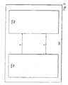
- FIG. 3 illustrates a power management module 700.
- Power management module 700 resides within memory controller 510 and manages the activity of DIMMs 520, 530 and 540.
- Power management module 700 includes device pools 710 and 750. Each of the memory device rows coupled to bus 501 are grouped into either pool 710 or pool 750. All rows that are grouped within pool 710 are in the ACTIVE/IDLE state. All rows that do not reside in pool 710 are grouped within pool 750. Thus, all rows that are in the POWERED DOWN state reside in pool 750. According to one embodiment, only one (1) row may reside in pool 710 at a time. However, the maximum number of rows that may reside in pool 710 may be programmed. In such an embodiment, a user of computer system 500 may program the maximum number of memory devices that may be grouped in pool 710.
- a row residing in pool 750 may only enter pool 710 when a memory device within the row is accessed by a memory request from memory controller 510. Additionally, a row is moved to pool 750 from pool 710 whenever another row needs to be moved from pool 750 into pool 710 and pool 710 is filled to capacity. In this case the LRU device in pool 710 is selected to be transferred to pool 750. Before the row is moved to pool 750 all open pages must first be closed. According to one embodiment, a timer is included within memory controller 510 that moves a row from pool 710 to pool 750 if a memory device within the row has not been accessed in a predetermined period of time.
- Figure 4 is a flow diagram of one embodiment with a process performed by power management module 700.
- process block 805 access to a memory device within one of the rows of memory unit 515 is requested.
- process block 810 it is determined at memory controller 510 whether the DIMM resides in pool 710. If it is determined that the row resides in pool 710, control is returned back to process block 805 wherein access to another memory device is requested. If it is determined that the row does not reside in pool 710, it is determined whether pool 710 is full, process block 815.
- pool 710 is full the LRU row in pool 710 is logically transferred to pool 750, process block 820.
- the requested row is logically moved from pool 750 to pool 710 and is switched to the ACTIVE/IDLE state. If pool 710 is not full the row is moved directly from pool 750 to pool 710 and is switched to the ACTIVE/IDLE state, process block 825.
- SLDRAMS Sync Link DRAMS
- EDO DRAMS etc.
Description
- The present invention relates to system memory power management in a computer system; more particularly, the present invention relates to power management in memory subsystems.
- Traditionally, the power generated by memory chips, in particularly, Synchronous Dynamic Random Access Memories (SDRAMs) was of little concern because of the low speeds at which they operate. For example, typical SDRAMs operate at speeds up to 66Mhz. The power generated by SDRAMs operating at such speeds is relatively low. However, with the increase of the operating speeds of SDRAMs and the advent of the Rambus Dynamic Random Access Memories (RDRAMs), operating speeds have dramatically increased. Presently, SDRAMs are capable of operating at speeds up to 100Mhz, while RDRAMs operate at clock speeds up to 400Mhz and transfer rate up to 800 MHz. Memory devices operating at such high speed result in a significant amount of power being generated within the device (e.g., on the order of 2.1 watts for RDRAMs). The generation of this magnitude of power may potentially create thermal issues at the memory device.
- One current method of remedying the excessive generation of power is by curtailing the bandwidth of a memory. This solution is disadvantageous since it decreases the performance of the memory. Another solution is to use heatsinks and/or cooling fans with memory chips to decrease the heat generated by a memory operating at high speeds. However, this method is disadvantageous because of the cost and amount of space that is consumed by such devices.
WO 00/26752 - According to a first aspect of this invention there is provided a power management method as claimed in claim 1 herein.
- According to a second aspect of this invention there is provided a computer system as claimed in claim 6 herein.
- Further features of this invention are defined by the dependent claims.
- The present invention will be understood more fully from the detailed description given below and from the accompanying drawings of various embodiments of the invention. The drawings, however, should not be taken to limit the invention to the specific embodiments, but are for explanation and understanding only.
-
Figure 1 is a block diagram of one embodiment of a computer system; -
Figure 2 is a block diagram of a logical representation of a memory controller interface in accordance with one embodiment of the present invention; -
Figure 3 is a power management module in accordance with one embodiment of the present invention; and -
Figure 4 is a flow diagram of the operation of one embodiment of a power management module. -
Figure 1 is a block diagram of one embodiment of acomputer system 500.Computer system 500 includes abus 501, amemory controller 510, amemory unit 515 andCPU 105. As described above,CPU 105 processes information received frommemory 515 or other internal and external devices ofcomputer system 500.Memory controller 510 is coupled toCPU 105.Memory controller 510 interfaces withmemory unit 515 in order to carry out memory transactions. -
Memory unit 515 is coupled to memory controller 110 viabus 501. According to one embodiment,memory unit 515 is a Synchronous Dynamic Access Memory (SDRAM). An SDRAM is a form of DRAM that can be coordinated or synchronized to the clock speed ofCPU 105.Bus 501 is a DRAM bus that permitsmemory controller 510 to communicate withmemory unit 515.Bus 501 operates at speeds up to 133 MHz. -
Memory unit 515 includes Dual In-line Memory Modules (DIMMs) 520, 530 and 540.DIMMs memory devices CPU 105 or other devices in order to store or read data. A DIMM may include one or more rows of memory. Each row within a DIMM is coupled tomemory controller 510 bybus 501. For example,Figure 2 illustrates a logical representation of the interface betweenmemory controller 510 andmemory unit 515 whereinDIMMs memory unit 515. Additionally, each row withinmemory unit 515 operates according to either an ACTIVE/IDLE state or POWERED DOWN state. A row is in the ACTIVE/IDLE state whenever a memory device within the DIMM is ready to transfer, or is actually transferring data. A row is in the POWERED DOWN state whenever no memory device within the row has been accessed for a long period of time. -
Bus 501 is received at the input ofrow 520 and is coupled to each of thememory devices 523. In addition,bus 501 is received at the input of DIMM 530 and is coupled to eachmemory device 533. Further,bus 501 is received at thatinput DIMM 540 and is coupled to eachmemory device 543. According to one embodiment,memory unit 515 includes three rows of DIMS (e.g., DIMMs 520, 530 and 540). However, one of ordinary skill in the art will appreciate that additional DIMMs may be added tomemory unit 515. - According to a further embodiment, each of the DIMMs includes four (4) memory devices. Therefore, four memory devices are included in each row coupled to
bus 501. Nevertheless, one of ordinary skill in the art will appreciate that DIMMs 520, 530 and 540 may each include a different number of memory devices, as well as different combinations. For example, DIMM 520 may include sixteen (16)memory devices 523 and DIMMs 530 and 540 may each include eight (8)memory devices - The total power generated by a DIMM will be very high if all of the memory devices are in the ACTIVE/IDLE state.
Figure 3 illustrates apower management module 700.Power management module 700 resides withinmemory controller 510 and manages the activity of DIMMs 520, 530 and 540. -
Power management module 700 includesdevice pools 710 and 750. Each of the memory device rows coupled tobus 501 are grouped into eitherpool 710 or pool 750. All rows that are grouped withinpool 710 are in the ACTIVE/IDLE state. All rows that do not reside inpool 710 are grouped within pool 750. Thus, all rows that are in the POWERED DOWN state reside in pool 750. According to one embodiment, only one (1) row may reside inpool 710 at a time. However, the maximum number of rows that may reside inpool 710 may be programmed. In such an embodiment, a user ofcomputer system 500 may program the maximum number of memory devices that may be grouped inpool 710. - At the startup of
computer system 500 all rows are logically arranged into pool 750. A row residing in pool 750 may only enterpool 710 when a memory device within the row is accessed by a memory request frommemory controller 510. Additionally, a row is moved to pool 750 frompool 710 whenever another row needs to be moved from pool 750 intopool 710 andpool 710 is filled to capacity. In this case the LRU device inpool 710 is selected to be transferred to pool 750. Before the row is moved to pool 750 all open pages must first be closed. According to one embodiment, a timer is included withinmemory controller 510 that moves a row frompool 710 to pool 750 if a memory device within the row has not been accessed in a predetermined period of time. -
Figure 4 is a flow diagram of one embodiment with a process performed bypower management module 700. Atprocess block 805, access to a memory device within one of the rows ofmemory unit 515 is requested. Next, at process block 810 it is determined atmemory controller 510 whether the DIMM resides inpool 710. If it is determined that the row resides inpool 710, control is returned back to process block 805 wherein access to another memory device is requested. If it is determined that the row does not reside inpool 710, it is determined whetherpool 710 is full,process block 815. - If
pool 710 is full the LRU row inpool 710 is logically transferred to pool 750,process block 820. Atprocess block 825, the requested row is logically moved from pool 750 to pool 710 and is switched to the ACTIVE/IDLE state. Ifpool 710 is not full the row is moved directly from pool 750 to pool 710 and is switched to the ACTIVE/IDLE state,process block 825. One of ordinary skill in the art will appreciate that the present invention may be implemented in other memory systems, such as Sync Link DRAMS (SLDRAMS), EDO DRAMS etc. - Thus a method and apparatus for memory power management has been described
Claims (8)
- A power management method comprising:requesting access to a first memory device in a first row of a plurality of rows (520, 530, 540) in a Dynamic Random Access Memory (DRAM) system, each row comprising a plurality of memory devices (523, 533, 543), wherein each of said plurality of rows is classified as belonging to a first group (710) or a second group (750), wherein all rows within said first group (710) are in an active power state and all rows within said second group (750) are in a powered-down power state;determining if said first row is classified as belonging to said first group (710); if notdetermining if said first group (710) is filled to a capacity of the first group; and, if nottransferring said first row to said first group (710); andlimiting power consumption of the DRAM system by limiting the capacity of the first group (710).
- The method of claim 1 further comprising transferring a second row from the first group (710) to the second group (750) if the first group (710) is filled to capacity.
- The method of claims 1 or 2, wherein the capacity of the first group (710) is programmable.
- The method of claim 1 further comprising:transferring a second row from the first group (710) to the second group (750) if the second row has not been accessed in a predetermined interval of time.
- The method of claim 2, wherein the second row is the least recently used in the first group.
- A computer system comprising:a memory system including a plurality of rows (520, 530, 540), wherein each row includes a plurality of DRAM memory devices (523, 533, 543), and wherein the memory devices in each of the plurality of rows operate according to an active power state or a powered-down power state; and characterised bya memory controller (510) arranged to manage the power of the plurality of memory devices (523, 533, 543) by identifying rows (520, 530, 540) of memory devices operating in the active power state as belonging to a first group (710) and identifying rows (520, 530, 540) of memory devices (523, 533, 543) operating in the powered-down power state as belonging to a second group (750), and transferring a first row containing a memory device accessed by a memory request from the memory controller to the first group (710) if the first group has sufficient capacity to receive the first row;wherein the capacity of the first group is limited to limit power consumption of the memory system.
- The computer system of claim 6, wherein a first row of memory devices identified as belonging to the second group (750) is transferred to the first group (710) upon being accessed by the memory controller (510).
- The computer system of claim 6, wherein a second row of memory devices identified as belonging to the first group (710) is transferred to the second group (750) if the first group (710) is filled to capacity.
Applications Claiming Priority (3)
| Application Number | Priority Date | Filing Date | Title |
|---|---|---|---|
| US09/187,565 US6442698B2 (en) | 1998-11-04 | 1998-11-04 | Method and apparatus for power management in a memory subsystem |
| PCT/US1999/025945 WO2000026755A1 (en) | 1998-11-04 | 1999-11-03 | Method and apparatus for power management in a memory subsystem |
| US187565 | 2000-03-07 |
Publications (3)
| Publication Number | Publication Date |
|---|---|
| EP1127308A1 EP1127308A1 (en) | 2001-08-29 |
| EP1127308A4 EP1127308A4 (en) | 2003-05-21 |
| EP1127308B1 true EP1127308B1 (en) | 2009-10-21 |
Family
ID=22689486
Family Applications (1)
| Application Number | Title | Priority Date | Filing Date |
|---|---|---|---|
| EP99971533A Expired - Lifetime EP1127308B1 (en) | 1998-11-04 | 1999-11-03 | Method and apparatus for power management in a memory subsystem |
Country Status (9)
| Country | Link |
|---|---|
| US (2) | US6442698B2 (en) |
| EP (1) | EP1127308B1 (en) |
| CN (1) | CN100430865C (en) |
| AU (1) | AU1466600A (en) |
| BR (1) | BR9915060A (en) |
| DE (1) | DE69941577D1 (en) |
| HK (1) | HK1036665A1 (en) |
| TW (1) | TW484051B (en) |
| WO (1) | WO2000026755A1 (en) |
Families Citing this family (67)
| Publication number | Priority date | Publication date | Assignee | Title |
|---|---|---|---|---|
| JP4265850B2 (en) * | 2000-01-17 | 2009-05-20 | 富士通株式会社 | Mobile switch, home memory node device, and gateway switch |
| US6633987B2 (en) * | 2000-03-24 | 2003-10-14 | Intel Corporation | Method and apparatus to implement the ACPI(advanced configuration and power interface) C3 state in a RDRAM based system |
| US6691237B1 (en) * | 2000-08-08 | 2004-02-10 | Dell Products, L.P. | Active memory pool management policies |
| US6925529B2 (en) * | 2001-07-12 | 2005-08-02 | International Business Machines Corporation | Data storage on a multi-tiered disk system |
| US6820169B2 (en) * | 2001-09-25 | 2004-11-16 | Intel Corporation | Memory control with lookahead power management |
| US20030097519A1 (en) * | 2001-11-21 | 2003-05-22 | Yoon Ha Ryong | Memory subsystem |
| US7103730B2 (en) * | 2002-04-09 | 2006-09-05 | Intel Corporation | Method, system, and apparatus for reducing power consumption of a memory |
| US7028200B2 (en) * | 2002-05-15 | 2006-04-11 | Broadcom Corporation | Method and apparatus for adaptive power management of memory subsystem |
| US7051174B2 (en) * | 2002-09-24 | 2006-05-23 | International Business Machines Corporation | Method, system, and program for restoring data in cache |
| US6853603B1 (en) * | 2004-03-09 | 2005-02-08 | Altera Corporation | Programmable logic device having nonvolatile memory with user selectable power consumption |
| US7272728B2 (en) * | 2004-06-14 | 2007-09-18 | Iovation, Inc. | Network security and fraud detection system and method |
| US7296129B2 (en) | 2004-07-30 | 2007-11-13 | International Business Machines Corporation | System, method and storage medium for providing a serialized memory interface with a bus repeater |
| US20060036826A1 (en) * | 2004-07-30 | 2006-02-16 | International Business Machines Corporation | System, method and storage medium for providing a bus speed multiplier |
| US7224595B2 (en) | 2004-07-30 | 2007-05-29 | International Business Machines Corporation | 276-Pin buffered memory module with enhanced fault tolerance |
| US7389375B2 (en) * | 2004-07-30 | 2008-06-17 | International Business Machines Corporation | System, method and storage medium for a multi-mode memory buffer device |
| US7277988B2 (en) * | 2004-10-29 | 2007-10-02 | International Business Machines Corporation | System, method and storage medium for providing data caching and data compression in a memory subsystem |
| US7305574B2 (en) * | 2004-10-29 | 2007-12-04 | International Business Machines Corporation | System, method and storage medium for bus calibration in a memory subsystem |
| US7512762B2 (en) | 2004-10-29 | 2009-03-31 | International Business Machines Corporation | System, method and storage medium for a memory subsystem with positional read data latency |
| US7331010B2 (en) | 2004-10-29 | 2008-02-12 | International Business Machines Corporation | System, method and storage medium for providing fault detection and correction in a memory subsystem |
| US7356737B2 (en) | 2004-10-29 | 2008-04-08 | International Business Machines Corporation | System, method and storage medium for testing a memory module |
| US7299313B2 (en) * | 2004-10-29 | 2007-11-20 | International Business Machines Corporation | System, method and storage medium for a memory subsystem command interface |
| US7395476B2 (en) | 2004-10-29 | 2008-07-01 | International Business Machines Corporation | System, method and storage medium for providing a high speed test interface to a memory subsystem |
| GB2426360A (en) * | 2005-05-18 | 2006-11-22 | Symbian Software Ltd | Reorganisation of memory for conserving power in a computing device |
| US7386656B2 (en) | 2006-07-31 | 2008-06-10 | Metaram, Inc. | Interface circuit system and method for performing power management operations in conjunction with only a portion of a memory circuit |
| US7472220B2 (en) | 2006-07-31 | 2008-12-30 | Metaram, Inc. | Interface circuit system and method for performing power management operations utilizing power management signals |
| US8327104B2 (en) | 2006-07-31 | 2012-12-04 | Google Inc. | Adjusting the timing of signals associated with a memory system |
| US8089795B2 (en) | 2006-02-09 | 2012-01-03 | Google Inc. | Memory module with memory stack and interface with enhanced capabilities |
| US8060774B2 (en) | 2005-06-24 | 2011-11-15 | Google Inc. | Memory systems and memory modules |
| US8041881B2 (en) | 2006-07-31 | 2011-10-18 | Google Inc. | Memory device with emulated characteristics |
| US9171585B2 (en) | 2005-06-24 | 2015-10-27 | Google Inc. | Configurable memory circuit system and method |
| US8111566B1 (en) | 2007-11-16 | 2012-02-07 | Google, Inc. | Optimal channel design for memory devices for providing a high-speed memory interface |
| US8386722B1 (en) | 2008-06-23 | 2013-02-26 | Google Inc. | Stacked DIMM memory interface |
| US8055833B2 (en) | 2006-10-05 | 2011-11-08 | Google Inc. | System and method for increasing capacity, performance, and flexibility of flash storage |
| US7392338B2 (en) | 2006-07-31 | 2008-06-24 | Metaram, Inc. | Interface circuit system and method for autonomously performing power management operations in conjunction with a plurality of memory circuits |
| US8438328B2 (en) | 2008-02-21 | 2013-05-07 | Google Inc. | Emulation of abstracted DIMMs using abstracted DRAMs |
| US8077535B2 (en) | 2006-07-31 | 2011-12-13 | Google Inc. | Memory refresh apparatus and method |
| US8130560B1 (en) | 2006-11-13 | 2012-03-06 | Google Inc. | Multi-rank partial width memory modules |
| US8244971B2 (en) | 2006-07-31 | 2012-08-14 | Google Inc. | Memory circuit system and method |
| US9542352B2 (en) | 2006-02-09 | 2017-01-10 | Google Inc. | System and method for reducing command scheduling constraints of memory circuits |
| US8796830B1 (en) | 2006-09-01 | 2014-08-05 | Google Inc. | Stackable low-profile lead frame package |
| US20080028136A1 (en) | 2006-07-31 | 2008-01-31 | Schakel Keith R | Method and apparatus for refresh management of memory modules |
| US9507739B2 (en) | 2005-06-24 | 2016-11-29 | Google Inc. | Configurable memory circuit system and method |
| US20080082763A1 (en) | 2006-10-02 | 2008-04-03 | Metaram, Inc. | Apparatus and method for power management of memory circuits by a system or component thereof |
| US8359187B2 (en) | 2005-06-24 | 2013-01-22 | Google Inc. | Simulating a different number of memory circuit devices |
| US8090897B2 (en) | 2006-07-31 | 2012-01-03 | Google Inc. | System and method for simulating an aspect of a memory circuit |
| US7590796B2 (en) * | 2006-07-31 | 2009-09-15 | Metaram, Inc. | System and method for power management in memory systems |
| US8081474B1 (en) | 2007-12-18 | 2011-12-20 | Google Inc. | Embossed heat spreader |
| US10013371B2 (en) | 2005-06-24 | 2018-07-03 | Google Llc | Configurable memory circuit system and method |
| US8397013B1 (en) | 2006-10-05 | 2013-03-12 | Google Inc. | Hybrid memory module |
| US8335894B1 (en) | 2008-07-25 | 2012-12-18 | Google Inc. | Configurable memory system with interface circuit |
| GB2444663B (en) | 2005-09-02 | 2011-12-07 | Metaram Inc | Methods and apparatus of stacking drams |
| US7478259B2 (en) | 2005-10-31 | 2009-01-13 | International Business Machines Corporation | System, method and storage medium for deriving clocks in a memory system |
| US7685392B2 (en) | 2005-11-28 | 2010-03-23 | International Business Machines Corporation | Providing indeterminate read data latency in a memory system |
| US9632929B2 (en) | 2006-02-09 | 2017-04-25 | Google Inc. | Translating an address associated with a command communicated between a system and memory circuits |
| US7724589B2 (en) | 2006-07-31 | 2010-05-25 | Google Inc. | System and method for delaying a signal communicated from a system to at least one of a plurality of memory circuits |
| US7669086B2 (en) | 2006-08-02 | 2010-02-23 | International Business Machines Corporation | Systems and methods for providing collision detection in a memory system |
| US7539842B2 (en) | 2006-08-15 | 2009-05-26 | International Business Machines Corporation | Computer memory system for selecting memory buses according to physical memory organization information stored in virtual address translation tables |
| US7490217B2 (en) | 2006-08-15 | 2009-02-10 | International Business Machines Corporation | Design structure for selecting memory busses according to physical memory organization information stored in virtual address translation tables |
| US7870459B2 (en) * | 2006-10-23 | 2011-01-11 | International Business Machines Corporation | High density high reliability memory module with power gating and a fault tolerant address and command bus |
| US7721140B2 (en) | 2007-01-02 | 2010-05-18 | International Business Machines Corporation | Systems and methods for improving serviceability of a memory system |
| US8209479B2 (en) | 2007-07-18 | 2012-06-26 | Google Inc. | Memory circuit system and method |
| US8080874B1 (en) | 2007-09-14 | 2011-12-20 | Google Inc. | Providing additional space between an integrated circuit and a circuit board for positioning a component therebetween |
| US9105323B2 (en) | 2009-01-23 | 2015-08-11 | Micron Technology, Inc. | Memory device power managers and methods |
| EP2441007A1 (en) | 2009-06-09 | 2012-04-18 | Google, Inc. | Programming of dimm termination resistance values |
| US9368214B2 (en) | 2013-10-03 | 2016-06-14 | Apple Inc. | Programmable peak-current control in non-volatile memory devices |
| US10379748B2 (en) * | 2016-12-19 | 2019-08-13 | International Business Machines Corporation | Predictive scheduler for memory rank switching |
| CN111459261A (en) * | 2020-04-03 | 2020-07-28 | 北京云宽志业网络技术有限公司 | Disk wake-up method and device, electronic equipment and storage medium |
Family Cites Families (10)
| Publication number | Priority date | Publication date | Assignee | Title |
|---|---|---|---|---|
| JPH04143819A (en) * | 1989-12-15 | 1992-05-18 | Hitachi Ltd | Power consumption control method, semiconductor integrated circuit device, and microprocessor |
| US5430683A (en) * | 1994-03-15 | 1995-07-04 | Intel Corporation | Method and apparatus for reducing power in on-chip tag SRAM |
| US5721860A (en) * | 1994-05-24 | 1998-02-24 | Intel Corporation | Memory controller for independently supporting synchronous and asynchronous DRAM memories |
| US5923829A (en) * | 1994-08-25 | 1999-07-13 | Ricoh Company, Ltd. | Memory system, memory control system and image processing system |
| US5598374A (en) * | 1995-07-14 | 1997-01-28 | Cirrus Logic, Inc. | Pipeland address memories, and systems and methods using the same |
| US5881016A (en) * | 1997-06-13 | 1999-03-09 | Cirrus Logic, Inc. | Method and apparatus for optimizing power consumption and memory bandwidth in a video controller using SGRAM and SDRAM power reduction modes |
| US5889714A (en) * | 1997-11-03 | 1999-03-30 | Digital Equipment Corporation | Adaptive precharge management for synchronous DRAM |
| US5835435A (en) * | 1997-12-02 | 1998-11-10 | Intel Corporation | Method and apparatus for dynamically placing portions of a memory in a reduced power consumtion state |
| US6003121A (en) * | 1998-05-18 | 1999-12-14 | Intel Corporation | Single and multiple channel memory detection and sizing |
| US6038673A (en) * | 1998-11-03 | 2000-03-14 | Intel Corporation | Computer system with power management scheme for DRAM devices |
-
1998
- 1998-11-04 US US09/187,565 patent/US6442698B2/en not_active Expired - Lifetime
- 1998-11-04 US US09/187,565 patent/US20020124195A1/en active Granted
-
1999
- 1999-10-08 TW TW088117430A patent/TW484051B/en not_active IP Right Cessation
- 1999-11-03 CN CNB998154164A patent/CN100430865C/en not_active Expired - Fee Related
- 1999-11-03 EP EP99971533A patent/EP1127308B1/en not_active Expired - Lifetime
- 1999-11-03 AU AU14666/00A patent/AU1466600A/en not_active Abandoned
- 1999-11-03 DE DE69941577T patent/DE69941577D1/en not_active Expired - Lifetime
- 1999-11-03 BR BR9915060-3A patent/BR9915060A/en not_active Application Discontinuation
- 1999-11-03 WO PCT/US1999/025945 patent/WO2000026755A1/en active Application Filing
-
2001
- 2001-10-29 HK HK01107539.2A patent/HK1036665A1/en not_active IP Right Cessation
Also Published As
| Publication number | Publication date |
|---|---|
| EP1127308A1 (en) | 2001-08-29 |
| DE69941577D1 (en) | 2009-12-03 |
| US6442698B2 (en) | 2002-08-27 |
| EP1127308A4 (en) | 2003-05-21 |
| US20020124195A1 (en) | 2002-09-05 |
| CN100430865C (en) | 2008-11-05 |
| WO2000026755A1 (en) | 2000-05-11 |
| TW484051B (en) | 2002-04-21 |
| AU1466600A (en) | 2000-05-22 |
| CN1332864A (en) | 2002-01-23 |
| HK1036665A1 (en) | 2002-01-11 |
| BR9915060A (en) | 2001-08-07 |
Similar Documents
| Publication | Publication Date | Title |
|---|---|---|
| EP1127308B1 (en) | Method and apparatus for power management in a memory subsystem | |
| EP1192525B1 (en) | Method and apparatus for dynamically changing the sizes of pools that control the power consumption levels of memory devices | |
| US7821864B2 (en) | Power management of memory via wake/sleep cycles | |
| US7353329B2 (en) | Memory buffer device integrating refresh logic | |
| US6327664B1 (en) | Power management on a memory card having a signal processing element | |
| EP1442355B1 (en) | Dram power management | |
| CN1926519B (en) | Unified memory organization for power savings | |
| EP2761620B1 (en) | Dynamic operations for 3d stacked memory using thermal data | |
| EP1135721A1 (en) | Computer system with power management scheme for dram devices | |
| CN101111814A (en) | Operating point management in multi-core architectures | |
| US8438358B1 (en) | System-on-chip with memory speed control core | |
| US7650472B2 (en) | Method for reducing memory power consumption | |
| CN115516563A (en) | Refresh management for DRAM | |
| US10572183B2 (en) | Power efficient retraining of memory accesses | |
| US11379388B1 (en) | Credit scheme for multi-queue memory controllers | |
| EP3945424B1 (en) | Memory power management method and processor system | |
| US11934251B2 (en) | Data fabric clock switching | |
| US20220318161A1 (en) | Memory controller power states | |
| US20240004560A1 (en) | Efficient memory power control operations | |
| JP2001101067A (en) | Self-refresh controller and storage medium storing program | |
| WO2022046689A1 (en) | Apparatus and methods for synchronizing a plurality of double data rate memory ranks |
Legal Events
| Date | Code | Title | Description |
|---|---|---|---|
| PUAI | Public reference made under article 153(3) epc to a published international application that has entered the european phase |
Free format text: ORIGINAL CODE: 0009012 |
|
| 17P | Request for examination filed |
Effective date: 20010523 |
|
| AK | Designated contracting states |
Kind code of ref document: A1 Designated state(s): AT BE CH CY DE DK ES FI FR GB GR IE IT LI LU MC NL PT SE |
|
| A4 | Supplementary search report drawn up and despatched |
Effective date: 20030409 |
|
| RBV | Designated contracting states (corrected) |
Designated state(s): DE FR GB |
|
| 17Q | First examination report despatched |
Effective date: 20050208 |
|
| 17Q | First examination report despatched |
Effective date: 20050208 |
|
| GRAP | Despatch of communication of intention to grant a patent |
Free format text: ORIGINAL CODE: EPIDOSNIGR1 |
|
| GRAS | Grant fee paid |
Free format text: ORIGINAL CODE: EPIDOSNIGR3 |
|
| GRAA | (expected) grant |
Free format text: ORIGINAL CODE: 0009210 |
|
| AK | Designated contracting states |
Kind code of ref document: B1 Designated state(s): DE FR GB |
|
| REG | Reference to a national code |
Ref country code: GB Ref legal event code: FG4D |
|
| REF | Corresponds to: |
Ref document number: 69941577 Country of ref document: DE Date of ref document: 20091203 Kind code of ref document: P |
|
| REG | Reference to a national code |
Ref country code: HK Ref legal event code: GR Ref document number: 1036665 Country of ref document: HK |
|
| PLBE | No opposition filed within time limit |
Free format text: ORIGINAL CODE: 0009261 |
|
| STAA | Information on the status of an ep patent application or granted ep patent |
Free format text: STATUS: NO OPPOSITION FILED WITHIN TIME LIMIT |
|
| 26N | No opposition filed |
Effective date: 20100722 |
|
| PGFP | Annual fee paid to national office [announced via postgrant information from national office to epo] |
Ref country code: FR Payment date: 20101202 Year of fee payment: 12 |
|
| REG | Reference to a national code |
Ref country code: FR Ref legal event code: ST Effective date: 20120731 |
|
| PG25 | Lapsed in a contracting state [announced via postgrant information from national office to epo] |
Ref country code: FR Free format text: LAPSE BECAUSE OF NON-PAYMENT OF DUE FEES Effective date: 20111130 |
|
| PGFP | Annual fee paid to national office [announced via postgrant information from national office to epo] |
Ref country code: DE Payment date: 20141029 Year of fee payment: 16 Ref country code: GB Payment date: 20141029 Year of fee payment: 16 |
|
| REG | Reference to a national code |
Ref country code: DE Ref legal event code: R119 Ref document number: 69941577 Country of ref document: DE |
|
| GBPC | Gb: european patent ceased through non-payment of renewal fee |
Effective date: 20151103 |
|
| PG25 | Lapsed in a contracting state [announced via postgrant information from national office to epo] |
Ref country code: GB Free format text: LAPSE BECAUSE OF NON-PAYMENT OF DUE FEES Effective date: 20151103 Ref country code: DE Free format text: LAPSE BECAUSE OF NON-PAYMENT OF DUE FEES Effective date: 20160601 |