EP1122991A2 - Verkapselte elektrische Stromversorgung mit hohe Wärmeleitfähigkeit aufweisendem Einsatz - Google Patents
Verkapselte elektrische Stromversorgung mit hohe Wärmeleitfähigkeit aufweisendem Einsatz Download PDFInfo
- Publication number
- EP1122991A2 EP1122991A2 EP01300511A EP01300511A EP1122991A2 EP 1122991 A2 EP1122991 A2 EP 1122991A2 EP 01300511 A EP01300511 A EP 01300511A EP 01300511 A EP01300511 A EP 01300511A EP 1122991 A2 EP1122991 A2 EP 1122991A2
- Authority
- EP
- European Patent Office
- Prior art keywords
- thermally conductive
- case
- electronic circuit
- insert
- conductive insert
- Prior art date
- Legal status (The legal status is an assumption and is not a legal conclusion. Google has not performed a legal analysis and makes no representation as to the accuracy of the status listed.)
- Withdrawn
Links
Images


Classifications
-
- H—ELECTRICITY
- H05—ELECTRIC TECHNIQUES NOT OTHERWISE PROVIDED FOR
- H05K—PRINTED CIRCUITS; CASINGS OR CONSTRUCTIONAL DETAILS OF ELECTRIC APPARATUS; MANUFACTURE OF ASSEMBLAGES OF ELECTRICAL COMPONENTS
- H05K7/00—Constructional details common to different types of electric apparatus
- H05K7/20—Modifications to facilitate cooling, ventilating, or heating
- H05K7/2039—Modifications to facilitate cooling, ventilating, or heating characterised by the heat transfer by conduction from the heat generating element to a dissipating body
- H05K7/20436—Inner thermal coupling elements in heat dissipating housings, e.g. protrusions or depressions integrally formed in the housing
- H05K7/20445—Inner thermal coupling elements in heat dissipating housings, e.g. protrusions or depressions integrally formed in the housing the coupling element being an additional piece, e.g. thermal standoff
- H05K7/20454—Inner thermal coupling elements in heat dissipating housings, e.g. protrusions or depressions integrally formed in the housing the coupling element being an additional piece, e.g. thermal standoff with a conformable or flexible structure compensating for irregularities, e.g. cushion bags, thermal paste
-
- H—ELECTRICITY
- H05—ELECTRIC TECHNIQUES NOT OTHERWISE PROVIDED FOR
- H05K—PRINTED CIRCUITS; CASINGS OR CONSTRUCTIONAL DETAILS OF ELECTRIC APPARATUS; MANUFACTURE OF ASSEMBLAGES OF ELECTRICAL COMPONENTS
- H05K7/00—Constructional details common to different types of electric apparatus
- H05K7/20—Modifications to facilitate cooling, ventilating, or heating
- H05K7/2039—Modifications to facilitate cooling, ventilating, or heating characterised by the heat transfer by conduction from the heat generating element to a dissipating body
- H05K7/20436—Inner thermal coupling elements in heat dissipating housings, e.g. protrusions or depressions integrally formed in the housing
- H05K7/20445—Inner thermal coupling elements in heat dissipating housings, e.g. protrusions or depressions integrally formed in the housing the coupling element being an additional piece, e.g. thermal standoff
- H05K7/20463—Filling compound, e.g. potted resin
-
- H—ELECTRICITY
- H05—ELECTRIC TECHNIQUES NOT OTHERWISE PROVIDED FOR
- H05K—PRINTED CIRCUITS; CASINGS OR CONSTRUCTIONAL DETAILS OF ELECTRIC APPARATUS; MANUFACTURE OF ASSEMBLAGES OF ELECTRICAL COMPONENTS
- H05K7/00—Constructional details common to different types of electric apparatus
- H05K7/20—Modifications to facilitate cooling, ventilating, or heating
- H05K7/2089—Modifications to facilitate cooling, ventilating, or heating for power electronics, e.g. for inverters for controlling motor
- H05K7/209—Heat transfer by conduction from internal heat source to heat radiating structure
Definitions
- the present invention is directed, in general, to electronic circuit packaging and, more specifically, to an electronic circuit with heat generating components in which a relatively high thermal conductivity molded insert is encapsulated with the components to improve removal of heat from the components.
- Power supplies have shrunk in size and grown in power-handling capability over the years. Unfortunately, the resulting increase in power-handling capacity per unit of circuit volume (power density) has made such power supplies evermore difficult to encapsulate.
- encapsulating electronic components that require substantial heat removal has proven to be an intransigent problem.
- Ordinary potting materials do not have a coefficient of thermal conductivity sufficient to accommodate some of today's high thermal density components. Potting materials that have a high coefficient of thermal conductivity tend to be too viscous, resulting in the formation of cavities in the material. Guaranteeing the absence of cavities requires substantial time and care, resulting in a marked (perhaps four-fold) increase in manufacturing time. Even given the extra time, encapsulating machines tend to jam in their attempts to manage the thicker material, forcing the assembly line to be interrupted so the machines can be cleaned and restarted.
- the present invention provides an encapsulant structure for retaining an electronic circuit having heat-generating components within a case that at least partially surrounds the electronic circuit.
- the encapsulant structure provides for a thermally conductive insert to be located within the case proximate the heat-generating components. The insert increases the heat transfer efficiency from the electronic circuit to the case.
- the encapsulant -structure further includes a potting material, having a lower coefficient of thermal conductivity than the insert, that encapsulates both the electronic circuit and the insert.
- the present invention therefore, in broad scope, introduces the concept of placing an insert that has a high rate of thermal conductivity in an encapsulated circuit proximate to the heat generating components in such circuit. Because the heat transfer characteristics of the insert are better than the potting material used to encapsulate the circuit, heat generated by the components in the circuit can be more efficiently conducted to the case of the encapsulated circuit, where it can be transferred to the surrounding ambient air.
- the thermally conductive insert has a general topographical conformity to the electronic circuit, which topographic shape places the insert in closer proximity to the heat generating components.
- the thermally conductive insert is premolded.
- the thermally conductive insert is flexible and compliant, which advantageously permits the insert to be pressed around the encapsulated electronic circuit and eases the assembly process of manufacturing the encapsulant structure.
- a plurality of thermally conductive inserts are located within the case.
- the encapsulant structure provides for the encapsulant structure to have a thermally conductive insert precut from sheets of material having a coefficient of thermal conductivity that is greater than the potting material.
- the insert can be placed in the case by a machine, such as a pick-and-place machine.
- the precut thermally conductive insert is compressible. This is also particularly beneficial as the insert can be pressed around the components to assure close proximity between the insert and the heat generating components in the circuit.
- the present invention also provides for a method of manufacturing an encapsulated electronic circuit having heat-generating components.
- the method comprises the provision of a case to at least partially surround the electronic circuit.
- a thermally conductive insert is located within the case proximate to the heat-generating components to increase a heat transfer efficiency from the electronic circuit to the case.
- the method further includes locating potting material, having a lower coefficient of thermal conductivity than the insert, in the case to encapsulate both the electronic circuit and the insert.
- a particularly useful embodiment of the method of manufacturing calls for providing a case to at least partially surround the electronic circuit containing heat generating components.
- An initial layer of potting material is placed within the case and quick-cured.
- a thermally conductive insert is located within the case proximate the heat-generating components. Potting material, having a lower coefficient of thermal conductivity than the insert, in then located in the case to encapsulate both the electronic circuit and the insert.
- Another aspect of this method provides for the initial layer of potting material within the case to have a thickness of about 2 to 6 millimeters.
- Yet another aspect of this method is to quick cure wherein the initial layer of potting material within the case using a process selected from the group of an ultraviolet process and a microwave process.
- the present invention also provides for an electronic device, comprised of a substrate adapted to receive electronic components and an encapsulant structure for an electronic circuit mounted on the substrate and having heat generating components.
- the encapsulant structure includes, in one embodiment, a case at least partially surrounding the electronic circuit and a thermally conductive insert located within the case proximate the heat-generating components.
- the encapsulant structure further includes a potting material, having a lower coefficient of thermal conductivity than the insert, to encapsulate both the electronic circuit and the insert so that the insert may increase the heat transfer efficiency from the electronic circuit to the case.
- the electronic device 100 e.g. , a power supply
- the electronic device 100 includes an electronic circuit 110 having heat generating components (one of which is designated 115).
- the electronic circuit 110 includes first and second substrates (such as printed wiring boards) adapted to receive electronic components (including the heat generating components 115).
- first and second substrates such as printed wiring boards
- the electronic circuit 110 may be constructed on a single printed wiring board, or one or more of other types of substrates, as an application may dictate.
- the electronic device 100 further includes a case 120 that at least partially surrounds the electronic circuit 110.
- the electronic device 100 still further includes an encapsulant structure that retains the electronic circuit 110 within the case 120.
- the encapsulant structure includes a thermally conductive insert 130 that is located within the case 120.
- the thermally conductive insert 130 may comprise a polymer material, such as silicone or silicone gel, that exhibits a superior coefficient of thermal conductivity.
- the encapsulant structure further includes a potting material (difficult to illustrate given its amorphous nature, but indicated conceptually in FIGURE 1 by a broken level fill line 140) having a lower coefficient of thermal conductivity than the thermally conductive insert 130.
- the potting material is not necessary to the present invention.
- manufacturers of electronic equipment can include the electronic device 100 as a single discrete part as part of a larger electronic system.
- Such electronic devices 100 can be purchased in an encapsulated modular form from third party suppliers. Alternatively, the manufacturer itself can make the electronic circuit 110.
- power supplies such as board mounted power supplies, are frequently furnished in such an encapsulated modular form.
- the electronic circuit 110 When assembled, the electronic circuit 110 is located in the case 120, which substantially surrounds the electronic circuit 110.
- the thermally conductive insert 130 is located within the case 120 proximate the heat generating components 115 of the electronic circuit 110.
- the case 120 is then filled to a desired level with the potting material.
- the potting material in the illustrated embodiment has a relatively low viscosity (the better to dispense the potting material into the case 120).
- Such potting material is usually poured by an assembly machine into the case 120 and allowed to cure. After the potting material hardens, the electronic device 100 becomes essentially a solid block, with electrical terminals or conductors projecting therefrom. Because the electronic device 100 is now a unitary structure, it can be handled as discrete part during the manufacturing process, even though, underneath the potting material, the thermally conductive insert 130 and the case 120, the electronic device 100 remains an electronic circuit 110 made up of multiple discrete components.
- the present invention provides for the thermally conductive insert 130 to have a higher coefficient of thermal conductivity than the surrounding potting material.
- the thermally conductive insert 130 By placing the thermally conductive insert 130 proximate the heat generating components 115 on the electronic circuit 110, heat from the heat generating components 115 may be conducted by the thermally conductive insert 130 to the case 120. In situations where the thermally conductive insert 130 is in contact with both the heat generating component 115 and the case 120, a direct route is provided to conduct heat from the heat generating components 115 to the case 120.
- the thermally conductive insert 130 has a general topographical conformity with the components (including the heat generating component 115) of the electronic circuit 110.
- the thermally conductive insert 130 has topographical features (one of which takes the form of an indentation 131) that allow the thermally conductive insert 130 to fit around the heat generating components 115. This is advantageous because it permits the thermally conductive insert 130 to be in close contact with the heat generating components 115 and thereby improves the transfer of heat from the heat generating components 115 to the thermally conductive insert 130.
- the thermally conductive insert 130 comprises silicone
- the thermally conductive insert 130 may be premolded.
- the indentation 131 may thus be formed as part of the molding process.
- the thermally conductive insert 130 comprises silicone gel
- the thermally conductive insert 130 may be available in sheet form, and may need to be cut from the sheet.
- Thermally conductive insert 130 to be flexible or compliant. This permits the thermally conductive insert 130 to be pressed down around the electrical circuit 110 and its irregularly shaped components during the assembly process. The thermally conductive insert 130 may thus conform to the topography of the electronic circuit 110 in this manner.
- FIGURE 2 illustrated is an exploded isometric view of another embodiment of an electronic device 200 constructed in accordance with the principles of the present invention.
- the electronic device 200 employs an encapsulant structure having a plurality of thermally conductive inserts 210 located within a case 220.
- the structure of an electronic circuit 230 employed by the electronic device 200 requires that a number of thermally conductive inserts 210 be employed.
- some electronic circuits 230 may have a design that requires a stack of the thermally conductive inserts 210 to provide a complete thermal path between heat generating components 235 employed in the electronic circuit 230 and the case 220.
- the electronic circuit 230 may have widely separated heat generating components 235 or may be constructed on multiple printed wiring boards. In such instances, it may be efficient to use a multiple thermally conductive inserts 210 to conduct heat from the heat generating components 235 to the case 220.
- thermally conductive insert 210 e.g. , silicone gel
- some assembly machines may have handling problems, such as difficulty in picking up the thermally conductive inserts 210 and placing them into the cases 220 to form the electronic devices 200 described herein.
- the thermally conductive inserts 210 may be manufactured from a stiffer material, such as silicone.
- the thermally conductive inserts 210 may be precut from sheets of the material. These precut thermally conductive inserts 210 advantageously exhibit a coefficient of thermal conductivity greater than the surrounding potting material, but the relatively stiff composition of the thermally conductive inserts 210 can permit easy handling by the assembly machines, such as pick and place machines.
- One embodiment of the invention provides for the precut thermally conductive inserts 210 to be cut from sheets of a compressible material. When the thermally conductive insert 210 is then placed into a case 220, the thermally conductive insert 210 can be pressed around the electronic circuit 230 and its heat generating components 235 to provide for positive contact between the heat generating components 235 and the thermally conductive insert 210. This feature provides for both ease of assembly and for more efficient heat control.
- the present invention also provides a method of manufacturing the electronic device 200 described above. Those of skilled in the pertinent art will understand from the following description how to practice various embodiments of the method of manufacturing.
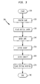
- FIGURE 3 illustrated is an embodiment of a method 300 that is carried out according to the principles of the present invention.
- the method 300 provides a convenient method to assemble an electronic device that combines the favorable heat transfer characteristics of a thermally conductive insert with the heat transfer characteristics of a polymer potting material, which are generally inferior to the thermally conductive inserts.
- the method 300 commences in a "start” step 310.
- a "provide case” step 320 a case that is to at least partially surround the electronic circuit is provided.
- a "place initial layer” step 330 an initial layer of potting material is located within the case.
- the initial layer of potting material has a thickness of about 2 to 6 millimeters.
- the initial layer of potting material is quick-cured (typically by conventional techniques, such as an ultraviolet or microwave process). Of course, other methods of quick-curing the potting material is well within the broad scope of the present invention.
- a "locate insert” step 350 a thermally conductive insert is located within the case.
- the thermally conductive insert may be precut from a sheet of material with a coefficient of thermal conductivity greater than the potting material. Alternatively, the thermally conductive insert may be premolded. In an advantageous embodiment, the thermally conductive insert may be located in the case by a machine, such as a pick and place machine.
- the electronic circuit (having heat generating components thereon) is placed in the case so that the heat-generating components can be located proximate the thermally conductive insert.
- place potting material step 370, polymer potting material with a lower coefficient of thermally conductivity than the thermally conductive insert is placed within the case to encapsulate both the electronic circuit and the insert.
- the method 300 concludes in an send" step 380.
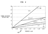
- FIGURE 4 illustrated is a chart plotting thermal resistance per unit area as a function of thickness for combinations of materials having different coefficients of thermal resistance.
- the thermal resistance of regular polymer potting material is indicated by a line 430.
- the result of combining regular potting material with thermally conductive inserts having higher coefficients of thermal conductivity is indicated by respective lines 410, 420.
Landscapes
- Engineering & Computer Science (AREA)
- Microelectronics & Electronic Packaging (AREA)
- Physics & Mathematics (AREA)
- Thermal Sciences (AREA)
- Cooling Or The Like Of Semiconductors Or Solid State Devices (AREA)
- Cooling Or The Like Of Electrical Apparatus (AREA)
- Casings For Electric Apparatus (AREA)
Applications Claiming Priority (2)
| Application Number | Priority Date | Filing Date | Title |
|---|---|---|---|
| US09/496,121 US6317324B1 (en) | 2000-02-01 | 2000-02-01 | Encapsulated power supply with a high thermal conductivity molded insert |
| US496121 | 2000-02-01 |
Publications (2)
| Publication Number | Publication Date |
|---|---|
| EP1122991A2 true EP1122991A2 (de) | 2001-08-08 |
| EP1122991A3 EP1122991A3 (de) | 2003-08-27 |
Family
ID=23971323
Family Applications (1)
| Application Number | Title | Priority Date | Filing Date |
|---|---|---|---|
| EP01300511A Withdrawn EP1122991A3 (de) | 2000-02-01 | 2001-01-22 | Verkapselte elektrische Stromversorgung mit hohe Wärmeleitfähigkeit aufweisendem Einsatz |
Country Status (4)
| Country | Link |
|---|---|
| US (1) | US6317324B1 (de) |
| EP (1) | EP1122991A3 (de) |
| JP (1) | JP2001251076A (de) |
| CN (1) | CN1319889A (de) |
Cited By (4)
| Publication number | Priority date | Publication date | Assignee | Title |
|---|---|---|---|---|
| WO2007061190A1 (en) | 2005-11-22 | 2007-05-31 | Samsung Electronics Co., Ltd. | Method of cooling electronic device and electronic device with improved cooling efficiency |
| DE102007041419A1 (de) * | 2007-08-31 | 2009-03-12 | Sew-Eurodrive Gmbh & Co. Kg | Vorrichtung, insbesondere Elektrogerät, und Verfahren |
| WO2011069533A1 (en) * | 2009-12-07 | 2011-06-16 | Telefonaktiebolaget Lm Ericsson (Publ) | An electronics arrangement |
| FR2956254A1 (fr) * | 2010-02-09 | 2011-08-12 | Peugeot Citroen Automobiles Sa | Connecteur electrique a elements de connexion couples thermiquement par thermo-conduction |
Families Citing this family (33)
| Publication number | Priority date | Publication date | Assignee | Title |
|---|---|---|---|---|
| US6491528B1 (en) * | 1998-12-24 | 2002-12-10 | At&T Wireless Services, Inc. | Method and apparatus for vibration and temperature isolation |
| USD465199S1 (en) | 2002-03-22 | 2002-11-05 | Densei-Lambda Kabushiki Kaisha | Power supply |
| USD464317S1 (en) | 2002-03-22 | 2002-10-15 | Densei-Lambda Kabushiki Kaisha | Power supply |
| US7200011B2 (en) * | 2003-05-02 | 2007-04-03 | Astec International Limited | Thermal interface adapter plate conversion kit and method |
| US7259971B1 (en) * | 2003-08-04 | 2007-08-21 | Z-Axis, Inc. | Encapsulated electronic power converter with embedded AC components |
| US7095615B2 (en) * | 2003-11-13 | 2006-08-22 | Honeywell International, Inc. | Environmentally tuned circuit card assembly and method for manufacturing the same |
| US7576991B2 (en) * | 2004-01-13 | 2009-08-18 | Taisei Plas Co., Ltd. | Electrical equipment for junction and method of manufacturing the same |
| US20050213305A1 (en) * | 2004-03-24 | 2005-09-29 | Patton Electronics, Co. | Integrated internal power supply |
| JP2006203086A (ja) * | 2005-01-24 | 2006-08-03 | Citizen Electronics Co Ltd | 電子部品パッケージ及びその製造方法 |
| US20060286845A1 (en) * | 2005-06-20 | 2006-12-21 | Hinze Lee R | Sealed fastenerless multi-board electronic module and method of manufacture |
| JP2008061399A (ja) * | 2006-08-31 | 2008-03-13 | Mitsumi Electric Co Ltd | Acアダプタ |
| ATE452052T1 (de) * | 2007-05-21 | 2010-01-15 | Magneti Marelli Spa | Elektronische steuereinheit mit erweiterten blöcken |
| US20100202111A1 (en) * | 2007-10-29 | 2010-08-12 | Chien-Kuo Liang | Hermetic modular power supply |
| JP4638923B2 (ja) * | 2008-03-31 | 2011-02-23 | 日立オートモティブシステムズ株式会社 | 制御装置 |
| USD794034S1 (en) * | 2009-01-07 | 2017-08-08 | Samsung Electronics Co., Ltd. | Memory device |
| USD795262S1 (en) * | 2009-01-07 | 2017-08-22 | Samsung Electronics Co., Ltd. | Memory device |
| USD794642S1 (en) * | 2009-01-07 | 2017-08-15 | Samsung Electronics Co., Ltd. | Memory device |
| USD794641S1 (en) * | 2009-01-07 | 2017-08-15 | Samsung Electronics Co., Ltd. | Memory device |
| USD795261S1 (en) * | 2009-01-07 | 2017-08-22 | Samsung Electronics Co., Ltd. | Memory device |
| USD794643S1 (en) * | 2009-01-07 | 2017-08-15 | Samsung Electronics Co., Ltd. | Memory device |
| USD794644S1 (en) * | 2009-01-07 | 2017-08-15 | Samsung Electronics Co., Ltd. | Memory device |
| US8059411B2 (en) * | 2009-07-29 | 2011-11-15 | GM Global Technology Operations LLC | Vehicular electronics assembly |
| JP2012042562A (ja) * | 2010-08-16 | 2012-03-01 | Canon Inc | 撮像装置 |
| US9320131B2 (en) * | 2010-09-17 | 2016-04-19 | Intervention Technology Pty Ltd | Power supply device and components thereof |
| CN102892277B (zh) * | 2011-07-20 | 2016-08-03 | 光宝电子(广州)有限公司 | 电路板装置及其制造方法及具有该电路板装置的电源供应器 |
| AU2011301708B2 (en) * | 2011-09-16 | 2017-03-02 | Intervention Technology Pty Ltd | A power supply device and components thereof |
| US9561604B2 (en) * | 2012-02-28 | 2017-02-07 | Dialight Corporation | Method and apparatus for sky-line potting |
| CN104284559B (zh) * | 2013-07-12 | 2017-09-22 | Tdk株式会社 | 电源装置和电源装置的制造方法 |
| US10244644B2 (en) * | 2015-12-04 | 2019-03-26 | Continental Automotive Systems, Inc. | Automotive electronic device having a cover with fins to reduce gel vibration |
| GB2564188B (en) | 2017-04-24 | 2022-02-09 | Fuji Polymer Ind | Silicone sheet and mounting method using the same |
| JP7415419B2 (ja) * | 2019-10-11 | 2024-01-17 | 株式会社ジェイテクト | 制御装置およびモータ装置 |
| DE102019219230A1 (de) * | 2019-12-10 | 2021-06-10 | Robert Bosch Gmbh | Verfahren zur Ausbildung eines Elektronikmodules |
| DE102024207214A1 (de) * | 2024-07-31 | 2026-02-05 | Brose Fahrzeugteile SE & Co. Kommanditgesellschaft, Würzburg | Elektronik für ein Kraftfahrzeug |
Family Cites Families (5)
| Publication number | Priority date | Publication date | Assignee | Title |
|---|---|---|---|---|
| US3590327A (en) * | 1969-04-24 | 1971-06-29 | Transmation Inc | System for maintaining uniform temperature conditions throughout a body |
| US4029999A (en) * | 1975-04-10 | 1977-06-14 | Ibm Corporation | Thermally conducting elastomeric device |
| US5060113A (en) * | 1987-04-09 | 1991-10-22 | Raychem Corporation | Connector assembly |
| US5381304A (en) * | 1993-06-11 | 1995-01-10 | Honeywell Inc. | Reworkable encapsulated electronic assembly and method of making same |
| EP0926939B1 (de) * | 1997-12-24 | 2003-03-26 | Denso Corporation | Gerät mit Leiterplatte und dessen Zusammenbauverfahren |
-
2000
- 2000-02-01 US US09/496,121 patent/US6317324B1/en not_active Expired - Fee Related
-
2001
- 2001-01-19 CN CN01101668.XA patent/CN1319889A/zh active Pending
- 2001-01-22 EP EP01300511A patent/EP1122991A3/de not_active Withdrawn
- 2001-02-01 JP JP2001025397A patent/JP2001251076A/ja not_active Withdrawn
Cited By (7)
| Publication number | Priority date | Publication date | Assignee | Title |
|---|---|---|---|---|
| WO2007061190A1 (en) | 2005-11-22 | 2007-05-31 | Samsung Electronics Co., Ltd. | Method of cooling electronic device and electronic device with improved cooling efficiency |
| EP1952545A4 (de) * | 2005-11-22 | 2010-10-27 | Samsung Electronics Co Ltd | Verfahren zur kühlung einer elektronischen vorrichtung und elektronische vorrichtung mit erhöhter kühleffizienz |
| EP2747532A1 (de) * | 2005-11-22 | 2014-06-25 | Samsung Electronics Co., Ltd. | Verfahren zur Kühlung einer elektronischen Vorrichtung und elektronische Vorrichtung mit erhöhter Kühleffizienz |
| DE102007041419A1 (de) * | 2007-08-31 | 2009-03-12 | Sew-Eurodrive Gmbh & Co. Kg | Vorrichtung, insbesondere Elektrogerät, und Verfahren |
| DE102007041419B4 (de) | 2007-08-31 | 2022-03-31 | Sew-Eurodrive Gmbh & Co Kg | Anordnung zum Kühlen von elektrischen Bauelementen sowie Umrichter und Kompaktantrieb damit |
| WO2011069533A1 (en) * | 2009-12-07 | 2011-06-16 | Telefonaktiebolaget Lm Ericsson (Publ) | An electronics arrangement |
| FR2956254A1 (fr) * | 2010-02-09 | 2011-08-12 | Peugeot Citroen Automobiles Sa | Connecteur electrique a elements de connexion couples thermiquement par thermo-conduction |
Also Published As
| Publication number | Publication date |
|---|---|
| US6317324B1 (en) | 2001-11-13 |
| EP1122991A3 (de) | 2003-08-27 |
| CN1319889A (zh) | 2001-10-31 |
| JP2001251076A (ja) | 2001-09-14 |
Similar Documents
| Publication | Publication Date | Title |
|---|---|---|
| US6317324B1 (en) | Encapsulated power supply with a high thermal conductivity molded insert | |
| US5910641A (en) | Selectively filled adhesives for compliant, reworkable, and solder-free flip chip interconnection and encapsulation | |
| CA1168764A (en) | Encapsulation for semiconductor integrated circuit chip | |
| EP4207269A1 (de) | Halbleiterverkapselungsstruktur und herstellungsverfahren dafür sowie halbleiterbauelement | |
| JP5384588B2 (ja) | 集積回路製品 | |
| TW529323B (en) | Method for producing electronic device and electronic device and resin filling method | |
| US6445592B1 (en) | Electronic assembly | |
| JPH0754843B2 (ja) | Icチップ用高密度マイクロパッケ−ジ | |
| US8966749B2 (en) | Manufacturing method for protection circuit module of secondary battery | |
| WO1993004498A1 (en) | Lead-on-chip integrated circuit fabrication method and apparatus | |
| US3280378A (en) | Means for anchoring and connecting lead wires in an electrical component | |
| KR100283299B1 (ko) | 플라스틱캡슐화반도체장치및그의제조방법 | |
| JPH05267511A (ja) | 電子装置パッケージおよびその作製方法 | |
| JPH033290A (ja) | 電子回路アセンブリ用サーマルシヤント及びその製造方法 | |
| US6377465B1 (en) | Printing wiring board | |
| US20010045297A1 (en) | Molding of electrical devices with a thermally conductive and electrically insulative polymer composition | |
| JPH08306855A (ja) | 半導体パッケージ、リードフレーム、回路基板、半導体パッケージモールディング用金型及び電子回路盤並にリードフレームの製造方法 | |
| EP0145327B1 (de) | Anordnung einer elektrischen Schnittstelle | |
| CN216413057U (zh) | 半导体电路 | |
| CN114188292A (zh) | 半导体电路和半导体电路的制造方法 | |
| JPH10261847A (ja) | 電子部品搭載用放熱基板 | |
| CN216413050U (zh) | 半导体电路 | |
| US20060163747A1 (en) | Assembly including a circuit and an encapsulation frame, and method of making the same | |
| TW575952B (en) | Lower profile package with power supply in package | |
| CN115279025A (zh) | 电源模块及其制作方法 |
Legal Events
| Date | Code | Title | Description |
|---|---|---|---|
| PUAI | Public reference made under article 153(3) epc to a published international application that has entered the european phase |
Free format text: ORIGINAL CODE: 0009012 |
|
| AK | Designated contracting states |
Kind code of ref document: A2 Designated state(s): AT BE CH CY DE DK ES FI FR GB GR IE IT LI LU MC NL PT SE TR |
|
| AX | Request for extension of the european patent |
Free format text: AL;LT;LV;MK;RO;SI |
|
| PUAL | Search report despatched |
Free format text: ORIGINAL CODE: 0009013 |
|
| AK | Designated contracting states |
Designated state(s): AT BE CH CY DE DK ES FI FR GB GR IE IT LI LU MC NL PT SE TR |
|
| AX | Request for extension of the european patent |
Extension state: AL LT LV MK RO SI |
|
| STAA | Information on the status of an ep patent application or granted ep patent |
Free format text: STATUS: THE APPLICATION IS DEEMED TO BE WITHDRAWN |
|
| 18D | Application deemed to be withdrawn |
Effective date: 20030801 |