EP1122775A2 - Treatment of a metal nitride/metal stack - Google Patents
Treatment of a metal nitride/metal stack Download PDFInfo
- Publication number
- EP1122775A2 EP1122775A2 EP01300928A EP01300928A EP1122775A2 EP 1122775 A2 EP1122775 A2 EP 1122775A2 EP 01300928 A EP01300928 A EP 01300928A EP 01300928 A EP01300928 A EP 01300928A EP 1122775 A2 EP1122775 A2 EP 1122775A2
- Authority
- EP
- European Patent Office
- Prior art keywords
- layer
- nitride layer
- nitride
- nitrogen
- metal
- Prior art date
- Legal status (The legal status is an assumption and is not a legal conclusion. Google has not performed a legal analysis and makes no representation as to the accuracy of the status listed.)
- Withdrawn
Links
Images





Classifications
-
- H—ELECTRICITY
- H10—SEMICONDUCTOR DEVICES; ELECTRIC SOLID-STATE DEVICES NOT OTHERWISE PROVIDED FOR
- H10D—INORGANIC ELECTRIC SEMICONDUCTOR DEVICES
- H10D64/00—Electrodes of devices having potential barriers
- H10D64/01—Manufacture or treatment
- H10D64/011—Manufacture or treatment of electrodes ohmically coupled to a semiconductor
-
- H—ELECTRICITY
- H10—SEMICONDUCTOR DEVICES; ELECTRIC SOLID-STATE DEVICES NOT OTHERWISE PROVIDED FOR
- H10W—GENERIC PACKAGES, INTERCONNECTIONS, CONNECTORS OR OTHER CONSTRUCTIONAL DETAILS OF DEVICES COVERED BY CLASS H10
- H10W20/00—Interconnections in chips, wafers or substrates
- H10W20/01—Manufacture or treatment
- H10W20/031—Manufacture or treatment of conductive parts of the interconnections
- H10W20/032—Manufacture or treatment of conductive parts of the interconnections of conductive barrier, adhesion or liner layers
- H10W20/033—Manufacture or treatment of conductive parts of the interconnections of conductive barrier, adhesion or liner layers in openings in dielectrics
- H10W20/035—Manufacture or treatment of conductive parts of the interconnections of conductive barrier, adhesion or liner layers in openings in dielectrics combinations of barrier, adhesion or liner layers, e.g. multi-layered barrier layers
-
- H—ELECTRICITY
- H10—SEMICONDUCTOR DEVICES; ELECTRIC SOLID-STATE DEVICES NOT OTHERWISE PROVIDED FOR
- H10W—GENERIC PACKAGES, INTERCONNECTIONS, CONNECTORS OR OTHER CONSTRUCTIONAL DETAILS OF DEVICES COVERED BY CLASS H10
- H10W20/00—Interconnections in chips, wafers or substrates
- H10W20/01—Manufacture or treatment
- H10W20/031—Manufacture or treatment of conductive parts of the interconnections
- H10W20/032—Manufacture or treatment of conductive parts of the interconnections of conductive barrier, adhesion or liner layers
- H10W20/047—Manufacture or treatment of conductive parts of the interconnections of conductive barrier, adhesion or liner layers by introducing additional elements therein
- H10W20/048—Manufacture or treatment of conductive parts of the interconnections of conductive barrier, adhesion or liner layers by introducing additional elements therein by using plasmas or gaseous environments, e.g. by nitriding
-
- H—ELECTRICITY
- H10—SEMICONDUCTOR DEVICES; ELECTRIC SOLID-STATE DEVICES NOT OTHERWISE PROVIDED FOR
- H10W—GENERIC PACKAGES, INTERCONNECTIONS, CONNECTORS OR OTHER CONSTRUCTIONAL DETAILS OF DEVICES COVERED BY CLASS H10
- H10W20/00—Interconnections in chips, wafers or substrates
- H10W20/01—Manufacture or treatment
- H10W20/031—Manufacture or treatment of conductive parts of the interconnections
- H10W20/032—Manufacture or treatment of conductive parts of the interconnections of conductive barrier, adhesion or liner layers
- H10W20/052—Manufacture or treatment of conductive parts of the interconnections of conductive barrier, adhesion or liner layers by treatments not introducing additional elements therein
- H10W20/0523—Manufacture or treatment of conductive parts of the interconnections of conductive barrier, adhesion or liner layers by treatments not introducing additional elements therein by irradiating with ultraviolet or particle radiation
Definitions
- the invention relates to a method of processing a substrate for semiconductor device fabrication. More particularly, the invention relates to a method for improving film properties of a metal nitride/metal stack.
- VLSI very large scale integration
- ULSI ultra large scale integration
- W titanium
- Al aluminum
- An integrated barrier/liner structure is typically used to provide good adhesion between the metal conducting layer (W or A1) and the underlying material layer, as well as to prevent undesirable metal diffusion into the underlying layer.
- These barrier/liner structures typically comprise refractory metal nitride/refractory metal combinations - e.g., titanium nitride (TiN)/titanium (Ti), among others.
- Titanium nitride can be deposited by physical vapor deposition (PVD) as well as chemical vapor deposition (CVD).
- CVD TiN may have an amorphous structure - e.g., when deposited from a metallo-organic titanium precursor, as opposed to the more orderly PVD Ti or PVD TiN layers.
- This difference in microstructure results in an integrated CVD TiN/PVD Ti stack having a weaker interfacial link than a PVD TiN/PVD Ti stack.
- structural discontinuity between the TiN and Ti layers also results in high inter-layer stress and interfacial defects.
- Such a barrier/liner structure is often vulnerable to chemical and/or mechanical attack in subsequent processing steps such as W deposition, chemical cleaning and chemical mechanical polishing (CMP).
- subsequently deposited aluminum may also diffuse through defects in the lattice or microstructure of the TiN/Ti stack to react with the underlying materials.
- the present invention is a method of forming a nitride layer on a metal layer, followed by modifying or treating the nitride and at least a portion of the underlying metal layer by exposing the nitride layer to a nitrogen-containing environment.
- Metal nitride/metal stacks formed according to the embodiments of the present invention have improved properties such as enhanced adhesion, reduced interfacial stress and decreased resistivity.
- Such a structure for example, is well-suited for barrier/liner applications in different metallization techniques for sub-0.18 ⁇ m applications.
- the nitrogen-containing environment may comprise gases such as nitrogen (N 2 ) or ammonia (NH 3 ), among others.
- the nitrogen-containing environment may also comprise hydrogen.
- the modification of the metal nitride/metal layers can be performed using plasma or thermal annealing.
- a nitrogen-containing plasma is generated from a gas comprising a mixture of N 2 and hydrogen (H 2 ), or NH 3 .
- the metal layer may comprise a refractory metal such as titanium (Ti), tantalum (Ta), tungsten (W), or combinations thereof, and may be deposited by either physical vapor deposition (PVD) or chemical vapor deposition (CVD).
- the metal nitride layer preferably comprises the same metal as the underlying refractory metal.
- titanium nitride is deposited from a metallo-organic precursor. After TiN deposition, both the TiN layer and the underlying Ti layer are modified by exposing the layer stack to a nitrogen-containing environment for a sufficiently long time to allow active species to penetrate the TiN layer and reach the underlying Ti layer. When the as-deposited TiN layer is treated in an environment comprising both nitrogen and hydrogen, the resulting TiN layer exhibits a reduced impurity content and lower sheet resistance. According to the present invention, a thin nitrated-Ti layer is also formed between the treated TiN and Ti layers. This nitrated-Ti layer provides better lattice matching between the untreated portion of the Ti layer and the treated TiN layer, and leads to an integrated TiN/Ti structure with improved barrier characteristics and reduced inter-layer stress.
- TiN titanium nitride
- a composite metal nitride layer is formed upon a metal layer by repeatedly depositing and treating relatively thin metal nitride layers for additional cycles, until a desired nitride thickness is obtained.
- the entire uppermost nitride layer and a top portion of the underlying material layer are modified, resulting in changes in chemical composition and/or lattice structure. As a result, better lattice matching is obtained across the layer interface, leading to enhanced adhesion and reduced interfacial stress.
- the embodiments of the present invention may further comprise the step of treating the as-deposited metal layer in a first nitrogen-containing environment, prior to the deposition of a metal nitride layer.
- a treatment for example, leads to the formation of a thin nitrated-metal layer, which provides better lattice matching between the untreated portion of the metal layer and the subsequently deposited metal nitride layer.
- the resulting metal nitride/metal stack has enhanced adhesion and reduced stress.
- the as-deposited metal nitride layer is subsequently treated in a second nitrogen-containing environment, which may optionally comprise hydrogen.
- the treatment which is preferably performed in a plasma, modifies both the metal nitride layer and at least a portion of the underlying nitrated-metal layer, resulting in improved film characteristics and interfacial properties.
- the present invention is a method of forming a nitride/metal stack by forming a nitride layer upon a metal layer, followed by treating the nitride layer and a portion of the metal layer in a nitrogen-containing environment.
- this method results in improved interfacial properties of the nitride/metal stack.
- the method can be used, for example, to form a metal nitride/metal stack as a barrier/liner structure in a metallization scheme.
- a refractory metal layer is formed by PVD upon a substrate structure, followed by a deposition of a metal nitride layer by thermal CVD.
- the metal nitride layer is then exposed to a nitrogen-containing environment, during which the entire thickness of the metal nitride layer is treated, resulting in improved physical and chemical characteristics.
- the treatment can either be performed using plasma or thermal annealing, although plasma annealing is generally preferred.
- the treatment step of the present invention is applied for a duration that is sufficient to also partially treat the underlying refractory metal layer, leading to an incorporation of nitrogen (N) into at least a top portion of the underlying metal layer.
- N nitrogen
- the metal nitride deposition and plasma anneal steps are repeated for additional cycles, in order to form a composite metal nitride layer having a desired thickness. Since each of the plasma treatment steps modifies both the top metal nitride layer as well the top portion of the underlying layer, improved interfacial structure can be obtained between each of the component material layers.
- plasma treatment of the PVD metal layer is performed prior to the deposition of a metal nitride layer, resulting in the formation of a thin nitrated-metal layer upon the PVD metal layer.
- a metal nitride layer is deposited upon the nitrated-metal layer, and subjected to plasma treatment according to the present invention.
- the metal nitride layer and a top portion of the underlying nitrated-metal layer are thus modified, and exhibit improved barrier properties and chemical resistance in subsequent processing steps.
- the processes of the present invention can be performed in either a multi-chamber processing apparatus (e.g., a cluster tool) having both PVD and CVD chambers, or separate single-chamber systems.
- a multi-chamber apparatus is preferred because the substrate can be kept within a vacuum environment to prevent contamination between processing steps.
- cluster tools include P5000, Endura and Centura platforms used in conjunction with processing chambers such as a Vectra IMP, Coherent and Standard PVD chamber, a TxZ or a HP TxZ CVD chamber. These cluster tools are commercially available from Applied Materials, Inc., Santa Clara, California.
- FIG. 1 depicts a schematic illustration of a multi-chamber processing apparatus 100, e.g., an Endura system, suitable for performing the CVD and PVD processes of the present invention.
- a multi-chamber processing apparatus 100 e.g., an Endura system
- a similar staged-vacuum wafer processing system is disclosed in United States Patent No. 5,186,718, entitled “Staged-Vacuum Wafer Processing System and Method,” issued to Tepman et al. on February 16, 1993, which is incorporated herein by reference.
- the particular embodiment of the apparatus 100 shown herein is suitable for processing planar substrates, such as semiconductor substrates, and is provided to illustrate the invention, and should not be used to limit the scope of the invention.
- the apparatus 100 typically comprises a cluster of interconnected process chambers, for example, a CVD chamber 102 and a PVD chamber 104.
- a control unit 110 comprises a central processor unit (CPU) 112, support circuitry 114, and memories 116 containing associated control software 118.
- the control unit 112 is used for automated control of the numerous steps required for wafer processing - such as wafer transport, gas flow control, temperature control, chamber evacuation, and so on. Bidirectional communications between the control unit 112 and various components of the apparatus 100 are handled through numerous signal cables collectively referred to as signal buses 120, some of which are illustrated in FIG. 1.
- a computer program code for implementing the processes can be written in any conventional computer readable programming language such as 68000 assembly language, C, C++, or Pascal.
- the program code is then stored or embodied in a computer usable medium.
- FIG. 9 shows an illustrative block diagram of the hierarchical control structure of the control unit 110.
- a user enters a process set and process chamber number into a process selector subroutine 942.
- the process sets are predetermined sets of process parameters or recipes (e.g., gas flow rates, temperature, pressure, ..., etc.) necessary to perform specified processes in a specific process chamber.
- a process sequencer subroutine 943 comprises program code for accepting the identified process chamber and set of process parameters from the process selector subroutine 942, and for controlling operation of the various process chambers.
- the sequencer subroutine 943 includes a program code to perform the steps of (i) monitoring the operation of the process chambers to determine if the chambers are being used, (ii) determining what processes are being performed in the chambers being used, and (iii) executing the desired process based on availability of a process chamber and type of process to be carried out.
- the sequencer subroutine 943 determines which process chamber and process set combination is going to be executed next, the particular process set parameters are passed to the chamber manager subroutines 944a-c which control multiple processing tasks in different process chambers.
- the chamber manager subroutine 944 also controls execution of various chamber component subroutines or program code modules, which control operation of the chamber components necessary to accomplish the selected process set. Examples of chamber component subroutines are substrate positioning subroutine 145, process gas control subroutine 946, pressure control subroutine 947, heater control subroutine 948, and plasma control subroutine 949. Those having ordinary skill in the art would readily recognize that other chamber control subroutines can be included depending on what processes are desired to be performed in the process chamber 102.
- the PVD deposition chamber 104 is used for depositing a metal layer, e.g., titanium (Ti), by sputtering from a metal target inside the chamber 104.
- a metal layer e.g., titanium (Ti)
- Details of a PVD chamber e.g., Model Vectra IMP, have been disclosed in commonly-assigned U.S. patent application, entitled “IMP Technology with Heavy Gas Sputtering", (Docket No. 3495) filed on November 1, 1999, which is herein incorporated by reference.
- an inert gas such as argon (Ar) or xenon (Xe)
- a DC bias current is applied to the sputtering target, with a chamber shield being electrically grounded.
- An RF bias voltage is applied to the substrate support.
- a plasma is generated from the inert gas by applying a DC voltage of about 100-20,000 W, and more typically about 100-10,000 W, to the sputtering target.
- Target materials are sputtered from the target by the plasma, and deposited on the substrate surface.
- the chamber 104 can also be used for plasma treating the deposited metal film.
- a nitrogen-containing plasma may be generated by introducing nitrogen (N 2 ), or other nitrogen-containing gas, into the chamber and applying a RF power of about 10-10000 W, or more typically about 600-2000 W.
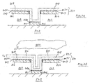
- FIG. 5a-e depict cross-sectional views of a substrate 502 during different stages of integrated circuit device fabrication according to a first embodiment of the invention.
- the substrate 502 refers to any workpiece upon which film processing is performed, and a substrate structure 500 is used to generally denote the substrate 502 together with other material layers formed upon the substrate 502.
- FIG. 5a-e illustrates the formation of a liner/barrier stack inside a contact hole, trench or via structure.
- FIG. 5a shows an insulating layer 503 formed upon an underlying substrate 502, which may comprise aluminum, silicon, tungsten, among others.
- the insulating layer 503 is, for example, a dielectric such as an oxide layer.
- An adhesion or liner layer 506 is then formed upon the insulating layer 503 and the exposed portion 504 of the substrate 502, as shown in FIG. 5b.
- the liner layer 506 comprises a refractory metal - e.g., Ti, Ta, and W, which may be formed using conventional deposition methods such as PVD or CVD.
- a Ti layer 506 may be deposited in a PVD chamber 104 of FIG.
- the metal liner layer 506 may be in the range of about 5 ⁇ to about 1000 ⁇ , and preferably about 100 ⁇ .
- FIG. 5c shows the subsequent formation of a barrier layer 508 upon the metal layer 506, using for example, a CVD technique.
- the barrier layer 508 may comprise a metal nitride such as TiN, tantalum nitride, or tungsten nitride, deposited using appropriate precursors.
- the metal nitride layer 508 comprising TiN may be deposited in either a TxZ or HP TxZ CVD chamber from a TDMAT precursor.
- TiN may also be deposited from a TiCl 4 -based reaction, such as that between TiCl 4 and NH 3 .
- the metal nitride layer 508 is deposited to a thickness d 1 , e.g., in the range of about 5 ⁇ to about 1000 ⁇ , and preferably about 60 ⁇ .
- the as-deposited metal nitride layer 508 is then exposed to a nitrogen-containing plasma 550, as shown in FIG. 5d.
- the plasma 550 may be generated from nitrogen-containing gases, e.g., N 2 or NH 3 , among others.
- Typical process conditions may include a N 2 flow rate in the range of about 100-3000 sccm, preferably about 100-500 sccm, and most preferably about 200-300 sccm; a pressure range of about 1 mtorr-25 torr, preferably about 1-10 torr, and most preferably about 1-6 torr; and a temperature range between room temperature and about 1000°C, preferably about 300-500°C.
- a plasma power of about 10 W to about 10000 W may be used, preferably in the range of about 600-2000 W, and most preferably, about 750 W.
- process conditions may vary for different models of processing chambers used.
- the as-deposited barrier layer 508 is modified by different species in the plasma 550, which may comprise neutral or ionic, atomic or molecular entities. Depending on the specific conditions, the plasma treatment may lead to changes in film density, lattice structure, or film composition. Thus, the thickness d 1t of the treated layer 509 (shown in FIG. 5e) is usually less than the thickness d 1 of the as-deposited layer 508. For example, a 60 ⁇ thick as-deposited TiN layer may be densified to result in a 20 ⁇ thick layer after plasma treatment.
- the present invention treats the entire thickness d 1 of the barrier layer 508 as well as a top portion 506T of the underlying layer 506. This can be accomplished, for example, by using different combinations of process parameters - e.g., an extended plasma treatment time, increased RF power, and so on. After such "over-treatment” (results of which are shown in FIG. 5e), the treated barrier layer 509 becomes more uniform in its film properties, e.g., density, chemical composition, lattice structure, sheet resistance, and so on, compared to a partially-treated layer.
- process parameters e.g., an extended plasma treatment time, increased RF power, and so on.
- the treated barrier layer 509 becomes more uniform in its film properties, e.g., density, chemical composition, lattice structure, sheet resistance, and so on, compared to a partially-treated layer.
- a top or outer portion 506T of the underlying metal layer 506 adjacent to the interface 515 is also modified by the plasma. This occurs when some of the active species from the plasma 550 penetrate the barrier layer 508 to the underlying metal layer 506.
- the sidewall portion of the metal layer 506 can also be treated or modified. Such modifications may include changes in film composition or lattice structure, which may in turn affect film stress, resistivity and density.
- FIG. 5e illustrates that over-treatment by a nitrogen-containing plasma leads to the formation of a thin, "nitrated-metal" layer 507 upon the remaining untreated metal layer 506.
- This may also be referred to as nitration or nitrogen-stuffing - e.g., nitrogen being bonded with Ti or nitrogen atoms being stuffed between Ti grain boundaries.
- nitration or nitrogen-stuffing e.g., nitrogen being bonded with Ti or nitrogen atoms being stuffed between Ti grain boundaries.
- a better atomic lattice structure matching between adjacent layers 506 and 508 reduces inter-layer stress and decreases layering defects or adhesion problems.
- PVD-deposited films e.g., Ti layer 506
- CVD-deposited layers e.g., TiN layer 508 from TDMAT precursor
- this inter-layer stress is further increased due to different thermal expansions of dissimilar material layers.
- film adhesion at the top corners 505C of the via 505 are improved, and the resultant stack 530 is less susceptible to chemical attack during subsequent metal deposition and post-deposition treatment such as chemical mechanical polishing (CMP) and chemical cleaning, and layering defects such as film peeling can be minimized.
- CMP chemical mechanical polishing
- the as-deposited TiN layer may have a microcrystalline structure, instead of being 100% amorphous.
- plasma treatment may also result in enhanced grain growth, and possible changes in crystal orientation.
- the treated nitride layer also exhibits better barrier characteristics due to a reduced sheet resistance and increased film density.
- the nitrogen-containing plasma 550 also comprises hydrogen, such as that generated from a mixture of N 2 and H 2 , or NH 3 .
- hydrogen such as that generated from a mixture of N 2 and H 2 , or NH 3 .
- a plasma for example, is useful for treating a metal nitride layer 508 having some impurity content.
- the as-deposited nitride layer 508 comprises a certain amount of carbon and hydrogen impurities, and is sometimes referred to as a titanium carbo-nitride (TiCN) layer.
- TiCN titanium carbo-nitride
- Hydrogen from the plasma reacts with carbon impurities to form volatile hydrocarbons that desorb from the TiCN layer 508.
- the plasma treatment results in a purified TiN layer 509 with reduced carbon content, as well as increased density due to a modified microstructure. Densification of the TiN layer 509, which depends mostly on the presence of nitrogen in the plasma, also occurs more readily for a more stoichiometric TiN layer.
- an as-deposited TiN layer 508 from a TiCl 4 /NH 3 reaction will also benefit from the presence of hydrogen in the plasma. In that case, the chlorine content in the as-deposited TiN layer 508 can be reduced by reaction with hydrogen, and a decrease in sheet resistance is also obtained.
- N 2 is introduced into the chamber at a flow rate of about 100-3000 sccm, preferably about 100-500 sccm, and most preferably about 200-300 sccm; while H 2 is introduced at a flow rate of about 150-4500 sccm, preferably about 150-750 sccm, and most preferably about 300-450 sccm.
- the chamber pressure is maintained in a range of about 1 mtorr-25 torr, but preferably about 1-10 torr, and most preferably about 1 to about 6 torr.
- the substrate temperature can range from room temperature to about 1000°C, but preferably about 300°C-500°C. However, specific flow rate and pressure conditions may vary for different processing chambers used.
- treatment of the Ti/TiN stack may also be accomplished by thermal annealing at a temperature range of about 350-1100°C for a time duration between about 0.1 minutes to 1500 minutes.
- the effectiveness of the plasma treatment depends on the thickness of the untreated layer, the treatment time and plasma conditions. At a fixed plasma power and treatment time, the thinner the deposited film, the more effective the treatment. For a given film thickness, however, simply increasing the treatment time may not necessarily be the most efficient process choice.
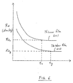
- FIG. 6, shows a plot of the sheet resistance (Rs) vs. plasma treatment time for two different films 601, and 603.
- the sheet resistance of a film depends on both the thickness and the microstructure of the film. For two films having the same thickness, a more ordered microstructure tends to result in a lower sheet resistance; while a thinner film will have a higher sheet resistance than a thicker one if they have similar microstructures.
- Rs decreases with increasing treatment time for two films 601 and 603 having similar microstructures but different thicknesses, x and y, where x is less than y.
- a treatment time t y is required for the film to reach saturation - i.e., its sheet resistance approaches a limiting value of Rs y , and increasing the treatment time beyond t y will not result in further decrease of its sheet resistance.
- the treatment time t x required to thoroughly treat a thinner film 601 (thickness x) - i.e., to reach its limiting sheet resistance RS x is shorter than t y .
- the present invention provides a method by which a thicker film 603 can be formed more efficiently by repeating the deposition and treatment steps for additional cycles.
- the thinner component film 601 is first deposited and plasma treated according to the present invention.
- a second, relatively thin, component TiN film is deposited upon the treated film 601 to form a composite film.
- Thorough plasma treatment of the second component film can be accomplished in a relatively short time.
- a composite film of a final desired thickness may be fabricated with favorable film characteristics that are otherwise not readily achievable by using a single-step deposition and treatment procedure.
- FIGS. 7a-d depict such an alternative embodiment, in which a composite barrier layer is formed by repeating the deposition and plasma treatment steps for additional cycles.
- FIG. 7a illustrates the cross-sectional view of a substrate structure 700 after the first plasma treatment previously described.
- a second barrier layer 708 comprising metal nitride is then deposited upon the treated layer 509, to a thickness d 2 of about 5-1000 ⁇ , preferably 60 ⁇ , as shown in FIG. 7b.
- the layer 708 may be deposited under process conditions that are different from those used for the layer 508, it is typical that the same process conditions be used.
- the as-deposited layer 708 is then exposed to a nitrogen-containing plasma 750, as shown in FIG. 7c.
- the second plasma treatment is performed for a sufficiently long time to ensure thorough treatment of the entire thickness d 2 of the second barrier layer. 708, and at least a top portion 509T of the first barrier layer 509.
- FIG. 7d illustrates the treated barrier layer 709, which may be modified in chemical composition and/or lattice structure compared to the as-deposited layer 708.
- the top portion 509T of the first barrier layer 509 is further modified during the second treatment, and may be denoted as an interface layer 710. As such, structural continuity between the first barrier layer 509 and the second barrier layer 709 is improved.
- the composite barrier layer 720 comprising the treated barrier layers 709 and 509, has a thickness d f , which is typically less than the sum of d 1 and d 2 because of film densification by plasma treatment. Further processing steps such as deposition, lithography, etching, implant, and the like, are then performed as appropriate to complete the fabrication of the IC device.
- FIGS. 8a-f illustrate yet another embodiment of the invention, in which a metal layer 806 is plasma treated prior to metal nitride deposition.
- FIG. 8a shows the metal layer 806 which has been deposited upon a substrate structure 500 such as that depicted in FIG. 5a.
- the metal layer 806, e.g., Ti, Ta or W may be deposited from sputtering a metal target in a PVD chamber, or may also be formed by a CVD technique.
- FIG. 8b illustrates the as-deposited metal layer 806 being exposed to a nitrogen-containing plasma 850, which may comprise a variety of gases, such as N 2 or NH 3 , among others.
- a thin metal nitride layer 807 (or nitrated-metal layer) is formed after this plasma step, as shown in FIG. 8c.
- the plasma treatment of the metal layer 806 can be performed in the same chamber used for the deposition of the metal layer 806. Although a plasma is the preferred method of film treatment or annealing, thermal annealing may also be used to facilitate nitration of the metal layer 806.
- plasma treatment of the metal layer 806 may be performed in the chamber used for subsequent metal nitride deposition.
- an additional benefit can be realized - that of substrate pre-conditioning.
- film deposition processes are temperature dependent, and a single-wafer processing chamber may exhibit a "first wafer" effect. That is, the temperature in the chamber may not be stabilized when the first wafer in a batch is being processed. As such, the film deposited on the first wafer may have a slightly different thickness, or uniformity, compared to subsequently processed wafers.
- each wafer in the batch, including the first wafer is heated to about the same temperature by the treating plasma prior to nitride deposition.
- Such wafer pre-conditioning is effective in improving wafer-to-wafer reproducibility in the deposited metal nitride film.
- FIG. 8c illustrates a metal nitride layer 808, preferably comprising the same refractory metal as the metal layer 806, being deposited to a thickness t 1 upon the nitrated-metal layer 807.
- the thickness t 1 may be in the range of about 5-1000 ⁇ , and preferably about 60 ⁇ .
- the nitrated-metal layer 807 serves as an interfacial link, and provides an improved lattice matching between the untreated metal layer 806 and the nitride layer 808.
- the TiN layer 808 may also be "seeded" by the nitrated-metal layer 807. That is, the nitride layer 808 may have a preferred crystal orientation similar to that of the nitrated-metal layer 807.
- FIG. 8d illustrates the as-deposited metal nitride layer 808 being subjected to a plasma treatment step according to the present invention.
- the plasma 852 may be a nitrogen-containing plasma, comprising for example, N 2 or NH 3 .
- the entire metal nitride layer 808 and at least a top portion 807T of the underlying nitrated-metal interfacial layer 807 are treated such that they are modified in terms of lattice structure and/or chemical composition.
- Enhanced lattice structure matching from the plasma treatment results in a metal nitride/metal stack 830 (shown in FIG.
- the modified nitride layer 809 comprising the modified nitride layer 809, the treated nitrated-metal portion 807T, the nitrated-metal layer 807, and the untreated metal layer 806) with improved barrier/liner characteristics.
- the treated nitride layer 809 has a thickness that is less than t 1 .
- the plasma treatment step may also be performed to further treat a portion of the underlying metal layer 806 (adjacent to the nitrated-metal layer 807), e.g., by extending the treatment time and/or modifying the plasma conditions.
- the nitride/metal stack 830 may be used as a barrier/liner in a metallization scheme.
- the nitride deposition and treatment steps may be repeated for additional cycles. This is illustrated in FIG. 8f, in which a second nitride layer 810 is deposited to a thickness t 2 in the range of about 5-1000 ⁇ , preferably about 60 ⁇ , upon the metal stack 830.
- the as-deposited nitride layer 810 is then exposed to a nitrogen-containing plasma 854, which may or may not be identical to plasma 852.
- the plasma 854 is used to treat the entire second nitride layer 810 and a top portion of the underlying nitride layer 809.
- the primary purpose of this treatment step is to provide an improved interface 825 between the second nitride layer 810 and the first nitride layer 809. Additional nitride layers may be deposited and plasma treated to yield a composite nitride layer of desired final thickness.
- NxD a process comprising the formation of a composite layer by repeated deposition and treatment of component layers
- NxD the number of deposition-treatment cycles
- D the thickness of the plasma-treated component layer
- a composite TiN film or layer having a thickness of about 40 ⁇ is formed upon an underlying Ti layer in a "2x20" process performed in a HP TxZ chamber.
- This process involves two cycles of forming 20 ⁇ thick TiN. Each cycle comprises two steps: first, depositing a film comprising TiN of about 60 ⁇ ; and second, exposing the deposited film to a plasma environment comprising N 2 and hydrogen (H 2 ).
- the plasma treatment results in a densified film having a typical thickness of about 20 ⁇ , and a sheet resistance of about 1500 ohm/sq. Similar to other embodiments previously described, this embodiment is generally applicable to contact and via levels.
- Table 1 illustrates several key steps in a typical 2x20 process recipe for the treatment and deposition of TiN.
- Recipe for TiN "2x20" Process #1 Dep1 #2 Pls1 #3 Cooldown #4 Dep2 #5 Pls2 Inert Dil.
- (sccm) 1300 - 1900 1300 - He Car.
- a wafer e.g., one having a previously deposited adhesion layer
- backside pressure control is enabled such that a pressure difference of about 1.5 torr is maintained between the front and the backside of the wafer throughout the entire process recipe.
- the heater temperature is typically set at about 365°C, with the edge purge and bottom purge gas flows at about 1500 sccm and 1000 sccm, respectively.
- Inert dilutant and carrier gas flows are also established prior to the deposition of the first barrier layer, which is shown in step #1.
- Gases such as N 2 , Ar, He and H 2 , among others, are suitable for use as dilutant gases, and a total flow rate of about 1300 sccm may be used.
- TDMAT is introduced into the chamber by passing a He carrier gas through a bubbler or ampoule containing TDMAT at a temperature of about 50°C. Alternatively, liquid injection of TDMAT may also be used.
- a TiN layer of about 60 ⁇ , for example, is deposited upon the wafer after step #1.
- Plasma treatment of the as-deposited TiN layer is performed in step #2, using N 2 and H 2 precursors at flow rates of about 300 sccm and 450 sccm, respectively.
- the chamber pressure is maintained at about 1.3 torr, while an RF power of about 750 W is applied to the showerhead.
- a final TiN layer of about 20 ⁇ is obtained.
- the wafer, which is heated up during the plasma treatment step, is allowed to cool down in step #3, during which no TDMAT is supplied to the chamber.
- a second TiN layer is subsequently deposited in step #4, preferably under the same conditions as that of step #1, followed by a second plasma treatment step #5.
- a TiN layer having a final thickness of about 40 ⁇ is formed upon the wafer, and the chamber is purged with an inert gas, e.g., N 2 , prior to the removal of the wafer.
- the various embodiments of the present invention are generally applicable to forming metal nitride/metal stacks in CVD W, Al and Cu metallization schemes, as well as to any contact and via levels.
- the metal layer may be formed by conventional means known in the art over a variety of different substrates including silicon, thermal oxides and ceramics, among others.
- the process of the present invention can be performed over a variety of patterned wafers having different combinations of underlying and interconnecting layers of various materials.
Landscapes
- Electrodes Of Semiconductors (AREA)
- Chemical Vapour Deposition (AREA)
- Internal Circuitry In Semiconductor Integrated Circuit Devices (AREA)
- Physical Vapour Deposition (AREA)
Abstract
Description
| Recipe for TiN "2x20" | |||||
| # | |||||
| 1 Dep1 | #2 Pls1 | #3 Cooldown | #4 Dep2 | #5 Pls2 | |
| Inert Dil. (sccm) | 1300 | - | 1900 | 1300 | - |
| He Car. (sccm) | 325 | - | 325 | 325 | - |
| TDMAT | No TDMAT | TDMAT | |||
| N2 (sccm) | 300 | 300 | |||
| H2 (sccm) | 450 | 450 | |||
| Pressure (torr) | 5.0 | 1.3 | 5.0 | 5.0 | 1.3 |
| RF Power (W) | 0 | 750 | 0 | 0 | 750 |
| Time (sec) | 18 | 20 | 5 | 18 | 20 |
Claims (27)
- A method of processing a substrate, the method comprising the steps of:(a) depositing a nitride layer upon a metal layer to form an interface between said nitride layer and said metal layer;(b) providing a nitrogen-containing environment; and(c) modifying said nitride layer and at least a portion of said metal layer below said interface by exposing said nitride layer to said nitrogen-containing environment.
- The method of claim 1, wherein said step (c) comprises adding nitrogen to said portion of said metal layer below said interface.
- The method of claim 1 or claim 2, wherein said step (c) comprises reducing microstructure mismatch across said interface formed in said step (a).
- The method of any one of claims 1 to 3, wherein said nitride layer of said step (a) further comprises carbon and/or chlorine, and said nitrogen-containing environment in said step (c) further comprises hydrogen.
- The method of claim 4, wherein said step (c) comprises reducing carbon and/or chlorine from said nitride layer and changing the microstructure of said portion of said metal layer below said interface.
- The method of an one of claims 1 to 5, further comprising the steps of:(d) after step (c), depositing a nitride layer upon said modified nitride layer to form a nitride-nitride interface;(e) modifying said deposited nitride layer of step (d) and at least a portion of said modified nitride layer from step (c) by exposing said deposited nitride layer to a nitrogen-containing environment.
- A method of processing a substrate, the method comprising the steps of:(a) depositing a nitride layer upon a metal layer to form an interface between said nitride layer and said metal layer;(b) providing a nitrogen-containing plasma; and(c) modifying said nitride layer and at least a portion of said metal layer below said interface by exposing said nitride layer to said nitrogen-containing plasma.
- The method of claim 7, wherein said nitride layer of said step (a) further comprises carbon or chlorine, and said nitrogen-containing plasma in said step (c) further comprises hydrogen.
- The method of any one of claims 1 to 8, wherein said step (a) is performed in the presence of a metallo-organic compound comprising titanium.
- The method of claim 9, wherein said metallo-organic compound is tetrakis-dimethylamino-titanium (TDMAT).
- The method of any one of claims 7 to 10, further comprising the steps of:(d) after step (c), depositing a nitride layer upon said modified nitride layer to form a nitride-nitride interface; and(e) modifying said deposited nitride layer of step (d) and at least a portion of said modified nitride layer from step (c) by exposing said deposited nitride layer to a nitrogen-containing plasma.
- The method of claim 6 or claim 11, wherein said modifying step (e) comprises reducing microstructure mismatch across said nitride-nitride interface of step (d).
- A method for processing a substrate, the method comprising the steps of:(a) depositing a first nitride layer upon a metal layer to form a first interface between said first nitride layer and said metal layer;(b) providing a first nitrogen-containing environment;(c) modifying said first nitride layer of step (a) and at least a portion of said metal layer of step (a) by exposing said first nitride layer to said first nitrogen-containing environment, wherein nitrogen is added to said portion of said metal layer in the vicinity of said first interface;(d) depositing a second nitride layer upon said first nitride layer after said modifying step (c) to form a second interface between said first nitride layer and said second nitride layer;(e) providing a second nitrogen-containing environment; and(f) modifying said second nitride layer and at least a portion of said first nitride layer in the vicinity of said second interface by exposing said second nitride layer to said second nitrogen-containing environment.
- The method of claim 13, wherein said modifying step (c) comprises reducing microstructure mismatch across said first interface between said metal layer and first nitride layer.
- The method of claim 13 or claim 14, wherein said first nitride layer of said step (a) further comprises carbon or chlorine and said modifying step (c) comprises reducing carbon or chlorine from said first nitride layer.
- The method of any one of claims 13 to 15, wherein said first nitrogen-containing environment and said second nitrogen-containing environment further comprise hydrogen.
- The method of any one of claim 13 to 16, wherein said modifying step (f) comprises reducing microstructure mismatch across said second interface formed between said first nitride layer and said second nitride layer.
- The method of any one of claims 13 to 17, wherein said first nitrogen-containing environment is a first plasma and said second nitrogen-containing environment is a second plasma.
- A method for processing a substrate, the method comprising the steps of:(a) forming a metal layer upon a substrate;(b) exposing said metal layer to a first nitrogen-containing environment to form a nitrated-metal layer from at least a top portion of said metal layer;(c) depositing a nitride layer upon said nitrated-metal layer to form an interface between said nitride layer and said nitrated-metal layer; and(d) modifying said nitride layer and at least a portion of said nitrated-metal layer adjacent said first interface by exposing said nitride layer of said step (c) to a second nitrogen-containing environment.
- The method of claim 19, further comprising the steps of:(e) after step (d), depositing a nitride layer upon said plasma-modified nitride layer to form a nitride-nitride interface;(f) forming a nitrogen-containing plasma; and(g) modifying said nitride-nitride interface by exposing said deposited nitride layer of step (e) to said nitrogen-containing plasma of step (f).
- The method of claim 20, wherein said modifying step (g) comprises reducing microstructure mismatch across said nitride-nitride interface.
- The method of any one of claims 1 to 21, wherein said metal layer comprises or consists of one or more of titanium (Ti), tantalum (Ta) and tungsten (W) and said nitride layer comprises or consists of one or more of titanium nitride, tantalum nitride and tungsten nitride.
- A computer readable medium containing a software routine that, when executed, causes a general purpose computer to control a substrate processing chamber using a method comprising the steps of:(a) forming a metal layer upon a substrate;(b) depositing a nitride layer upon said metal layer to form an interface between said nitride layer and said metal layer;(c) providing a nitrogen-containing environment; and(d) modifying said nitride layer and at least a portion of said metal layer below said interface by exposing said nitride layer to said nitrogen-containing environment.
- The computer readable medium of claim 23, wherein said modifying step (d) of said method comprises adding nitrogen to said portion of said metal layer below said interface.
- The computer readable medium of claim 23 or claim 24, wherein said modifying step (d) of said method comprises reducing microstructure mismatch across said interface of step (b).
- A computer program product, which when read by a computer causes the said computer to control a substrate processing chamber using a method comprising the steps of:(a) forming a metal layer upon a substrate;(b) depositing a nitride layer upon said metal layer to form an interface between said nitride layer and said metal layer;(c) providing a nitrogen-containing environment; and(d) modifying said nitride layer and at least a portion of said metal layer below said interface by exposing said nitride layer to said nitrogen-containing environment.
- A storage medium upon which is stored a computer program product as defined in claim 26.
Applications Claiming Priority (2)
| Application Number | Priority Date | Filing Date | Title |
|---|---|---|---|
| US495817 | 1995-06-27 | ||
| US09/495,817 US6436819B1 (en) | 2000-02-01 | 2000-02-01 | Nitrogen treatment of a metal nitride/metal stack |
Publications (2)
| Publication Number | Publication Date |
|---|---|
| EP1122775A2 true EP1122775A2 (en) | 2001-08-08 |
| EP1122775A3 EP1122775A3 (en) | 2001-08-16 |
Family
ID=23970101
Family Applications (1)
| Application Number | Title | Priority Date | Filing Date |
|---|---|---|---|
| EP01300928A Withdrawn EP1122775A3 (en) | 2000-02-01 | 2001-02-01 | Treatment of a metal nitride/metal stack |
Country Status (5)
| Country | Link |
|---|---|
| US (1) | US6436819B1 (en) |
| EP (1) | EP1122775A3 (en) |
| JP (1) | JP4947840B2 (en) |
| KR (1) | KR100748371B1 (en) |
| SG (1) | SG94727A1 (en) |
Families Citing this family (444)
| Publication number | Priority date | Publication date | Assignee | Title |
|---|---|---|---|---|
| US6734110B1 (en) * | 1999-10-14 | 2004-05-11 | Taiwan Semiconductor Manufacturing Company | Damascene method employing composite etch stop layer |
| US6689220B1 (en) * | 2000-11-22 | 2004-02-10 | Simplus Systems Corporation | Plasma enhanced pulsed layer deposition |
| US20020106881A1 (en) * | 2000-12-07 | 2002-08-08 | Jain Manoj K. | Prevention of contact failure by hydrogen treatment |
| JP2002217292A (en) * | 2001-01-23 | 2002-08-02 | Hitachi Ltd | Semiconductor integrated circuit device and method of manufacturing semiconductor integrated circuit device |
| US6951804B2 (en) | 2001-02-02 | 2005-10-04 | Applied Materials, Inc. | Formation of a tantalum-nitride layer |
| US9708707B2 (en) * | 2001-09-10 | 2017-07-18 | Asm International N.V. | Nanolayer deposition using bias power treatment |
| US6500761B1 (en) * | 2001-10-24 | 2002-12-31 | Tokyo Electron Limited | Method for improving the adhesion and durability of CVD tantalum and tantalum nitride modulated films by plasma treatment |
| US6866255B2 (en) * | 2002-04-12 | 2005-03-15 | Xerox Corporation | Sputtered spring films with low stress anisotropy |
| US6583507B1 (en) * | 2002-04-26 | 2003-06-24 | Bum Ki Moon | Barrier for capacitor over plug structures |
| US7163721B2 (en) * | 2003-02-04 | 2007-01-16 | Tegal Corporation | Method to plasma deposit on organic polymer dielectric film |
| US9121098B2 (en) | 2003-02-04 | 2015-09-01 | Asm International N.V. | NanoLayer Deposition process for composite films |
| US7713592B2 (en) * | 2003-02-04 | 2010-05-11 | Tegal Corporation | Nanolayer deposition process |
| US20040175926A1 (en) * | 2003-03-07 | 2004-09-09 | Advanced Micro Devices, Inc. | Method for manufacturing a semiconductor component having a barrier-lined opening |
| JP2004311545A (en) * | 2003-04-03 | 2004-11-04 | Matsushita Electric Ind Co Ltd | Semiconductor device manufacturing method and high melting point metal film deposition apparatus |
| US20050112876A1 (en) * | 2003-11-26 | 2005-05-26 | Chih-Ta Wu | Method to form a robust TiCI4 based CVD TiN film |
| US20050133165A1 (en) * | 2003-12-23 | 2005-06-23 | Taiwan Semiconductor Manufacturing Co. | Apparatus for the prevention of arcing in a CVD-TiN chamber |
| KR100597649B1 (en) | 2004-11-26 | 2006-07-05 | 삼성전자주식회사 | Method for fabricating semiconductor device comprising barrier metal and its structure |
| KR100645207B1 (en) * | 2005-02-23 | 2006-11-10 | 주식회사 하이닉스반도체 | Wiring Formation Method of Semiconductor Device |
| US8039391B1 (en) * | 2006-03-27 | 2011-10-18 | Spansion Llc | Method of forming a contact in a semiconductor device with engineered plasma treatment profile of barrier metal layer |
| KR101262432B1 (en) * | 2006-03-30 | 2013-05-08 | 후지쯔 세미컨덕터 가부시키가이샤 | Method for manufacturing semiconductor device |
| US7575638B2 (en) * | 2007-02-02 | 2009-08-18 | Lam Research Corporation | Apparatus for defining regions of process exclusion and process performance in a process chamber |
| TW200814156A (en) * | 2006-07-21 | 2008-03-16 | Toshiba Kk | Method for manufacturing semiconductor device and semiconductor device |
| US7772014B2 (en) * | 2007-08-28 | 2010-08-10 | Texas Instruments Incorporated | Semiconductor device having reduced single bit fails and a method of manufacture thereof |
| JP4331791B2 (en) * | 2007-10-09 | 2009-09-16 | パナソニック株式会社 | Film forming method and film forming apparatus |
| US10378106B2 (en) | 2008-11-14 | 2019-08-13 | Asm Ip Holding B.V. | Method of forming insulation film by modified PEALD |
| US9394608B2 (en) | 2009-04-06 | 2016-07-19 | Asm America, Inc. | Semiconductor processing reactor and components thereof |
| US8802201B2 (en) | 2009-08-14 | 2014-08-12 | Asm America, Inc. | Systems and methods for thin-film deposition of metal oxides using excited nitrogen-oxygen species |
| US8278139B2 (en) * | 2009-09-25 | 2012-10-02 | Applied Materials, Inc. | Passivating glue layer to improve amorphous carbon to metal adhesion |
| JP5375497B2 (en) * | 2009-10-01 | 2013-12-25 | トヨタ自動車株式会社 | Semiconductor device and method for manufacturing semiconductor device |
| KR101725152B1 (en) * | 2010-11-11 | 2017-04-11 | 에스케이하이닉스 주식회사 | Manufacturing Method Of Metal line of Semiconductor Device |
| KR20120122548A (en) * | 2011-04-29 | 2012-11-07 | 에스케이하이닉스 주식회사 | Semiconductor device and method for fabricating the same |
| US9136180B2 (en) | 2011-06-01 | 2015-09-15 | Asm Ip Holding B.V. | Process for depositing electrode with high effective work function |
| US9312155B2 (en) | 2011-06-06 | 2016-04-12 | Asm Japan K.K. | High-throughput semiconductor-processing apparatus equipped with multiple dual-chamber modules |
| US9793148B2 (en) | 2011-06-22 | 2017-10-17 | Asm Japan K.K. | Method for positioning wafers in multiple wafer transport |
| US10364496B2 (en) | 2011-06-27 | 2019-07-30 | Asm Ip Holding B.V. | Dual section module having shared and unshared mass flow controllers |
| US10854498B2 (en) | 2011-07-15 | 2020-12-01 | Asm Ip Holding B.V. | Wafer-supporting device and method for producing same |
| US20130023129A1 (en) | 2011-07-20 | 2013-01-24 | Asm America, Inc. | Pressure transmitter for a semiconductor processing environment |
| US9017481B1 (en) | 2011-10-28 | 2015-04-28 | Asm America, Inc. | Process feed management for semiconductor substrate processing |
| WO2013063260A1 (en) * | 2011-10-28 | 2013-05-02 | Applied Materials, Inc. | High temperature tungsten metallization process |
| JP5651616B2 (en) * | 2012-02-17 | 2015-01-14 | 株式会社東芝 | Magnetic recording medium and manufacturing method thereof |
| US8946830B2 (en) | 2012-04-04 | 2015-02-03 | Asm Ip Holdings B.V. | Metal oxide protective layer for a semiconductor device |
| US9558931B2 (en) | 2012-07-27 | 2017-01-31 | Asm Ip Holding B.V. | System and method for gas-phase sulfur passivation of a semiconductor surface |
| US9659799B2 (en) | 2012-08-28 | 2017-05-23 | Asm Ip Holding B.V. | Systems and methods for dynamic semiconductor process scheduling |
| US9021985B2 (en) | 2012-09-12 | 2015-05-05 | Asm Ip Holdings B.V. | Process gas management for an inductively-coupled plasma deposition reactor |
| US9324811B2 (en) | 2012-09-26 | 2016-04-26 | Asm Ip Holding B.V. | Structures and devices including a tensile-stressed silicon arsenic layer and methods of forming same |
| US10714315B2 (en) | 2012-10-12 | 2020-07-14 | Asm Ip Holdings B.V. | Semiconductor reaction chamber showerhead |
| US9640416B2 (en) | 2012-12-26 | 2017-05-02 | Asm Ip Holding B.V. | Single-and dual-chamber module-attachable wafer-handling chamber |
| US20160376700A1 (en) | 2013-02-01 | 2016-12-29 | Asm Ip Holding B.V. | System for treatment of deposition reactor |
| US9589770B2 (en) | 2013-03-08 | 2017-03-07 | Asm Ip Holding B.V. | Method and systems for in-situ formation of intermediate reactive species |
| US9484191B2 (en) | 2013-03-08 | 2016-11-01 | Asm Ip Holding B.V. | Pulsed remote plasma method and system |
| US8993054B2 (en) | 2013-07-12 | 2015-03-31 | Asm Ip Holding B.V. | Method and system to reduce outgassing in a reaction chamber |
| US9018111B2 (en) | 2013-07-22 | 2015-04-28 | Asm Ip Holding B.V. | Semiconductor reaction chamber with plasma capabilities |
| US9793115B2 (en) | 2013-08-14 | 2017-10-17 | Asm Ip Holding B.V. | Structures and devices including germanium-tin films and methods of forming same |
| US9240412B2 (en) | 2013-09-27 | 2016-01-19 | Asm Ip Holding B.V. | Semiconductor structure and device and methods of forming same using selective epitaxial process |
| US9556516B2 (en) | 2013-10-09 | 2017-01-31 | ASM IP Holding B.V | Method for forming Ti-containing film by PEALD using TDMAT or TDEAT |
| US10179947B2 (en) | 2013-11-26 | 2019-01-15 | Asm Ip Holding B.V. | Method for forming conformal nitrided, oxidized, or carbonized dielectric film by atomic layer deposition |
| US10683571B2 (en) | 2014-02-25 | 2020-06-16 | Asm Ip Holding B.V. | Gas supply manifold and method of supplying gases to chamber using same |
| US10167557B2 (en) | 2014-03-18 | 2019-01-01 | Asm Ip Holding B.V. | Gas distribution system, reactor including the system, and methods of using the same |
| US9447498B2 (en) | 2014-03-18 | 2016-09-20 | Asm Ip Holding B.V. | Method for performing uniform processing in gas system-sharing multiple reaction chambers |
| US11015245B2 (en) | 2014-03-19 | 2021-05-25 | Asm Ip Holding B.V. | Gas-phase reactor and system having exhaust plenum and components thereof |
| US9404587B2 (en) | 2014-04-24 | 2016-08-02 | ASM IP Holding B.V | Lockout tagout for semiconductor vacuum valve |
| US10858737B2 (en) | 2014-07-28 | 2020-12-08 | Asm Ip Holding B.V. | Showerhead assembly and components thereof |
| US9543180B2 (en) | 2014-08-01 | 2017-01-10 | Asm Ip Holding B.V. | Apparatus and method for transporting wafers between wafer carrier and process tool under vacuum |
| US9890456B2 (en) | 2014-08-21 | 2018-02-13 | Asm Ip Holding B.V. | Method and system for in situ formation of gas-phase compounds |
| US9657845B2 (en) | 2014-10-07 | 2017-05-23 | Asm Ip Holding B.V. | Variable conductance gas distribution apparatus and method |
| US10941490B2 (en) | 2014-10-07 | 2021-03-09 | Asm Ip Holding B.V. | Multiple temperature range susceptor, assembly, reactor and system including the susceptor, and methods of using the same |
| KR102300403B1 (en) | 2014-11-19 | 2021-09-09 | 에이에스엠 아이피 홀딩 비.브이. | Method of depositing thin film |
| KR102263121B1 (en) | 2014-12-22 | 2021-06-09 | 에이에스엠 아이피 홀딩 비.브이. | Semiconductor device and manufacuring method thereof |
| US9478415B2 (en) | 2015-02-13 | 2016-10-25 | Asm Ip Holding B.V. | Method for forming film having low resistance and shallow junction depth |
| US10529542B2 (en) | 2015-03-11 | 2020-01-07 | Asm Ip Holdings B.V. | Cross-flow reactor and method |
| US10276355B2 (en) | 2015-03-12 | 2019-04-30 | Asm Ip Holding B.V. | Multi-zone reactor, system including the reactor, and method of using the same |
| US10458018B2 (en) | 2015-06-26 | 2019-10-29 | Asm Ip Holding B.V. | Structures including metal carbide material, devices including the structures, and methods of forming same |
| US10600673B2 (en) | 2015-07-07 | 2020-03-24 | Asm Ip Holding B.V. | Magnetic susceptor to baseplate seal |
| US10043661B2 (en) | 2015-07-13 | 2018-08-07 | Asm Ip Holding B.V. | Method for protecting layer by forming hydrocarbon-based extremely thin film |
| US9899291B2 (en) | 2015-07-13 | 2018-02-20 | Asm Ip Holding B.V. | Method for protecting layer by forming hydrocarbon-based extremely thin film |
| US9472502B1 (en) | 2015-07-14 | 2016-10-18 | Taiwan Semiconductor Manufacturing Co., Ltd. | Cobalt interconnect techniques |
| US10083836B2 (en) | 2015-07-24 | 2018-09-25 | Asm Ip Holding B.V. | Formation of boron-doped titanium metal films with high work function |
| US10087525B2 (en) | 2015-08-04 | 2018-10-02 | Asm Ip Holding B.V. | Variable gap hard stop design |
| US9647114B2 (en) | 2015-08-14 | 2017-05-09 | Asm Ip Holding B.V. | Methods of forming highly p-type doped germanium tin films and structures and devices including the films |
| US9711345B2 (en) | 2015-08-25 | 2017-07-18 | Asm Ip Holding B.V. | Method for forming aluminum nitride-based film by PEALD |
| US9960072B2 (en) | 2015-09-29 | 2018-05-01 | Asm Ip Holding B.V. | Variable adjustment for precise matching of multiple chamber cavity housings |
| US9909214B2 (en) | 2015-10-15 | 2018-03-06 | Asm Ip Holding B.V. | Method for depositing dielectric film in trenches by PEALD |
| US10211308B2 (en) | 2015-10-21 | 2019-02-19 | Asm Ip Holding B.V. | NbMC layers |
| US10322384B2 (en) | 2015-11-09 | 2019-06-18 | Asm Ip Holding B.V. | Counter flow mixer for process chamber |
| US9455138B1 (en) | 2015-11-10 | 2016-09-27 | Asm Ip Holding B.V. | Method for forming dielectric film in trenches by PEALD using H-containing gas |
| US10134801B2 (en) | 2015-11-30 | 2018-11-20 | Taiwan Semiconductor Manufacturing Company Limited | Method of forming deep trench isolation in radiation sensing substrate and image sensor device |
| US9905420B2 (en) | 2015-12-01 | 2018-02-27 | Asm Ip Holding B.V. | Methods of forming silicon germanium tin films and structures and devices including the films |
| US9607837B1 (en) | 2015-12-21 | 2017-03-28 | Asm Ip Holding B.V. | Method for forming silicon oxide cap layer for solid state diffusion process |
| US9735024B2 (en) | 2015-12-28 | 2017-08-15 | Asm Ip Holding B.V. | Method of atomic layer etching using functional group-containing fluorocarbon |
| US9627221B1 (en) | 2015-12-28 | 2017-04-18 | Asm Ip Holding B.V. | Continuous process incorporating atomic layer etching |
| US11139308B2 (en) | 2015-12-29 | 2021-10-05 | Asm Ip Holding B.V. | Atomic layer deposition of III-V compounds to form V-NAND devices |
| US10468251B2 (en) | 2016-02-19 | 2019-11-05 | Asm Ip Holding B.V. | Method for forming spacers using silicon nitride film for spacer-defined multiple patterning |
| US10529554B2 (en) | 2016-02-19 | 2020-01-07 | Asm Ip Holding B.V. | Method for forming silicon nitride film selectively on sidewalls or flat surfaces of trenches |
| US9754779B1 (en) | 2016-02-19 | 2017-09-05 | Asm Ip Holding B.V. | Method for forming silicon nitride film selectively on sidewalls or flat surfaces of trenches |
| US10501866B2 (en) | 2016-03-09 | 2019-12-10 | Asm Ip Holding B.V. | Gas distribution apparatus for improved film uniformity in an epitaxial system |
| US10343920B2 (en) | 2016-03-18 | 2019-07-09 | Asm Ip Holding B.V. | Aligned carbon nanotubes |
| US9892913B2 (en) | 2016-03-24 | 2018-02-13 | Asm Ip Holding B.V. | Radial and thickness control via biased multi-port injection settings |
| US10190213B2 (en) | 2016-04-21 | 2019-01-29 | Asm Ip Holding B.V. | Deposition of metal borides |
| US10087522B2 (en) | 2016-04-21 | 2018-10-02 | Asm Ip Holding B.V. | Deposition of metal borides |
| US10865475B2 (en) | 2016-04-21 | 2020-12-15 | Asm Ip Holding B.V. | Deposition of metal borides and silicides |
| US10032628B2 (en) | 2016-05-02 | 2018-07-24 | Asm Ip Holding B.V. | Source/drain performance through conformal solid state doping |
| US10367080B2 (en) | 2016-05-02 | 2019-07-30 | Asm Ip Holding B.V. | Method of forming a germanium oxynitride film |
| KR102592471B1 (en) | 2016-05-17 | 2023-10-20 | 에이에스엠 아이피 홀딩 비.브이. | Method of forming metal interconnection and method of fabricating semiconductor device using the same |
| US11453943B2 (en) | 2016-05-25 | 2022-09-27 | Asm Ip Holding B.V. | Method for forming carbon-containing silicon/metal oxide or nitride film by ALD using silicon precursor and hydrocarbon precursor |
| KR102306570B1 (en) * | 2016-06-01 | 2021-09-30 | 어플라이드 머티어리얼스, 인코포레이티드 | High pressure ammonia nitridation of tunnel oxide for 3dnand applications |
| US10388509B2 (en) | 2016-06-28 | 2019-08-20 | Asm Ip Holding B.V. | Formation of epitaxial layers via dislocation filtering |
| US9859151B1 (en) | 2016-07-08 | 2018-01-02 | Asm Ip Holding B.V. | Selective film deposition method to form air gaps |
| US10612137B2 (en) | 2016-07-08 | 2020-04-07 | Asm Ip Holdings B.V. | Organic reactants for atomic layer deposition |
| US9793135B1 (en) | 2016-07-14 | 2017-10-17 | ASM IP Holding B.V | Method of cyclic dry etching using etchant film |
| US10714385B2 (en) | 2016-07-19 | 2020-07-14 | Asm Ip Holding B.V. | Selective deposition of tungsten |
| KR102354490B1 (en) | 2016-07-27 | 2022-01-21 | 에이에스엠 아이피 홀딩 비.브이. | Method of processing a substrate |
| KR102532607B1 (en) | 2016-07-28 | 2023-05-15 | 에이에스엠 아이피 홀딩 비.브이. | Substrate processing apparatus and method of operating the same |
| US9812320B1 (en) | 2016-07-28 | 2017-11-07 | Asm Ip Holding B.V. | Method and apparatus for filling a gap |
| US10395919B2 (en) | 2016-07-28 | 2019-08-27 | Asm Ip Holding B.V. | Method and apparatus for filling a gap |
| US9887082B1 (en) | 2016-07-28 | 2018-02-06 | Asm Ip Holding B.V. | Method and apparatus for filling a gap |
| US10177025B2 (en) | 2016-07-28 | 2019-01-08 | Asm Ip Holding B.V. | Method and apparatus for filling a gap |
| US10573522B2 (en) | 2016-08-16 | 2020-02-25 | Lam Research Corporation | Method for preventing line bending during metal fill process |
| US10090316B2 (en) | 2016-09-01 | 2018-10-02 | Asm Ip Holding B.V. | 3D stacked multilayer semiconductor memory using doped select transistor channel |
| US10410943B2 (en) | 2016-10-13 | 2019-09-10 | Asm Ip Holding B.V. | Method for passivating a surface of a semiconductor and related systems |
| US10643826B2 (en) | 2016-10-26 | 2020-05-05 | Asm Ip Holdings B.V. | Methods for thermally calibrating reaction chambers |
| US11532757B2 (en) | 2016-10-27 | 2022-12-20 | Asm Ip Holding B.V. | Deposition of charge trapping layers |
| US10435790B2 (en) | 2016-11-01 | 2019-10-08 | Asm Ip Holding B.V. | Method of subatmospheric plasma-enhanced ALD using capacitively coupled electrodes with narrow gap |
| US10714350B2 (en) | 2016-11-01 | 2020-07-14 | ASM IP Holdings, B.V. | Methods for forming a transition metal niobium nitride film on a substrate by atomic layer deposition and related semiconductor device structures |
| US10643904B2 (en) | 2016-11-01 | 2020-05-05 | Asm Ip Holdings B.V. | Methods for forming a semiconductor device and related semiconductor device structures |
| US10229833B2 (en) | 2016-11-01 | 2019-03-12 | Asm Ip Holding B.V. | Methods for forming a transition metal nitride film on a substrate by atomic layer deposition and related semiconductor device structures |
| US10134757B2 (en) | 2016-11-07 | 2018-11-20 | Asm Ip Holding B.V. | Method of processing a substrate and a device manufactured by using the method |
| KR102546317B1 (en) | 2016-11-15 | 2023-06-21 | 에이에스엠 아이피 홀딩 비.브이. | Gas supply unit and substrate processing apparatus including the same |
| US10340135B2 (en) | 2016-11-28 | 2019-07-02 | Asm Ip Holding B.V. | Method of topologically restricted plasma-enhanced cyclic deposition of silicon or metal nitride |
| KR102762543B1 (en) | 2016-12-14 | 2025-02-05 | 에이에스엠 아이피 홀딩 비.브이. | Substrate processing apparatus |
| US11447861B2 (en) | 2016-12-15 | 2022-09-20 | Asm Ip Holding B.V. | Sequential infiltration synthesis apparatus and a method of forming a patterned structure |
| US9916980B1 (en) | 2016-12-15 | 2018-03-13 | Asm Ip Holding B.V. | Method of forming a structure on a substrate |
| US11581186B2 (en) | 2016-12-15 | 2023-02-14 | Asm Ip Holding B.V. | Sequential infiltration synthesis apparatus |
| KR102700194B1 (en) | 2016-12-19 | 2024-08-28 | 에이에스엠 아이피 홀딩 비.브이. | Substrate processing apparatus |
| US10269558B2 (en) | 2016-12-22 | 2019-04-23 | Asm Ip Holding B.V. | Method of forming a structure on a substrate |
| US10867788B2 (en) | 2016-12-28 | 2020-12-15 | Asm Ip Holding B.V. | Method of forming a structure on a substrate |
| US11390950B2 (en) | 2017-01-10 | 2022-07-19 | Asm Ip Holding B.V. | Reactor system and method to reduce residue buildup during a film deposition process |
| US10655221B2 (en) | 2017-02-09 | 2020-05-19 | Asm Ip Holding B.V. | Method for depositing oxide film by thermal ALD and PEALD |
| US10468261B2 (en) | 2017-02-15 | 2019-11-05 | Asm Ip Holding B.V. | Methods for forming a metallic film on a substrate by cyclical deposition and related semiconductor device structures |
| US10283353B2 (en) | 2017-03-29 | 2019-05-07 | Asm Ip Holding B.V. | Method of reforming insulating film deposited on substrate with recess pattern |
| US10529563B2 (en) | 2017-03-29 | 2020-01-07 | Asm Ip Holdings B.V. | Method for forming doped metal oxide films on a substrate by cyclical deposition and related semiconductor device structures |
| US10103040B1 (en) | 2017-03-31 | 2018-10-16 | Asm Ip Holding B.V. | Apparatus and method for manufacturing a semiconductor device |
| USD830981S1 (en) | 2017-04-07 | 2018-10-16 | Asm Ip Holding B.V. | Susceptor for semiconductor substrate processing apparatus |
| KR102457289B1 (en) | 2017-04-25 | 2022-10-21 | 에이에스엠 아이피 홀딩 비.브이. | Method for depositing a thin film and manufacturing a semiconductor device |
| US10770286B2 (en) | 2017-05-08 | 2020-09-08 | Asm Ip Holdings B.V. | Methods for selectively forming a silicon nitride film on a substrate and related semiconductor device structures |
| US10892156B2 (en) | 2017-05-08 | 2021-01-12 | Asm Ip Holding B.V. | Methods for forming a silicon nitride film on a substrate and related semiconductor device structures |
| US10446393B2 (en) | 2017-05-08 | 2019-10-15 | Asm Ip Holding B.V. | Methods for forming silicon-containing epitaxial layers and related semiconductor device structures |
| US10504742B2 (en) | 2017-05-31 | 2019-12-10 | Asm Ip Holding B.V. | Method of atomic layer etching using hydrogen plasma |
| US10886123B2 (en) | 2017-06-02 | 2021-01-05 | Asm Ip Holding B.V. | Methods for forming low temperature semiconductor layers and related semiconductor device structures |
| US12040200B2 (en) | 2017-06-20 | 2024-07-16 | Asm Ip Holding B.V. | Semiconductor processing apparatus and methods for calibrating a semiconductor processing apparatus |
| US11306395B2 (en) | 2017-06-28 | 2022-04-19 | Asm Ip Holding B.V. | Methods for depositing a transition metal nitride film on a substrate by atomic layer deposition and related deposition apparatus |
| US10685834B2 (en) | 2017-07-05 | 2020-06-16 | Asm Ip Holdings B.V. | Methods for forming a silicon germanium tin layer and related semiconductor device structures |
| TWI794238B (en) | 2017-07-13 | 2023-03-01 | 荷蘭商Asm智慧財產控股公司 | Apparatus and method for removal of oxide and carbon from semiconductor films in a single processing chamber |
| KR20190009245A (en) | 2017-07-18 | 2019-01-28 | 에이에스엠 아이피 홀딩 비.브이. | Methods for forming a semiconductor device structure and related semiconductor device structures |
| US11018002B2 (en) | 2017-07-19 | 2021-05-25 | Asm Ip Holding B.V. | Method for selectively depositing a Group IV semiconductor and related semiconductor device structures |
| US11374112B2 (en) | 2017-07-19 | 2022-06-28 | Asm Ip Holding B.V. | Method for depositing a group IV semiconductor and related semiconductor device structures |
| US10541333B2 (en) | 2017-07-19 | 2020-01-21 | Asm Ip Holding B.V. | Method for depositing a group IV semiconductor and related semiconductor device structures |
| US10312055B2 (en) | 2017-07-26 | 2019-06-04 | Asm Ip Holding B.V. | Method of depositing film by PEALD using negative bias |
| US10590535B2 (en) | 2017-07-26 | 2020-03-17 | Asm Ip Holdings B.V. | Chemical treatment, deposition and/or infiltration apparatus and method for using the same |
| US10605530B2 (en) | 2017-07-26 | 2020-03-31 | Asm Ip Holding B.V. | Assembly of a liner and a flange for a vertical furnace as well as the liner and the vertical furnace |
| TWI815813B (en) | 2017-08-04 | 2023-09-21 | 荷蘭商Asm智慧財產控股公司 | Showerhead assembly for distributing a gas within a reaction chamber |
| US10692741B2 (en) | 2017-08-08 | 2020-06-23 | Asm Ip Holdings B.V. | Radiation shield |
| US10770336B2 (en) | 2017-08-08 | 2020-09-08 | Asm Ip Holding B.V. | Substrate lift mechanism and reactor including same |
| US10249524B2 (en) | 2017-08-09 | 2019-04-02 | Asm Ip Holding B.V. | Cassette holder assembly for a substrate cassette and holding member for use in such assembly |
| US11769682B2 (en) | 2017-08-09 | 2023-09-26 | Asm Ip Holding B.V. | Storage apparatus for storing cassettes for substrates and processing apparatus equipped therewith |
| US11139191B2 (en) | 2017-08-09 | 2021-10-05 | Asm Ip Holding B.V. | Storage apparatus for storing cassettes for substrates and processing apparatus equipped therewith |
| US10236177B1 (en) | 2017-08-22 | 2019-03-19 | ASM IP Holding B.V.. | Methods for depositing a doped germanium tin semiconductor and related semiconductor device structures |
| USD900036S1 (en) | 2017-08-24 | 2020-10-27 | Asm Ip Holding B.V. | Heater electrical connector and adapter |
| US11830730B2 (en) | 2017-08-29 | 2023-11-28 | Asm Ip Holding B.V. | Layer forming method and apparatus |
| US11056344B2 (en) | 2017-08-30 | 2021-07-06 | Asm Ip Holding B.V. | Layer forming method |
| US11295980B2 (en) | 2017-08-30 | 2022-04-05 | Asm Ip Holding B.V. | Methods for depositing a molybdenum metal film over a dielectric surface of a substrate by a cyclical deposition process and related semiconductor device structures |
| KR102491945B1 (en) | 2017-08-30 | 2023-01-26 | 에이에스엠 아이피 홀딩 비.브이. | Substrate processing apparatus |
| KR102401446B1 (en) | 2017-08-31 | 2022-05-24 | 에이에스엠 아이피 홀딩 비.브이. | Substrate processing apparatus |
| US10607895B2 (en) | 2017-09-18 | 2020-03-31 | Asm Ip Holdings B.V. | Method for forming a semiconductor device structure comprising a gate fill metal |
| KR102630301B1 (en) | 2017-09-21 | 2024-01-29 | 에이에스엠 아이피 홀딩 비.브이. | Method of sequential infiltration synthesis treatment of infiltrateable material and structures and devices formed using same |
| US10844484B2 (en) | 2017-09-22 | 2020-11-24 | Asm Ip Holding B.V. | Apparatus for dispensing a vapor phase reactant to a reaction chamber and related methods |
| US10658205B2 (en) | 2017-09-28 | 2020-05-19 | Asm Ip Holdings B.V. | Chemical dispensing apparatus and methods for dispensing a chemical to a reaction chamber |
| US10403504B2 (en) | 2017-10-05 | 2019-09-03 | Asm Ip Holding B.V. | Method for selectively depositing a metallic film on a substrate |
| US10319588B2 (en) | 2017-10-10 | 2019-06-11 | Asm Ip Holding B.V. | Method for depositing a metal chalcogenide on a substrate by cyclical deposition |
| US10923344B2 (en) | 2017-10-30 | 2021-02-16 | Asm Ip Holding B.V. | Methods for forming a semiconductor structure and related semiconductor structures |
| KR102443047B1 (en) | 2017-11-16 | 2022-09-14 | 에이에스엠 아이피 홀딩 비.브이. | Substrate processing apparatus method and apparatus manufactured thereby |
| US10910262B2 (en) | 2017-11-16 | 2021-02-02 | Asm Ip Holding B.V. | Method of selectively depositing a capping layer structure on a semiconductor device structure |
| US11022879B2 (en) | 2017-11-24 | 2021-06-01 | Asm Ip Holding B.V. | Method of forming an enhanced unexposed photoresist layer |
| TWI791689B (en) | 2017-11-27 | 2023-02-11 | 荷蘭商Asm智慧財產控股私人有限公司 | Apparatus including a clean mini environment |
| WO2019103613A1 (en) | 2017-11-27 | 2019-05-31 | Asm Ip Holding B.V. | A storage device for storing wafer cassettes for use with a batch furnace |
| US10290508B1 (en) | 2017-12-05 | 2019-05-14 | Asm Ip Holding B.V. | Method for forming vertical spacers for spacer-defined patterning |
| US10872771B2 (en) | 2018-01-16 | 2020-12-22 | Asm Ip Holding B. V. | Method for depositing a material film on a substrate within a reaction chamber by a cyclical deposition process and related device structures |
| TWI799494B (en) | 2018-01-19 | 2023-04-21 | 荷蘭商Asm 智慧財產控股公司 | Deposition method |
| US11482412B2 (en) | 2018-01-19 | 2022-10-25 | Asm Ip Holding B.V. | Method for depositing a gap-fill layer by plasma-assisted deposition |
| USD903477S1 (en) | 2018-01-24 | 2020-12-01 | Asm Ip Holdings B.V. | Metal clamp |
| US11018047B2 (en) | 2018-01-25 | 2021-05-25 | Asm Ip Holding B.V. | Hybrid lift pin |
| USD880437S1 (en) | 2018-02-01 | 2020-04-07 | Asm Ip Holding B.V. | Gas supply plate for semiconductor manufacturing apparatus |
| US10535516B2 (en) | 2018-02-01 | 2020-01-14 | Asm Ip Holdings B.V. | Method for depositing a semiconductor structure on a surface of a substrate and related semiconductor structures |
| US11081345B2 (en) | 2018-02-06 | 2021-08-03 | Asm Ip Holding B.V. | Method of post-deposition treatment for silicon oxide film |
| US10896820B2 (en) | 2018-02-14 | 2021-01-19 | Asm Ip Holding B.V. | Method for depositing a ruthenium-containing film on a substrate by a cyclical deposition process |
| WO2019158960A1 (en) | 2018-02-14 | 2019-08-22 | Asm Ip Holding B.V. | A method for depositing a ruthenium-containing film on a substrate by a cyclical deposition process |
| US10731249B2 (en) | 2018-02-15 | 2020-08-04 | Asm Ip Holding B.V. | Method of forming a transition metal containing film on a substrate by a cyclical deposition process, a method for supplying a transition metal halide compound to a reaction chamber, and related vapor deposition apparatus |
| KR102636427B1 (en) | 2018-02-20 | 2024-02-13 | 에이에스엠 아이피 홀딩 비.브이. | Substrate processing method and apparatus |
| US10658181B2 (en) | 2018-02-20 | 2020-05-19 | Asm Ip Holding B.V. | Method of spacer-defined direct patterning in semiconductor fabrication |
| US10975470B2 (en) | 2018-02-23 | 2021-04-13 | Asm Ip Holding B.V. | Apparatus for detecting or monitoring for a chemical precursor in a high temperature environment |
| US11473195B2 (en) | 2018-03-01 | 2022-10-18 | Asm Ip Holding B.V. | Semiconductor processing apparatus and a method for processing a substrate |
| US11629406B2 (en) | 2018-03-09 | 2023-04-18 | Asm Ip Holding B.V. | Semiconductor processing apparatus comprising one or more pyrometers for measuring a temperature of a substrate during transfer of the substrate |
| US11114283B2 (en) | 2018-03-16 | 2021-09-07 | Asm Ip Holding B.V. | Reactor, system including the reactor, and methods of manufacturing and using same |
| KR102646467B1 (en) | 2018-03-27 | 2024-03-11 | 에이에스엠 아이피 홀딩 비.브이. | Method of forming an electrode on a substrate and a semiconductor device structure including an electrode |
| US11088002B2 (en) | 2018-03-29 | 2021-08-10 | Asm Ip Holding B.V. | Substrate rack and a substrate processing system and method |
| US10510536B2 (en) | 2018-03-29 | 2019-12-17 | Asm Ip Holding B.V. | Method of depositing a co-doped polysilicon film on a surface of a substrate within a reaction chamber |
| US11230766B2 (en) | 2018-03-29 | 2022-01-25 | Asm Ip Holding B.V. | Substrate processing apparatus and method |
| KR102501472B1 (en) | 2018-03-30 | 2023-02-20 | 에이에스엠 아이피 홀딩 비.브이. | Substrate processing method |
| KR102600229B1 (en) | 2018-04-09 | 2023-11-10 | 에이에스엠 아이피 홀딩 비.브이. | Substrate supporting device, substrate processing apparatus including the same and substrate processing method |
| US12025484B2 (en) | 2018-05-08 | 2024-07-02 | Asm Ip Holding B.V. | Thin film forming method |
| TWI843623B (en) | 2018-05-08 | 2024-05-21 | 荷蘭商Asm Ip私人控股有限公司 | Methods for depositing an oxide film on a substrate by a cyclical deposition process and related device structures |
| US12272527B2 (en) | 2018-05-09 | 2025-04-08 | Asm Ip Holding B.V. | Apparatus for use with hydrogen radicals and method of using same |
| KR20190129718A (en) | 2018-05-11 | 2019-11-20 | 에이에스엠 아이피 홀딩 비.브이. | Methods for forming a doped metal carbide film on a substrate and related semiconductor device structures |
| KR102596988B1 (en) | 2018-05-28 | 2023-10-31 | 에이에스엠 아이피 홀딩 비.브이. | Method of processing a substrate and a device manufactured by the same |
| TWI840362B (en) | 2018-06-04 | 2024-05-01 | 荷蘭商Asm Ip私人控股有限公司 | Wafer handling chamber with moisture reduction |
| US11718913B2 (en) | 2018-06-04 | 2023-08-08 | Asm Ip Holding B.V. | Gas distribution system and reactor system including same |
| US11286562B2 (en) | 2018-06-08 | 2022-03-29 | Asm Ip Holding B.V. | Gas-phase chemical reactor and method of using same |
| KR102568797B1 (en) | 2018-06-21 | 2023-08-21 | 에이에스엠 아이피 홀딩 비.브이. | Substrate processing system |
| US10797133B2 (en) | 2018-06-21 | 2020-10-06 | Asm Ip Holding B.V. | Method for depositing a phosphorus doped silicon arsenide film and related semiconductor device structures |
| KR20250134000A (en) | 2018-06-27 | 2025-09-09 | 에이에스엠 아이피 홀딩 비.브이. | Cyclic deposition methods for forming metal-containing material and films and structures including the metal-containing material |
| WO2020003000A1 (en) | 2018-06-27 | 2020-01-02 | Asm Ip Holding B.V. | Cyclic deposition methods for forming metal-containing material and films and structures including the metal-containing material |
| KR102686758B1 (en) | 2018-06-29 | 2024-07-18 | 에이에스엠 아이피 홀딩 비.브이. | Method for depositing a thin film and manufacturing a semiconductor device |
| US10612136B2 (en) | 2018-06-29 | 2020-04-07 | ASM IP Holding, B.V. | Temperature-controlled flange and reactor system including same |
| US10755922B2 (en) | 2018-07-03 | 2020-08-25 | Asm Ip Holding B.V. | Method for depositing silicon-free carbon-containing film as gap-fill layer by pulse plasma-assisted deposition |
| US10388513B1 (en) | 2018-07-03 | 2019-08-20 | Asm Ip Holding B.V. | Method for depositing silicon-free carbon-containing film as gap-fill layer by pulse plasma-assisted deposition |
| US10767789B2 (en) | 2018-07-16 | 2020-09-08 | Asm Ip Holding B.V. | Diaphragm valves, valve components, and methods for forming valve components |
| US10483099B1 (en) | 2018-07-26 | 2019-11-19 | Asm Ip Holding B.V. | Method for forming thermally stable organosilicon polymer film |
| US11053591B2 (en) | 2018-08-06 | 2021-07-06 | Asm Ip Holding B.V. | Multi-port gas injection system and reactor system including same |
| US10883175B2 (en) | 2018-08-09 | 2021-01-05 | Asm Ip Holding B.V. | Vertical furnace for processing substrates and a liner for use therein |
| US10829852B2 (en) | 2018-08-16 | 2020-11-10 | Asm Ip Holding B.V. | Gas distribution device for a wafer processing apparatus |
| US11430674B2 (en) | 2018-08-22 | 2022-08-30 | Asm Ip Holding B.V. | Sensor array, apparatus for dispensing a vapor phase reactant to a reaction chamber and related methods |
| US11024523B2 (en) | 2018-09-11 | 2021-06-01 | Asm Ip Holding B.V. | Substrate processing apparatus and method |
| KR102707956B1 (en) | 2018-09-11 | 2024-09-19 | 에이에스엠 아이피 홀딩 비.브이. | Method for deposition of a thin film |
| US11049751B2 (en) | 2018-09-14 | 2021-06-29 | Asm Ip Holding B.V. | Cassette supply system to store and handle cassettes and processing apparatus equipped therewith |
| CN110970344B (en) | 2018-10-01 | 2024-10-25 | Asmip控股有限公司 | Substrate holding device, system including the same and method of using the same |
| US11232963B2 (en) | 2018-10-03 | 2022-01-25 | Asm Ip Holding B.V. | Substrate processing apparatus and method |
| KR102592699B1 (en) | 2018-10-08 | 2023-10-23 | 에이에스엠 아이피 홀딩 비.브이. | Substrate support unit and apparatuses for depositing thin film and processing the substrate including the same |
| US10847365B2 (en) | 2018-10-11 | 2020-11-24 | Asm Ip Holding B.V. | Method of forming conformal silicon carbide film by cyclic CVD |
| US10811256B2 (en) | 2018-10-16 | 2020-10-20 | Asm Ip Holding B.V. | Method for etching a carbon-containing feature |
| KR102605121B1 (en) | 2018-10-19 | 2023-11-23 | 에이에스엠 아이피 홀딩 비.브이. | Substrate processing apparatus and substrate processing method |
| KR102546322B1 (en) | 2018-10-19 | 2023-06-21 | 에이에스엠 아이피 홀딩 비.브이. | Substrate processing apparatus and substrate processing method |
| USD948463S1 (en) | 2018-10-24 | 2022-04-12 | Asm Ip Holding B.V. | Susceptor for semiconductor substrate supporting apparatus |
| US10381219B1 (en) | 2018-10-25 | 2019-08-13 | Asm Ip Holding B.V. | Methods for forming a silicon nitride film |
| US12378665B2 (en) | 2018-10-26 | 2025-08-05 | Asm Ip Holding B.V. | High temperature coatings for a preclean and etch apparatus and related methods |
| US11087997B2 (en) | 2018-10-31 | 2021-08-10 | Asm Ip Holding B.V. | Substrate processing apparatus for processing substrates |
| KR102748291B1 (en) | 2018-11-02 | 2024-12-31 | 에이에스엠 아이피 홀딩 비.브이. | Substrate support unit and substrate processing apparatus including the same |
| US11572620B2 (en) | 2018-11-06 | 2023-02-07 | Asm Ip Holding B.V. | Methods for selectively depositing an amorphous silicon film on a substrate |
| US11031242B2 (en) | 2018-11-07 | 2021-06-08 | Asm Ip Holding B.V. | Methods for depositing a boron doped silicon germanium film |
| US10818758B2 (en) | 2018-11-16 | 2020-10-27 | Asm Ip Holding B.V. | Methods for forming a metal silicate film on a substrate in a reaction chamber and related semiconductor device structures |
| US10847366B2 (en) | 2018-11-16 | 2020-11-24 | Asm Ip Holding B.V. | Methods for depositing a transition metal chalcogenide film on a substrate by a cyclical deposition process |
| US10559458B1 (en) | 2018-11-26 | 2020-02-11 | Asm Ip Holding B.V. | Method of forming oxynitride film |
| US12040199B2 (en) | 2018-11-28 | 2024-07-16 | Asm Ip Holding B.V. | Substrate processing apparatus for processing substrates |
| US11217444B2 (en) | 2018-11-30 | 2022-01-04 | Asm Ip Holding B.V. | Method for forming an ultraviolet radiation responsive metal oxide-containing film |
| KR102636428B1 (en) | 2018-12-04 | 2024-02-13 | 에이에스엠 아이피 홀딩 비.브이. | A method for cleaning a substrate processing apparatus |
| US11158513B2 (en) | 2018-12-13 | 2021-10-26 | Asm Ip Holding B.V. | Methods for forming a rhenium-containing film on a substrate by a cyclical deposition process and related semiconductor device structures |
| JP7504584B2 (en) | 2018-12-14 | 2024-06-24 | エーエスエム・アイピー・ホールディング・ベー・フェー | Method and system for forming device structures using selective deposition of gallium nitride - Patents.com |
| TWI866480B (en) | 2019-01-17 | 2024-12-11 | 荷蘭商Asm Ip 私人控股有限公司 | Methods of forming a transition metal containing film on a substrate by a cyclical deposition process |
| KR102727227B1 (en) | 2019-01-22 | 2024-11-07 | 에이에스엠 아이피 홀딩 비.브이. | Semiconductor processing device |
| CN116970925A (en) | 2019-01-28 | 2023-10-31 | 朗姆研究公司 | Deposition of metal films |
| CN111524788B (en) | 2019-02-01 | 2023-11-24 | Asm Ip私人控股有限公司 | Method for forming topologically selective films of silicon oxide |
| KR102626263B1 (en) | 2019-02-20 | 2024-01-16 | 에이에스엠 아이피 홀딩 비.브이. | Cyclical deposition method including treatment step and apparatus for same |
| TWI838458B (en) | 2019-02-20 | 2024-04-11 | 荷蘭商Asm Ip私人控股有限公司 | Apparatus and methods for plug fill deposition in 3-d nand applications |
| KR102638425B1 (en) | 2019-02-20 | 2024-02-21 | 에이에스엠 아이피 홀딩 비.브이. | Method and apparatus for filling a recess formed within a substrate surface |
| TWI845607B (en) | 2019-02-20 | 2024-06-21 | 荷蘭商Asm Ip私人控股有限公司 | Cyclical deposition method and apparatus for filling a recess formed within a substrate surface |
| TWI842826B (en) | 2019-02-22 | 2024-05-21 | 荷蘭商Asm Ip私人控股有限公司 | Substrate processing apparatus and method for processing substrate |
| US11742198B2 (en) | 2019-03-08 | 2023-08-29 | Asm Ip Holding B.V. | Structure including SiOCN layer and method of forming same |
| KR102858005B1 (en) | 2019-03-08 | 2025-09-09 | 에이에스엠 아이피 홀딩 비.브이. | Method for Selective Deposition of Silicon Nitride Layer and Structure Including Selectively-Deposited Silicon Nitride Layer |
| KR102782593B1 (en) | 2019-03-08 | 2025-03-14 | 에이에스엠 아이피 홀딩 비.브이. | Structure Including SiOC Layer and Method of Forming Same |
| JP2020167398A (en) | 2019-03-28 | 2020-10-08 | エーエスエム・アイピー・ホールディング・ベー・フェー | Door openers and substrate processing equipment provided with door openers |
| KR102809999B1 (en) | 2019-04-01 | 2025-05-19 | 에이에스엠 아이피 홀딩 비.브이. | Method of manufacturing semiconductor device |
| KR102897355B1 (en) | 2019-04-19 | 2025-12-08 | 에이에스엠 아이피 홀딩 비.브이. | Layer forming method and apparatus |
| KR20200125453A (en) | 2019-04-24 | 2020-11-04 | 에이에스엠 아이피 홀딩 비.브이. | Gas-phase reactor system and method of using same |
| KR102929471B1 (en) | 2019-05-07 | 2026-02-20 | 에이에스엠 아이피 홀딩 비.브이. | Chemical source vessel with dip tube |
| KR102869364B1 (en) | 2019-05-07 | 2025-10-10 | 에이에스엠 아이피 홀딩 비.브이. | Method for Reforming Amorphous Carbon Polymer Film |
| KR102929472B1 (en) | 2019-05-10 | 2026-02-20 | 에이에스엠 아이피 홀딩 비.브이. | Method of depositing material onto a surface and structure formed according to the method |
| JP7598201B2 (en) | 2019-05-16 | 2024-12-11 | エーエスエム・アイピー・ホールディング・ベー・フェー | Wafer boat handling apparatus, vertical batch furnace and method |
| JP7612342B2 (en) | 2019-05-16 | 2025-01-14 | エーエスエム・アイピー・ホールディング・ベー・フェー | Wafer boat handling apparatus, vertical batch furnace and method |
| USD975665S1 (en) | 2019-05-17 | 2023-01-17 | Asm Ip Holding B.V. | Susceptor shaft |
| USD947913S1 (en) | 2019-05-17 | 2022-04-05 | Asm Ip Holding B.V. | Susceptor shaft |
| USD935572S1 (en) | 2019-05-24 | 2021-11-09 | Asm Ip Holding B.V. | Gas channel plate |
| USD922229S1 (en) | 2019-06-05 | 2021-06-15 | Asm Ip Holding B.V. | Device for controlling a temperature of a gas supply unit |
| KR20200141003A (en) | 2019-06-06 | 2020-12-17 | 에이에스엠 아이피 홀딩 비.브이. | Gas-phase reactor system including a gas detector |
| KR102918757B1 (en) | 2019-06-10 | 2026-01-28 | 에이에스엠 아이피 홀딩 비.브이. | Method for cleaning quartz epitaxial chambers |
| KR20200143254A (en) | 2019-06-11 | 2020-12-23 | 에이에스엠 아이피 홀딩 비.브이. | Method of forming an electronic structure using an reforming gas, system for performing the method, and structure formed using the method |
| USD944946S1 (en) | 2019-06-14 | 2022-03-01 | Asm Ip Holding B.V. | Shower plate |
| USD931978S1 (en) | 2019-06-27 | 2021-09-28 | Asm Ip Holding B.V. | Showerhead vacuum transport |
| KR102911421B1 (en) | 2019-07-03 | 2026-01-12 | 에이에스엠 아이피 홀딩 비.브이. | Temperature control assembly for substrate processing apparatus and method of using same |
| JP7499079B2 (en) | 2019-07-09 | 2024-06-13 | エーエスエム・アイピー・ホールディング・ベー・フェー | Plasma device using coaxial waveguide and substrate processing method |
| CN112216646B (en) | 2019-07-10 | 2026-02-10 | Asmip私人控股有限公司 | Substrate support assembly and substrate processing apparatus including the thereof |
| KR102895115B1 (en) | 2019-07-16 | 2025-12-03 | 에이에스엠 아이피 홀딩 비.브이. | Substrate processing apparatus |
| KR102860110B1 (en) | 2019-07-17 | 2025-09-16 | 에이에스엠 아이피 홀딩 비.브이. | Methods of forming silicon germanium structures |
| KR102955799B1 (en) | 2019-07-17 | 2026-04-21 | 에이에스엠 아이피 홀딩 비.브이. | Radical assist ignition plasma system and method |
| US11643724B2 (en) | 2019-07-18 | 2023-05-09 | Asm Ip Holding B.V. | Method of forming structures using a neutral beam |
| KR102903090B1 (en) | 2019-07-19 | 2025-12-19 | 에이에스엠 아이피 홀딩 비.브이. | Method of Forming Topology-Controlled Amorphous Carbon Polymer Film |
| TWI839544B (en) | 2019-07-19 | 2024-04-21 | 荷蘭商Asm Ip私人控股有限公司 | Method of forming topology-controlled amorphous carbon polymer film |
| TWI851767B (en) | 2019-07-29 | 2024-08-11 | 荷蘭商Asm Ip私人控股有限公司 | Methods for selective deposition utilizing n-type dopants and/or alternative dopants to achieve high dopant incorporation |
| CN112309900B (en) | 2019-07-30 | 2025-11-04 | Asmip私人控股有限公司 | Substrate processing equipment |
| KR102971074B1 (en) | 2019-07-30 | 2026-05-29 | 에이에스엠 아이피 홀딩 비.브이. | Substrate processing apparatus and method |
| CN112309899B (en) | 2019-07-30 | 2025-11-14 | Asmip私人控股有限公司 | Substrate processing equipment |
| US11587814B2 (en) | 2019-07-31 | 2023-02-21 | Asm Ip Holding B.V. | Vertical batch furnace assembly |
| US12622218B2 (en) | 2019-07-31 | 2026-05-05 | Asm Ip Holding B.V. | Cassette lid opening device |
| US11587815B2 (en) | 2019-07-31 | 2023-02-21 | Asm Ip Holding B.V. | Vertical batch furnace assembly |
| US11227782B2 (en) | 2019-07-31 | 2022-01-18 | Asm Ip Holding B.V. | Vertical batch furnace assembly |
| CN112323048B (en) | 2019-08-05 | 2024-02-09 | Asm Ip私人控股有限公司 | Liquid level sensor for chemical source container |
| CN112342526A (en) | 2019-08-09 | 2021-02-09 | Asm Ip私人控股有限公司 | Heater assembly including cooling device and method of using same |
| USD965524S1 (en) | 2019-08-19 | 2022-10-04 | Asm Ip Holding B.V. | Susceptor support |
| USD965044S1 (en) | 2019-08-19 | 2022-09-27 | Asm Ip Holding B.V. | Susceptor shaft |
| JP7810514B2 (en) | 2019-08-21 | 2026-02-03 | エーエスエム・アイピー・ホールディング・ベー・フェー | Film-forming raw material mixed gas generating device and film-forming device |
| USD930782S1 (en) | 2019-08-22 | 2021-09-14 | Asm Ip Holding B.V. | Gas distributor |
| KR102983146B1 (en) | 2019-08-22 | 2026-06-26 | 에이에스엠 아이피 홀딩 비.브이. | Method for forming a structure with a hole |
| USD949319S1 (en) | 2019-08-22 | 2022-04-19 | Asm Ip Holding B.V. | Exhaust duct |
| USD940837S1 (en) | 2019-08-22 | 2022-01-11 | Asm Ip Holding B.V. | Electrode |
| USD979506S1 (en) | 2019-08-22 | 2023-02-28 | Asm Ip Holding B.V. | Insulator |
| EP4018471A4 (en) * | 2019-08-22 | 2024-01-17 | Lam Research Corporation | SUBSTANTIALLY CARBON-FREE MOLYBDENUM AND TUNGSTEN FILMS IN SEMICONDUCTOR DEVICE MANUFACTURING |
| KR102928101B1 (en) | 2019-08-23 | 2026-02-13 | 에이에스엠 아이피 홀딩 비.브이. | Method for depositing silicon oxide film having improved quality by peald using bis(diethylamino)silane |
| US11286558B2 (en) | 2019-08-23 | 2022-03-29 | Asm Ip Holding B.V. | Methods for depositing a molybdenum nitride film on a surface of a substrate by a cyclical deposition process and related semiconductor device structures including a molybdenum nitride film |
| US12334351B2 (en) | 2019-09-03 | 2025-06-17 | Lam Research Corporation | Molybdenum deposition |
| CN112442674A (en) | 2019-09-03 | 2021-03-05 | Asm Ip私人控股有限公司 | Method and apparatus for depositing chalcogenide films and structures including films |
| KR102806450B1 (en) | 2019-09-04 | 2025-05-12 | 에이에스엠 아이피 홀딩 비.브이. | Methods for selective deposition using a sacrificial capping layer |
| KR102733104B1 (en) | 2019-09-05 | 2024-11-22 | 에이에스엠 아이피 홀딩 비.브이. | Substrate processing apparatus |
| US12469693B2 (en) | 2019-09-17 | 2025-11-11 | Asm Ip Holding B.V. | Method of forming a carbon-containing layer and structure including the layer |
| US11562901B2 (en) | 2019-09-25 | 2023-01-24 | Asm Ip Holding B.V. | Substrate processing method |
| CN112593212B (en) | 2019-10-02 | 2023-12-22 | Asm Ip私人控股有限公司 | Method for forming topologically selective silicon oxide film through cyclic plasma enhanced deposition process |
| TWI846953B (en) | 2019-10-08 | 2024-07-01 | 荷蘭商Asm Ip私人控股有限公司 | Substrate processing device |
| TWI925822B (en) | 2019-10-08 | 2026-05-21 | 荷蘭商Asm Ip私人控股有限公司 | Gas injection system, reactor system, and method of depositing material on surface of substratewithin reaction chamber |
| KR102948143B1 (en) | 2019-10-08 | 2026-04-07 | 에이에스엠 아이피 홀딩 비.브이. | Reactor system including a gas distribution assembly for use with activated species and method of using same |
| KR102879443B1 (en) | 2019-10-10 | 2025-11-03 | 에이에스엠 아이피 홀딩 비.브이. | Method of forming a photoresist underlayer and structure including same |
| US12009241B2 (en) | 2019-10-14 | 2024-06-11 | Asm Ip Holding B.V. | Vertical batch furnace assembly with detector to detect cassette |
| US12327762B2 (en) | 2019-10-15 | 2025-06-10 | Lam Research Corporation | Molybdenum fill |
| TWI834919B (en) | 2019-10-16 | 2024-03-11 | 荷蘭商Asm Ip私人控股有限公司 | Method of topology-selective film formation of silicon oxide |
| US11637014B2 (en) | 2019-10-17 | 2023-04-25 | Asm Ip Holding B.V. | Methods for selective deposition of doped semiconductor material |
| KR102845724B1 (en) | 2019-10-21 | 2025-08-13 | 에이에스엠 아이피 홀딩 비.브이. | Apparatus and methods for selectively etching films |
| KR102960940B1 (en) | 2019-10-25 | 2026-05-04 | 에이에스엠 아이피 홀딩 비.브이. | Methods for filling a gap feature on a substrate surface and related semiconductor structures |
| US11646205B2 (en) | 2019-10-29 | 2023-05-09 | Asm Ip Holding B.V. | Methods of selectively forming n-type doped material on a surface, systems for selectively forming n-type doped material, and structures formed using same |
| KR102890638B1 (en) | 2019-11-05 | 2025-11-25 | 에이에스엠 아이피 홀딩 비.브이. | Structures with doped semiconductor layers and methods and systems for forming same |
| US11501968B2 (en) | 2019-11-15 | 2022-11-15 | Asm Ip Holding B.V. | Method for providing a semiconductor device with silicon filled gaps |
| KR102861314B1 (en) | 2019-11-20 | 2025-09-17 | 에이에스엠 아이피 홀딩 비.브이. | Method of depositing carbon-containing material on a surface of a substrate, structure formed using the method, and system for forming the structure |
| CN112951697B (en) | 2019-11-26 | 2025-07-29 | Asmip私人控股有限公司 | Substrate processing apparatus |
| KR20210065848A (en) | 2019-11-26 | 2021-06-04 | 에이에스엠 아이피 홀딩 비.브이. | Methods for selectivley forming a target film on a substrate comprising a first dielectric surface and a second metallic surface |
| CN120998766A (en) | 2019-11-29 | 2025-11-21 | Asm Ip私人控股有限公司 | Substrate processing equipment |
| CN120432376A (en) | 2019-11-29 | 2025-08-05 | Asm Ip私人控股有限公司 | Substrate processing equipment |
| JP7527928B2 (en) | 2019-12-02 | 2024-08-05 | エーエスエム・アイピー・ホールディング・ベー・フェー | Substrate processing apparatus and substrate processing method |
| KR20210070898A (en) | 2019-12-04 | 2021-06-15 | 에이에스엠 아이피 홀딩 비.브이. | Substrate processing apparatus |
| CN112992667A (en) | 2019-12-17 | 2021-06-18 | Asm Ip私人控股有限公司 | Method of forming vanadium nitride layer and structure including vanadium nitride layer |
| KR102943768B1 (en) | 2019-12-19 | 2026-03-26 | 에이에스엠 아이피 홀딩 비.브이. | Methods for filling a gap feature on a substrate and related semiconductor structures |
| KR102974179B1 (en) | 2020-01-06 | 2026-06-05 | 에이에스엠 아이피 홀딩 비.브이. | Channeled lift pin |
| TWI901623B (en) | 2020-01-06 | 2025-10-21 | 荷蘭商Asm Ip私人控股有限公司 | Gas supply assembly and valve plate assembly |
| US11993847B2 (en) | 2020-01-08 | 2024-05-28 | Asm Ip Holding B.V. | Injector |
| KR102882467B1 (en) | 2020-01-16 | 2025-11-05 | 에이에스엠 아이피 홀딩 비.브이. | Method of forming high aspect ratio features |
| KR102675856B1 (en) | 2020-01-20 | 2024-06-17 | 에이에스엠 아이피 홀딩 비.브이. | Method of forming thin film and method of modifying surface of thin film |
| TWI889744B (en) | 2020-01-29 | 2025-07-11 | 荷蘭商Asm Ip私人控股有限公司 | Contaminant trap system, and baffle plate stack |
| TWI871421B (en) | 2020-02-03 | 2025-02-01 | 荷蘭商Asm Ip私人控股有限公司 | Devices and structures including a vanadium or indium layer and methods and systems for forming the same |
| KR20210100010A (en) | 2020-02-04 | 2021-08-13 | 에이에스엠 아이피 홀딩 비.브이. | Method and apparatus for transmittance measurements of large articles |
| US11776846B2 (en) | 2020-02-07 | 2023-10-03 | Asm Ip Holding B.V. | Methods for depositing gap filling fluids and related systems and devices |
| KR102916725B1 (en) | 2020-02-13 | 2026-01-23 | 에이에스엠 아이피 홀딩 비.브이. | Substrate processing apparatus including light receiving device and calibration method of light receiving device |
| TWI915339B (en) | 2020-02-13 | 2026-02-21 | 荷蘭商Asm Ip私人控股有限公司 | Gas distribution assembly, shower plate assembly, and method of adjusting conductance of gas to reaction chamber |
| TWI855223B (en) | 2020-02-17 | 2024-09-11 | 荷蘭商Asm Ip私人控股有限公司 | Method for growing phosphorous-doped silicon layer |
| DE102020128037B4 (en) * | 2020-02-19 | 2026-05-28 | Taiwan Semiconductor Manufacturing Co., Ltd. | Nitrogen plasma treatment to improve the interface between an etch stop layer and a copper interconnect |
| US11532548B2 (en) * | 2020-02-19 | 2022-12-20 | Taiwan Semiconductor Manufacturing Co., Ltd. | Nitrogen plasma treatment for improving interface between etch stop layer and copper interconnect |
| TWI895326B (en) | 2020-02-28 | 2025-09-01 | 荷蘭商Asm Ip私人控股有限公司 | System dedicated for parts cleaning |
| TWI914330B (en) | 2020-03-04 | 2026-02-11 | 荷蘭商Asm Ip私人控股有限公司 | Reactor system, and alignment fixture |
| KR20210116240A (en) | 2020-03-11 | 2021-09-27 | 에이에스엠 아이피 홀딩 비.브이. | Substrate handling device with adjustable joints |
| US11876356B2 (en) | 2020-03-11 | 2024-01-16 | Asm Ip Holding B.V. | Lockout tagout assembly and system and method of using same |
| KR102775390B1 (en) | 2020-03-12 | 2025-02-28 | 에이에스엠 아이피 홀딩 비.브이. | Method for Fabricating Layer Structure Having Target Topological Profile |
| US12173404B2 (en) | 2020-03-17 | 2024-12-24 | Asm Ip Holding B.V. | Method of depositing epitaxial material, structure formed using the method, and system for performing the method |
| KR102755229B1 (en) | 2020-04-02 | 2025-01-14 | 에이에스엠 아이피 홀딩 비.브이. | Thin film forming method |
| TWI887376B (en) | 2020-04-03 | 2025-06-21 | 荷蘭商Asm Ip私人控股有限公司 | Method for manufacturing semiconductor device |
| TWI888525B (en) | 2020-04-08 | 2025-07-01 | 荷蘭商Asm Ip私人控股有限公司 | Apparatus and methods for selectively etching silcon oxide films |
| KR102970066B1 (en) | 2020-04-15 | 2026-05-28 | 에이에스엠 아이피 홀딩 비.브이. | Method of forming chromium nitride layer and structure including the chromium nitride layer |
| US11821078B2 (en) | 2020-04-15 | 2023-11-21 | Asm Ip Holding B.V. | Method for forming precoat film and method for forming silicon-containing film |
| US11996289B2 (en) | 2020-04-16 | 2024-05-28 | Asm Ip Holding B.V. | Methods of forming structures including silicon germanium and silicon layers, devices formed using the methods, and systems for performing the methods |
| TW202143328A (en) | 2020-04-21 | 2021-11-16 | 荷蘭商Asm Ip私人控股有限公司 | Method for adjusting a film stress |
| TWI887400B (en) | 2020-04-24 | 2025-06-21 | 荷蘭商Asm Ip私人控股有限公司 | Methods and apparatus for stabilizing vanadium compounds |
| TWI913262B (en) | 2020-04-24 | 2026-02-01 | 荷蘭商Asm Ip私人控股有限公司 | Vertical batch furnace assembly, and method for cooling vertical batch furnace |
| KR20210132600A (en) | 2020-04-24 | 2021-11-04 | 에이에스엠 아이피 홀딩 비.브이. | Methods and systems for depositing a layer comprising vanadium, nitrogen, and a further element |
| JP7816915B2 (en) | 2020-04-24 | 2026-02-18 | エーエスエム・アイピー・ホールディング・ベー・フェー | Method for forming a vanadium nitride-containing layer and structures including a vanadium nitride-containing layer |
| TWI921332B (en) | 2020-04-24 | 2026-04-11 | 荷蘭商Asm Ip私人控股有限公司 | Methods of forming structures including vanadium boride and vanadium phosphide layers, structures and devices formed thereby, and systems for manufacturing the devices |
| KR102783898B1 (en) | 2020-04-29 | 2025-03-18 | 에이에스엠 아이피 홀딩 비.브이. | Solid source precursor vessel |
| KR20210134869A (en) | 2020-05-01 | 2021-11-11 | 에이에스엠 아이피 홀딩 비.브이. | Fast FOUP swapping with a FOUP handler |
| TWI907417B (en) | 2020-05-04 | 2025-12-11 | 荷蘭商Asm Ip私人控股有限公司 | Semiconductor processing system |
| KR20210137395A (en) | 2020-05-07 | 2021-11-17 | 에이에스엠 아이피 홀딩 비.브이. | Apparatus and methods for performing an in-situ etch of reaction chambers with fluorine-based radicals |
| JP7736446B2 (en) | 2020-05-07 | 2025-09-09 | エーエスエム・アイピー・ホールディング・ベー・フェー | Reactor system with tuned circuit |
| KR102788543B1 (en) | 2020-05-13 | 2025-03-27 | 에이에스엠 아이피 홀딩 비.브이. | Laser alignment fixture for a reactor system |
| TWI915365B (en) | 2020-05-15 | 2026-02-21 | 荷蘭商Asm Ip私人控股有限公司 | Method of forming a silicon germanium layer, semiconductor structure, semiconductor device, method of forming a deposition layer, and deposition system |
| TW202614152A (en) | 2020-05-19 | 2026-04-01 | 荷蘭商Asm Ip私人控股有限公司 | Substrate processing apparatus |
| KR20210145079A (en) | 2020-05-21 | 2021-12-01 | 에이에스엠 아이피 홀딩 비.브이. | Flange and apparatus for processing substrates |
| KR102795476B1 (en) | 2020-05-21 | 2025-04-11 | 에이에스엠 아이피 홀딩 비.브이. | Structures including multiple carbon layers and methods of forming and using same |
| TWI873343B (en) | 2020-05-22 | 2025-02-21 | 荷蘭商Asm Ip私人控股有限公司 | Reaction system for forming thin film on substrate |
| KR20210146802A (en) | 2020-05-26 | 2021-12-06 | 에이에스엠 아이피 홀딩 비.브이. | Method for depositing boron and gallium containing silicon germanium layers |
| TWI876048B (en) | 2020-05-29 | 2025-03-11 | 荷蘭商Asm Ip私人控股有限公司 | Substrate processing device |
| TW202212620A (en) | 2020-06-02 | 2022-04-01 | 荷蘭商Asm Ip私人控股有限公司 | Apparatus for processing substrate, method of forming film, and method of controlling apparatus for processing substrate |
| TW202618032A (en) | 2020-06-16 | 2026-05-01 | 荷蘭商Asm Ip私人控股有限公司 | Methods and systems for epitaxially growing boron doped silicon germanium layers and field effect transistors including the same |
| TWI908816B (en) | 2020-06-24 | 2025-12-21 | 荷蘭商Asm Ip私人控股有限公司 | Method for forming a layer provided with silicon |
| TWI873359B (en) | 2020-06-30 | 2025-02-21 | 荷蘭商Asm Ip私人控股有限公司 | Substrate processing method |
| US12431354B2 (en) | 2020-07-01 | 2025-09-30 | Asm Ip Holding B.V. | Silicon nitride and silicon oxide deposition methods using fluorine inhibitor |
| TW202202649A (en) | 2020-07-08 | 2022-01-16 | 荷蘭商Asm Ip私人控股有限公司 | Substrate processing method |
| KR20220010438A (en) | 2020-07-17 | 2022-01-25 | 에이에스엠 아이피 홀딩 비.브이. | Structures and methods for use in photolithography |
| TWI878570B (en) | 2020-07-20 | 2025-04-01 | 荷蘭商Asm Ip私人控股有限公司 | Method and system for depositing molybdenum layers |
| KR20220011092A (en) | 2020-07-20 | 2022-01-27 | 에이에스엠 아이피 홀딩 비.브이. | Method and system for forming structures including transition metal layers |
| US12322591B2 (en) | 2020-07-27 | 2025-06-03 | Asm Ip Holding B.V. | Thin film deposition process |
| KR20220020210A (en) | 2020-08-11 | 2022-02-18 | 에이에스엠 아이피 홀딩 비.브이. | Methods for Depositing a Titinum Aluminun Carbide Film Structuru on a Substrate and Releated Semiconductor Structures |
| KR102915124B1 (en) | 2020-08-14 | 2026-01-19 | 에이에스엠 아이피 홀딩 비.브이. | Method for processing a substrate |
| US12040177B2 (en) | 2020-08-18 | 2024-07-16 | Asm Ip Holding B.V. | Methods for forming a laminate film by cyclical plasma-enhanced deposition processes |
| TWI911263B (en) | 2020-08-25 | 2026-01-11 | 荷蘭商Asm Ip私人控股有限公司 | Method for cleaning a substrate, method for selectively depositing, and reaction system |
| US11725280B2 (en) | 2020-08-26 | 2023-08-15 | Asm Ip Holding B.V. | Method for forming metal silicon oxide and metal silicon oxynitride layers |
| TWI911265B (en) | 2020-08-27 | 2026-01-11 | 荷蘭商Asm Ip私人控股有限公司 | Method of forming patterned structures, method of manipulating mechanical property, and device structure |
| TWI904232B (en) | 2020-09-10 | 2025-11-11 | 荷蘭商Asm Ip私人控股有限公司 | Methods for depositing gap filing fluids and related systems and devices |
| USD990534S1 (en) | 2020-09-11 | 2023-06-27 | Asm Ip Holding B.V. | Weighted lift pin |
| KR20220036866A (en) | 2020-09-16 | 2022-03-23 | 에이에스엠 아이피 홀딩 비.브이. | Silicon oxide deposition method |
| USD1012873S1 (en) | 2020-09-24 | 2024-01-30 | Asm Ip Holding B.V. | Electrode for semiconductor processing apparatus |
| TWI889903B (en) | 2020-09-25 | 2025-07-11 | 荷蘭商Asm Ip私人控股有限公司 | Semiconductor processing method |
| US12009224B2 (en) | 2020-09-29 | 2024-06-11 | Asm Ip Holding B.V. | Apparatus and method for etching metal nitrides |
| CN114388427A (en) | 2020-10-06 | 2022-04-22 | Asm Ip私人控股有限公司 | Method and system for forming silicon nitride on sidewalls of features |
| KR20220045900A (en) | 2020-10-06 | 2022-04-13 | 에이에스엠 아이피 홀딩 비.브이. | Deposition method and an apparatus for depositing a silicon-containing material |
| CN114293174A (en) | 2020-10-07 | 2022-04-08 | Asm Ip私人控股有限公司 | Gas supply unit and substrate processing apparatus including the same |
| TWI918732B (en) | 2020-10-14 | 2026-03-21 | 荷蘭商Asm Ip私人控股有限公司 | Method of depositing material on stepped structure |
| KR102873665B1 (en) | 2020-10-15 | 2025-10-17 | 에이에스엠 아이피 홀딩 비.브이. | Method of manufacturing semiconductor device, and substrate treatment apparatus using ether-cat |
| KR102943887B1 (en) | 2020-10-16 | 2026-03-25 | 에이에스엠 아이피 홀딩 비.브이. | Method of forming structures for threshold voltage control |
| KR20220053482A (en) | 2020-10-22 | 2022-04-29 | 에이에스엠 아이피 홀딩 비.브이. | Method of depositing vanadium metal, structure, device and a deposition assembly |
| TW202223136A (en) | 2020-10-28 | 2022-06-16 | 荷蘭商Asm Ip私人控股有限公司 | Method for forming layer on substrate, and semiconductor processing system |
| TW202229620A (en) | 2020-11-12 | 2022-08-01 | 特文特大學 | Deposition system, method for controlling reaction condition, method for depositing |
| TW202229795A (en) | 2020-11-23 | 2022-08-01 | 荷蘭商Asm Ip私人控股有限公司 | A substrate processing apparatus with an injector |
| TW202235649A (en) | 2020-11-24 | 2022-09-16 | 荷蘭商Asm Ip私人控股有限公司 | Methods for filling a gap and related systems and devices |
| KR20220076343A (en) | 2020-11-30 | 2022-06-08 | 에이에스엠 아이피 홀딩 비.브이. | an injector configured for arrangement within a reaction chamber of a substrate processing apparatus |
| KR20220077875A (en) | 2020-12-02 | 2022-06-09 | 에이에스엠 아이피 홀딩 비.브이. | Cleaning fixture for showerhead assemblies |
| US12255053B2 (en) | 2020-12-10 | 2025-03-18 | Asm Ip Holding B.V. | Methods and systems for depositing a layer |
| TWI916460B (en) | 2020-12-14 | 2026-03-01 | 荷蘭商Asm Ip私人控股有限公司 | Method of forming structures for threshold voltage control |
| CN114639631A (en) | 2020-12-16 | 2022-06-17 | Asm Ip私人控股有限公司 | Fixing device for measuring jumping and swinging |
| CN114649247A (en) | 2020-12-18 | 2022-06-21 | Asm Ip私人控股有限公司 | Wafer processing apparatus with rotatable table |
| TW202226899A (en) | 2020-12-22 | 2022-07-01 | 荷蘭商Asm Ip私人控股有限公司 | Plasma treatment device having matching box |
| TWI922546B (en) | 2020-12-22 | 2026-04-21 | 荷蘭商Asm Ip私人控股有限公司 | Transition metal deposition method, transition metal layer, and deposition assembly for depositing transition metal on substrate |
| TWI922548B (en) | 2020-12-22 | 2026-04-21 | 荷蘭商Asm Ip私人控股有限公司 | Precursor capsule, precursor vessel, vapor deposition assembly, and method of loading solid precursor into precursor vessel |
| KR20220097266A (en) | 2020-12-30 | 2022-07-07 | 에이에스엠 아이피 홀딩 비.브이. | Compositions for depositing material, synthesis methods and uses |
| US12211888B2 (en) | 2021-01-27 | 2025-01-28 | United Microelectronics Corp. | Method for forming a thin film resistor with improved thermal stability |
| JP7686761B2 (en) | 2021-02-23 | 2025-06-02 | ラム リサーチ コーポレーション | Deposition of Molybdenum Films on Oxide Surfaces for 3D-NAND |
| JP2024514605A (en) | 2021-04-14 | 2024-04-02 | ラム リサーチ コーポレーション | Molybdenum Deposition |
| USD980814S1 (en) | 2021-05-11 | 2023-03-14 | Asm Ip Holding B.V. | Gas distributor for substrate processing apparatus |
| USD981973S1 (en) | 2021-05-11 | 2023-03-28 | Asm Ip Holding B.V. | Reactor wall for substrate processing apparatus |
| USD980813S1 (en) | 2021-05-11 | 2023-03-14 | Asm Ip Holding B.V. | Gas flow control plate for substrate processing apparatus |
| USD1023959S1 (en) | 2021-05-11 | 2024-04-23 | Asm Ip Holding B.V. | Electrode for substrate processing apparatus |
| KR20240008230A (en) | 2021-05-14 | 2024-01-18 | 램 리써치 코포레이션 | High selectivity doped hardmask films |
| USD990441S1 (en) | 2021-09-07 | 2023-06-27 | Asm Ip Holding B.V. | Gas flow control plate |
| USD1099184S1 (en) | 2021-11-29 | 2025-10-21 | Asm Ip Holding B.V. | Weighted lift pin |
| USD1060598S1 (en) | 2021-12-03 | 2025-02-04 | Asm Ip Holding B.V. | Split showerhead cover |
| TW202431541A (en) * | 2023-01-29 | 2024-08-01 | 美商應用材料股份有限公司 | Plasma treatment of barrier and liner layers |
Family Cites Families (22)
| Publication number | Priority date | Publication date | Assignee | Title |
|---|---|---|---|---|
| JPS63229814A (en) | 1987-03-19 | 1988-09-26 | Nec Corp | Manufacture of semiconductor integrated circuit |
| US5175126A (en) | 1990-12-27 | 1992-12-29 | Intel Corporation | Process of making titanium nitride barrier layer |
| EP0514103A1 (en) * | 1991-05-14 | 1992-11-19 | STMicroelectronics, Inc. | Barrier metal process for sub-micron contacts |
| US5308655A (en) | 1991-08-16 | 1994-05-03 | Materials Research Corporation | Processing for forming low resistivity titanium nitride films |
| US5279857A (en) | 1991-08-16 | 1994-01-18 | Materials Research Corporation | Process for forming low resistivity titanium nitride films |
| JP2803556B2 (en) | 1994-02-03 | 1998-09-24 | 日本電気株式会社 | Method of forming barrier metal layer |
| US5975912A (en) * | 1994-06-03 | 1999-11-02 | Materials Research Corporation | Low temperature plasma-enhanced formation of integrated circuits |
| US5665640A (en) | 1994-06-03 | 1997-09-09 | Sony Corporation | Method for producing titanium-containing thin films by low temperature plasma-enhanced chemical vapor deposition using a rotating susceptor reactor |
| EP0711846A1 (en) * | 1994-11-14 | 1996-05-15 | Applied Materials, Inc. | Titanium nitride deposited by chemical vapor deposition |
| US20020033533A1 (en) * | 1994-11-14 | 2002-03-21 | Marvin Liao | Interconnect structure for use in an integrated circuit |
| US5712193A (en) | 1994-12-30 | 1998-01-27 | Lucent Technologies, Inc. | Method of treating metal nitride films to reduce silicon migration therein |
| US5610106A (en) | 1995-03-10 | 1997-03-11 | Sony Corporation | Plasma enhanced chemical vapor deposition of titanium nitride using ammonia |
| KR100218728B1 (en) | 1995-11-01 | 1999-09-01 | 김영환 | Metal wire manufacturing method of semiconductor device |
| JPH09246212A (en) * | 1996-03-07 | 1997-09-19 | Sony Corp | Barrier layer forming method and semiconductor device having barrier layer formed thereby |
| US6093639A (en) * | 1996-10-30 | 2000-07-25 | United Microelectronics Corp. | Process for making contact plug |
| US5989652A (en) | 1997-01-31 | 1999-11-23 | Tokyo Electron Limited | Method of low temperature plasma enhanced chemical vapor deposition of tin film over titanium for use in via level applications |
| US6093645A (en) * | 1997-02-10 | 2000-07-25 | Tokyo Electron Limited | Elimination of titanium nitride film deposition in tungsten plug technology using PE-CVD-TI and in-situ plasma nitridation |
| US6096645A (en) * | 1997-07-24 | 2000-08-01 | Mosel Vitelic, Inc. | Method of making IC devices having stable CVD titanium nitride films |
| US5972179A (en) * | 1997-09-30 | 1999-10-26 | Lucent Technologies Inc. | Silicon IC contacts using composite TiN barrier layer |
| US6215186B1 (en) * | 1998-01-12 | 2001-04-10 | Texas Instruments Incorporated | System and method of forming a tungstein plug |
| US6060389A (en) * | 1998-05-11 | 2000-05-09 | Advanced Micro Devices, Inc. | Semiconductor fabrication employing a conformal layer of CVD deposited TiN at the periphery of an interconnect |
| JP2000195820A (en) * | 1998-12-25 | 2000-07-14 | Sony Corp | Method for forming metal nitride film and electronic device using the same |
-
2000
- 2000-02-01 US US09/495,817 patent/US6436819B1/en not_active Expired - Lifetime
-
2001
- 2001-01-03 SG SG200100039A patent/SG94727A1/en unknown
- 2001-02-01 KR KR1020010004834A patent/KR100748371B1/en not_active Expired - Fee Related
- 2001-02-01 EP EP01300928A patent/EP1122775A3/en not_active Withdrawn
- 2001-02-01 JP JP2001025866A patent/JP4947840B2/en not_active Expired - Lifetime
Also Published As
| Publication number | Publication date |
|---|---|
| EP1122775A3 (en) | 2001-08-16 |
| JP4947840B2 (en) | 2012-06-06 |
| JP2001257177A (en) | 2001-09-21 |
| KR20010078247A (en) | 2001-08-20 |
| SG94727A1 (en) | 2003-03-18 |
| US6436819B1 (en) | 2002-08-20 |
| KR100748371B1 (en) | 2007-08-10 |
Similar Documents
| Publication | Publication Date | Title |
|---|---|---|
| US6436819B1 (en) | Nitrogen treatment of a metal nitride/metal stack | |
| KR102386744B1 (en) | Methods of improving tungsten contact resistance in small critical dimension features | |
| US6656831B1 (en) | Plasma-enhanced chemical vapor deposition of a metal nitride layer | |
| US6555183B2 (en) | Plasma treatment of a titanium nitride film formed by chemical vapor deposition | |
| US7144606B2 (en) | Plasma treatment to enhance adhesion and to minimize oxidation of carbon-containing layers | |
| JP5376361B2 (en) | Method and apparatus for manufacturing tungsten film | |
| US7589017B2 (en) | Methods for growing low-resistivity tungsten film | |
| US8101521B1 (en) | Methods for improving uniformity and resistivity of thin tungsten films | |
| US6368880B2 (en) | Barrier applications for aluminum planarization | |
| US6218301B1 (en) | Deposition of tungsten films from W(CO)6 | |
| KR101287271B1 (en) | Method for improving adhesion of low resistivity tungsten/tungsten nitride layers | |
| KR101163277B1 (en) | Method of film deposition and apparatus for treating substrate | |
| US20040202786A1 (en) | Method of forming low-resistivity tungsten interconnects | |
| US6455421B1 (en) | Plasma treatment of tantalum nitride compound films formed by chemical vapor deposition | |
| KR100354797B1 (en) | Method of forming a titanium film and a barrier metal film on a surface of a substrate through lamination | |
| KR101356332B1 (en) | Method for depositing thin tungsten film with low resistivity and robust micro-adhesion characteristics | |
| US20020192948A1 (en) | Integrated barrier layer structure for copper contact level metallization | |
| US6790777B2 (en) | Method for reducing contamination, copper reduction, and depositing a dielectric layer on a semiconductor device | |
| TW202403884A (en) | Composite barrier layers |
Legal Events
| Date | Code | Title | Description |
|---|---|---|---|
| PUAI | Public reference made under article 153(3) epc to a published international application that has entered the european phase |
Free format text: ORIGINAL CODE: 0009012 |
|
| PUAL | Search report despatched |
Free format text: ORIGINAL CODE: 0009013 |
|
| AK | Designated contracting states |
Kind code of ref document: A2 Designated state(s): AT BE CH CY DE DK ES FI FR GB GR IE IT LI LU MC NL PT SE TR |
|
| AX | Request for extension of the european patent |
Free format text: AL;LT;LV;MK;RO;SI |
|
| AK | Designated contracting states |
Kind code of ref document: A3 Designated state(s): AT BE CH CY DE DK ES FI FR GB GR IE IT LI LU MC NL PT SE TR |
|
| AX | Request for extension of the european patent |
Free format text: AL;LT;LV;MK;RO;SI |
|
| AKX | Designation fees paid | ||
| REG | Reference to a national code |
Ref country code: DE Ref legal event code: 8566 |
|
| STAA | Information on the status of an ep patent application or granted ep patent |
Free format text: STATUS: THE APPLICATION IS DEEMED TO BE WITHDRAWN |
|
| 18D | Application deemed to be withdrawn |
Effective date: 20020219 |