EP1120922A2 - Nachrichtenverbindung - Google Patents
Nachrichtenverbindung Download PDFInfo
- Publication number
- EP1120922A2 EP1120922A2 EP01300377A EP01300377A EP1120922A2 EP 1120922 A2 EP1120922 A2 EP 1120922A2 EP 01300377 A EP01300377 A EP 01300377A EP 01300377 A EP01300377 A EP 01300377A EP 1120922 A2 EP1120922 A2 EP 1120922A2
- Authority
- EP
- European Patent Office
- Prior art keywords
- frequency
- signal
- transmitter
- receiver
- offset
- Prior art date
- Legal status (The legal status is an assumption and is not a legal conclusion. Google has not performed a legal analysis and makes no representation as to the accuracy of the status listed.)
- Withdrawn
Links
Images


Classifications
-
- H—ELECTRICITY
- H03—ELECTRONIC CIRCUITRY
- H03J—TUNING RESONANT CIRCUITS; SELECTING RESONANT CIRCUITS
- H03J7/00—Automatic frequency control; Automatic scanning over a band of frequencies
- H03J7/02—Automatic frequency control
Definitions
- the present invention pertains to methods of achieving transmitter frequency lock between nodes in a full duplex communications link.
- a full duplex link consists of two transmitter/receiver nodes, using two frequencies.
- Typical designs make use of a reference oscillator for each transmitter and receiver, four total.
- the two operating frequencies are typically offset by a fixed amount.
- phase locked loop (PLL) techniques commonly used at lower frequencies that allow one reference to be derived from the other are impractical.
- PLL phase locked loop
- IF Intermediate frequency
- the present invention seeks to provide improved communication.
- the preferred embodiments can provide frequency lock in a duplex link which does not require separate reference oscillators for both transmitter and receiver.
- frequency lock between nodes in a full duplex link is maintained by using received frequency information to tune the transmit carrier frequency, simultaneously locking both transmit frequencies in the link.
- An offset in the carrier frequency simultaneously locking both transmit frequencies in the link.
- An offset in the carrier frequency of one transmitter is detected as an offset at the corresponding receiver. That receiver shifts its transmitter carrier frequency in a corresponding manner, signalling the offset to the other transmitter. This is detected as a correcting offset in the other receiver, which corrects the carrier frequency of its transmitter.
- a first embodiment uses filtered received frequency information derived from a baseband demodulator to correct transmitter frequency.
- a second embodiment uses filtered frequency information from a frequency detector to correct transmitter frequency.
- Fig. 1 shows a block diagram of an embodiment of communication link.
- Receiver 100 operates at a first predetermined frequency. While Fig. 1 shows signals propagating between receivers and transmitters using antennas, one or more wire connections may also be used, and if the invention is used in the optical domain, one or more optical fibers may be used.
- Receiver block 120 supplies signals to demodulator 130, which demodulates the data and presents it to data output 140, and to frequency comparator 150.
- the error output 160 of frequency comparator 150 represents the difference between the predetermined operating frequency of the receiver and the carrier frequency being received.
- Error output 160 is filtered 200 producing transmitter tuning signal 210.
- Transmitter 300 operates at a second predetermined frequency.
- Data input 310 is passed to modulator 320 and to transmitter 330 , whose frequency is determined by transmitter tuning signal 210 .
- Transmitter block 330 drives antenna 340 , or connects to other suitable transmission media.
- Receiver 400 operates at the second predetermined frequency used by transmitter 300 . While the input to receiver block 420 is shown as antenna 410 , the receiver input could be a wire connect or an optical fiber. Receiver block 420 supplies signals to demodulator 430 , which demodulates the data and presents it to data output 440 , and to frequency comparator 450 . The error output 460 of frequency comparator 450 represents the difference between the predetermined operating frequency of the receiver and the carrier frequency being received.
- Error output 460 is filtered 500 producing transmitter tuning signal 510 .
- Transmitter 600 operates at the first predetermined frequency, shared with receiver 100 .
- Data input 610 is passed to modulator 620 and to transmitter 630 , whose frequency is determined by transmitter tuning signal 510 .
- Transmitter block 630 drives antenna 640 , or connects to other suitable transmission media.
- carrier frequency of transmitter 600 is high in frequency.
- this produces an error output 160 on frequency comparator 150 , which is filtered 200 , shifting 210 the carrier frequency of transmitter 330 , signaling the offset in the incoming signal to receiver 400 .
- Receiver 400 receives the signal from transmitter 300 , producing a corresponding error output 460 which is filtered 500 , shifting 510 the carrier frequency of transmitter 600 , correcting the offset detected by receiver 100 .
- An offset in carrier frequency at a first node is sensed and signaled to a second node by offsetting the carrier frequency of the first node's transmitter.
- the second node employing the same process, senses the offset and corrects its transmit carrier frequency.
- Fig. 2 shows an embodiment of frequency modulated full duplex radio link.
- Receiver 100 and transmitter 600 share one operating frequency, and transmitter 300 and receiver 400 share a second frequency.
- This embodiment, receiver 100 and transmitter 600 operate at a frequency of 62.5 GHz.
- Transmitter 300 and receiver 400 operate at 60 GHz.
- reference oscillator 110 In receiver 100, reference oscillator 110 generates a 60 GHz signal. This is typically produced using an oscillator phase locked to a reference, as is known to the art. Other suitably stable known implementations may also be used. The output of reference oscillator 110 is combined with the signal from antenna 130 in downconverter 120 , producing an intermediate frequency (IF) output 140 . Since the input frequency of receiver 100 is 62.5 GHz and the reference frequency from oscillator 110 is 60 GHz, IF output 140 is at 2.5 GHz. This embodiment, data is encoded using frequency shift keying (FSK).
- FSK frequency shift keying
- IF signal 140 is then converted to a baseband signal.
- a delay-line discriminator is used.
- Delay element 150 introduces a quarter wavelength delay into 2.5 GHz IF signal 140 .
- IF signal 140 is mixed 160 with the output of delay element 150 to produce baseband output 170.
- Alternative frequency discrimination techniques known to the art may also be used.
- Output 170 contains an alternating current (AC) component and a direct current (DC) component.
- AC alternating current
- DC direct current
- Blocking capacitor 180 passes the AC component, which contains the data, to output data terminal 190.
- the data signal is a high data rate (up to a gigabit per second) signal.
- the DC component of output 170 corresponds to the error offset of the incoming signal frequency at antenna 130, in this case the output of transmitter 600 and its antenna 640 , from the desired center frequency of receiver 100 , in this case 62.5 GHz. This DC component is used to tune transmitter 300 after passing through filter 200 .
- a separate demodulator and frequency comparator may be required, as is shown in Fig. 1.
- Transmitter 300 accepts data input at port 310 .
- the AC component of this data is passed by blocking capacitor 320 and combined with DC tuning signal 210 from filter 200 .
- This combined signal modulates voltage controlled oscillator 330 , producing a frequency modulated (FM) signal at antenna 340 .
- the center frequency of transmitter 300 is 60 GHz, established by the DC level of tuning signal 210 .
- Receiver 400 operates in a similar manner to receiver 100 , except that it uses a reference oscillator 410 operating at 62.5 GHz, and an input frequency of 60 GHz.
- the output of reference oscillator 410 is combined with the signal from antenna 430 in downconverter 420 , producing an IF output 440 , at 2.5 GHz. Note the inversion of reference and receive frequencies from those used in receiver 100.
- IF signal 440 is then converted to baseband, in the present embodiment using a delay-line discriminator.
- Delay element 450 introduces a quarter wavelength delay into IF signal 440 .
- IF signal 440 is mixed 460 with the output of delay element 450 producing baseband output 470 .
- Blocking capacitor 480 passes the AC data carrying component to output terminal 490 .
- the DC component of output 470 corresponds to the error offset of the incoming signal frequency at antenna 430 , in this case the output of transmitter 300 , from the desired center frequency of receiver 400 , in this case 60 GHz. This DC component is used to tune transmitter 600 after passing through filter 500 .
- Transmitter 600 accepts data input at port 610 .
- the AC component of this data is passed by blocking capacitor 620 and combined with DC tuning signal 510 from filter 500 .
- This combined signal modulates voltage controlled oscillator 630 , producing an FM signal at antenna 640.
- the center frequency of transmitter 600 is 62.5 GHz, established by the DC level of tuning signal 510 .
- receiver 100 uses a receive frequency, 62.5 GHz in the preferred embodiment, higher than the reference frequency of 60 GHz.
- Receiver 400 uses a receive frequency of 60 GHz, lower than its reference frequency of 62.5 GHz.
- Frequency lock is obtained across the duplex link in the following manner. Assume that transmitter 600 , nominally operating at 62.5 GHz, is high in frequency. This will result in a high offset voltage 170 at the output of mixer 160 in receiver 100 . This high offset is processed by filter 200 , increasing the frequency of transmitter 300 through oscillator 330 .
- IF offset 470 When the signal from transmitter 300 is processed by receiver 400 , it produces an IF offset 470 at the output of mixer 460 which is low. This low offset is passed through filter 500 , and lowers the operating frequency of oscillator 630 and transmitter 600 , which is the desired feedback response.
- a low offset voltage 170 is produced, which is filtered and decreases the frequency of transmitter 300 . This in turn produces a high offset 470 in receiver 400 , raising the frequency of oscillator 600 .
- this frequency correction loop through both transmitters and receivers requires one inversion. This inversion is obtained by using different
- the lower sideband is used in receiver 100
- the upper sideband in receiver 400 .
- the architecture of Fig. 2 is used with a simple integrator as filters 200 and 500. This filter is shown in Fig. 3 .
- a simple damped integrator as shown in Fig. 3 When a simple damped integrator as shown in Fig. 3 is used, the overall system response is a second order loop, and is unconditionally stable.
- input terminal 200 connects to the output of mixer 160 or 460 , containing the desired DC frequency component as well as the AC data.
- This signal is passed through resistor 210 to operational amplifier 220 .
- Resistor 230 and capacitor 240 complete the damped integrator.
- the time constant of the integrator should be lower than any operating frequency in the system. In this embodiment, the time constant for this filter is on the order of one millisecond.
- reference oscillator 110 uses digital techniques.
- reference oscillator 110 generates a reference signal for downconverter 120 , which converts signal from antenna 130 to an intermediate frequency (IF).
- IF intermediate frequency
- reference oscillator 110 is in the 60 GHz band, and the IF is 2.5 GHz.
- IF signal 140 is converted to baseband using a delay-line discriminator comprising quarter wavelength delay element 150 , and mixer 160 .
- the resulting baseband data 165 is decoupled 170 and presented at the data output 175 .
- IF signal 140 is also presented to frequency detector 180 , which is also fed by reference oscillator 185 .
- reference oscillator 185 is a 32 MHz crystal oscillator
- frequency detector 180 is a LMX2330L from National Semiconductor Corporation.
- the output 190 of frequency detector 180 , the offset error, is fed to filter 200 , producing tuning signal 210 .
- Transmitter 300 accepts data input at port 310 .
- the AC component of this data is passed by blocking capacitor 320 and combined with tuning signal 210 from filter 200 .
- This combined signal modulates oscillator 330 , producing an FM signal at antenna 340 .
- the center frequency of transmitter 300 is controlled by tuning signal 210 .
- this embodiment produces offset error signal 190 digitally, but in all other respects operates in the same manner as the other embodiments disclosed.
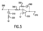
- Fig. 5 shows filter 200 for use with the embodiment of Fig. 4.
- the output of the LMX2330L is a digital charge pump
- that output 500 is first integrated by resistor 520 and capacitor 510 .
- the resulting signal is filtered by op amp 530 through resistor 540 and the network comprised of resistor 550 and capacitor 560 .
- the resulting tuning output is present at 570 .
Applications Claiming Priority (2)
| Application Number | Priority Date | Filing Date | Title |
|---|---|---|---|
| US490742 | 2000-01-25 | ||
| US09/490,742 US6922402B1 (en) | 2000-01-25 | 2000-01-25 | Mutual frequency locking across a link |
Publications (2)
| Publication Number | Publication Date |
|---|---|
| EP1120922A2 true EP1120922A2 (de) | 2001-08-01 |
| EP1120922A3 EP1120922A3 (de) | 2002-09-11 |
Family
ID=23949262
Family Applications (1)
| Application Number | Title | Priority Date | Filing Date |
|---|---|---|---|
| EP01300377A Withdrawn EP1120922A3 (de) | 2000-01-25 | 2001-01-17 | Nachrichtenverbindung |
Country Status (3)
| Country | Link |
|---|---|
| US (1) | US6922402B1 (de) |
| EP (1) | EP1120922A3 (de) |
| JP (1) | JP2001251210A (de) |
Cited By (2)
| Publication number | Priority date | Publication date | Assignee | Title |
|---|---|---|---|---|
| EP1456964A2 (de) * | 2001-12-18 | 2004-09-15 | Trex Enterprises Corporation | Drahtloses kommunikationssystem mit hoher datenrate |
| US7994899B2 (en) | 2006-06-30 | 2011-08-09 | Fujitsu Limited | Information access system and method for accessing information in contactless information storage device |
Families Citing this family (11)
| Publication number | Priority date | Publication date | Assignee | Title |
|---|---|---|---|---|
| JP4799054B2 (ja) | 2005-06-03 | 2011-10-19 | 富士通株式会社 | 情報アクセス・システムおよびアクティブ型非接触情報記憶装置 |
| JP4817768B2 (ja) * | 2005-09-07 | 2011-11-16 | 富士通株式会社 | 情報アクセス・システムおよびアクティブ型非接触情報記憶装置 |
| JP4952169B2 (ja) * | 2006-09-26 | 2012-06-13 | 富士通株式会社 | 情報アクセス・システムおよびアクティブ型非接触情報記憶装置 |
| JP4910629B2 (ja) * | 2006-10-26 | 2012-04-04 | 富士通株式会社 | 情報アクセス・システム、読取り書込み装置およびアクティブ型非接触情報記憶装置 |
| JP5023673B2 (ja) | 2006-11-24 | 2012-09-12 | 富士通株式会社 | 情報アクセス・システム、読取り書込み装置およびアクティブ型非接触情報記憶装置 |
| WO2008146494A1 (ja) * | 2007-05-29 | 2008-12-04 | Mitsubishi Electric Corporation | キャリブレーション方法、通信システム、周波数制御方法および通信装置 |
| WO2008149422A1 (ja) | 2007-06-05 | 2008-12-11 | Fujitsu Limited | センサによる検出値を蓄積するアクティブ非接触情報記憶装置 |
| JP4698755B2 (ja) * | 2007-06-27 | 2011-06-08 | 富士通株式会社 | 情報アクセス・システム、非接触読取り書込み装置、および非接触情報記憶装置 |
| JP5141173B2 (ja) * | 2007-10-05 | 2013-02-13 | 富士通株式会社 | 読取り書込み装置との間で無線通信が可能な情報装置、プログラムおよび方法 |
| JP5251110B2 (ja) * | 2007-12-18 | 2013-07-31 | 富士通株式会社 | 情報アクセス・システム、情報装置、読取り書込み装置、およびプログラム |
| JP5266762B2 (ja) * | 2008-01-11 | 2013-08-21 | 富士通株式会社 | 情報アクセス・システム、情報装置、プログラムおよび方法 |
Citations (1)
| Publication number | Priority date | Publication date | Assignee | Title |
|---|---|---|---|---|
| US4759078A (en) * | 1986-11-14 | 1988-07-19 | Rose Communication Systems, Inc. | Coordinated local oscillator receiving system |
Family Cites Families (4)
| Publication number | Priority date | Publication date | Assignee | Title |
|---|---|---|---|---|
| US5526527A (en) * | 1993-10-01 | 1996-06-11 | Pacific Communication Sciences, Inc. | Method and apparatus for frequency synthesization in digital cordless telephones |
| US5640431A (en) * | 1995-03-10 | 1997-06-17 | Motorola, Inc. | Method and apparatus for offset frequency estimation for a coherent receiver |
| US5995812A (en) * | 1995-09-01 | 1999-11-30 | Hughes Electronics Corporation | VSAT frequency source using direct digital synthesizer |
| US6442374B1 (en) * | 1998-11-04 | 2002-08-27 | Lockheed Martin Corporation | Method and apparatus for high frequency wireless communication |
-
2000
- 2000-01-25 US US09/490,742 patent/US6922402B1/en not_active Expired - Fee Related
-
2001
- 2001-01-17 EP EP01300377A patent/EP1120922A3/de not_active Withdrawn
- 2001-01-23 JP JP2001014941A patent/JP2001251210A/ja active Pending
Patent Citations (1)
| Publication number | Priority date | Publication date | Assignee | Title |
|---|---|---|---|---|
| US4759078A (en) * | 1986-11-14 | 1988-07-19 | Rose Communication Systems, Inc. | Coordinated local oscillator receiving system |
Non-Patent Citations (2)
| Title |
|---|
| CARRALERO C ET AL: "AUTOMATIC REFERENCE OSCILLATOR TUNING STRATEGY" MOTOROLA TECHNICAL DEVELOPMENTS, MOTOROLA INC. SCHAUMBURG, ILLINOIS, US, vol. 10, 1 March 1990 (1990-03-01), pages 34-35, XP000114631 * |
| PLATTNER A ET AL: "A 60 GHZ HAND-HELD LPI-TRANSCEIVER" PROCEEDINGS OF THE EUROPEAN MICROWAVE CONFERENCE. HELSINKI, SEPT. 13 - 17, 1982, SEVENOAKS, MICROWAVE EXHIBITIONS, GB, vol. CONF. 12, 1982, pages 540-544, XP000815789 * |
Cited By (3)
| Publication number | Priority date | Publication date | Assignee | Title |
|---|---|---|---|---|
| EP1456964A2 (de) * | 2001-12-18 | 2004-09-15 | Trex Enterprises Corporation | Drahtloses kommunikationssystem mit hoher datenrate |
| EP1456964A4 (de) * | 2001-12-18 | 2006-03-22 | Trex Entpr Corp | Drahtloses kommunikationssystem mit hoher datenrate |
| US7994899B2 (en) | 2006-06-30 | 2011-08-09 | Fujitsu Limited | Information access system and method for accessing information in contactless information storage device |
Also Published As
| Publication number | Publication date |
|---|---|
| EP1120922A3 (de) | 2002-09-11 |
| JP2001251210A (ja) | 2001-09-14 |
| US6922402B1 (en) | 2005-07-26 |
Similar Documents
| Publication | Publication Date | Title |
|---|---|---|
| US5390185A (en) | Transmission system for a combination of a main signal and an auxiliary signal | |
| EP0333419B1 (de) | Sender-Empfänger | |
| US5390348A (en) | System for tracking and correcting drift and dispersion in satellite transmission signals | |
| AU663122B2 (en) | Process for digital transmission and direct conversion receiver | |
| US5163159A (en) | Dual mode automatic frequency control | |
| US6922402B1 (en) | Mutual frequency locking across a link | |
| US7302236B2 (en) | Radio communication method and system for performing communication among a plurality of radio communication terminals | |
| US5550865A (en) | Frequency modulator for data transceiver | |
| US6034990A (en) | Digital radio transmission and reception system applying a direct modulation and demodulation method | |
| EP0697155B1 (de) | Drahtloser Datensendeempfänger | |
| EP0546088A1 (de) | Frequenzmodulierter synthesierer mit niederfrequentem offset-gemischtem vco | |
| EP0046682B1 (de) | Einkanaliges Duplex-Nachrichtensystem | |
| EP0135816B1 (de) | Sende- und Empfangssystem für Signale | |
| CA2118810C (en) | Radio having a combined pll and afc loop and method of operating the same | |
| KR20030010660A (ko) | 마이크로파 신호 트랜시버 내의 자체-적응식 주파수대역-통과 필터링 디바이스 | |
| US5267074A (en) | Coherent optical heterodyne transmission system | |
| EP1215822A1 (de) | Funkübertragungsgerät und Verfahren für die Einstellung von Parametern davon | |
| JPH0983583A (ja) | Fsk通信装置 | |
| EP0438832B1 (de) | Kohärentes optisches Überlagerungsübertragungssystem | |
| US3939407A (en) | Plural channel communications system | |
| JPH04245814A (ja) | Fm送信回路 | |
| KR101231381B1 (ko) | 위상 보상 시스템 | |
| KR100516354B1 (ko) | 주파수 오차 보정형 송수신장치 | |
| EP0592041A1 (de) | Übertragungssystem für ein Hauptsignal und ein Hilfssignal | |
| JPH04346525A (ja) | コヒーレント光伝送装置 |
Legal Events
| Date | Code | Title | Description |
|---|---|---|---|
| PUAI | Public reference made under article 153(3) epc to a published international application that has entered the european phase |
Free format text: ORIGINAL CODE: 0009012 |
|
| AK | Designated contracting states |
Kind code of ref document: A2 Designated state(s): AT BE CH CY DE DK ES FI FR GB GR IE IT LI LU MC NL PT SE TR |
|
| AX | Request for extension of the european patent |
Free format text: AL;LT;LV;MK;RO;SI |
|
| RAP1 | Party data changed (applicant data changed or rights of an application transferred) |
Owner name: AGILENT TECHNOLOGIES INC. A DELAWARE CORPORATION |
|
| RAP1 | Party data changed (applicant data changed or rights of an application transferred) |
Owner name: AGILENT TECHNOLOGIES, INC. (A DELAWARE CORPORATION |
|
| PUAL | Search report despatched |
Free format text: ORIGINAL CODE: 0009013 |
|
| AK | Designated contracting states |
Kind code of ref document: A3 Designated state(s): AT BE CH CY DE DK ES FI FR GB GR IE IT LI LU MC NL PT SE TR |
|
| AX | Request for extension of the european patent |
Free format text: AL;LT;LV;MK;RO;SI |
|
| RIC1 | Information provided on ipc code assigned before grant |
Free format text: 7H 04B 1/52 A, 7H 03D 3/24 B, 7H 04B 1/40 B |
|
| 17P | Request for examination filed |
Effective date: 20030311 |
|
| AKX | Designation fees paid |
Designated state(s): DE FR GB |
|
| RAP1 | Party data changed (applicant data changed or rights of an application transferred) |
Owner name: AGILENT TECHNOLOGIES, INC. |
|
| STAA | Information on the status of an ep patent application or granted ep patent |
Free format text: STATUS: THE APPLICATION IS DEEMED TO BE WITHDRAWN |
|
| 18D | Application deemed to be withdrawn |
Effective date: 20070801 |