EP1119290B1 - Ensemble detecteurs a etages - Google Patents
Ensemble detecteurs a etages Download PDFInfo
- Publication number
- EP1119290B1 EP1119290B1 EP99953007A EP99953007A EP1119290B1 EP 1119290 B1 EP1119290 B1 EP 1119290B1 EP 99953007 A EP99953007 A EP 99953007A EP 99953007 A EP99953007 A EP 99953007A EP 1119290 B1 EP1119290 B1 EP 1119290B1
- Authority
- EP
- European Patent Office
- Prior art keywords
- detector
- ray
- sub
- elements
- photon
- Prior art date
- Legal status (The legal status is an assumption and is not a legal conclusion. Google has not performed a legal analysis and makes no representation as to the accuracy of the status listed.)
- Expired - Lifetime
Links
- 229910052710 silicon Inorganic materials 0.000 claims abstract description 14
- 239000010703 silicon Substances 0.000 claims abstract description 14
- 238000000034 method Methods 0.000 claims abstract description 11
- 239000000758 substrate Substances 0.000 claims description 20
- 239000000463 material Substances 0.000 claims description 15
- XUIMIQQOPSSXEZ-UHFFFAOYSA-N Silicon Chemical compound [Si] XUIMIQQOPSSXEZ-UHFFFAOYSA-N 0.000 claims description 13
- 238000003491 array Methods 0.000 claims description 7
- QWUZMTJBRUASOW-UHFFFAOYSA-N cadmium tellanylidenezinc Chemical compound [Zn].[Cd].[Te] QWUZMTJBRUASOW-UHFFFAOYSA-N 0.000 claims description 2
- 239000013078 crystal Substances 0.000 abstract description 17
- 238000003384 imaging method Methods 0.000 abstract description 12
- 238000010894 electron beam technology Methods 0.000 description 8
- 230000004907 flux Effects 0.000 description 8
- 238000001514 detection method Methods 0.000 description 7
- 238000010586 diagram Methods 0.000 description 7
- BASFCYQUMIYNBI-UHFFFAOYSA-N platinum Chemical compound [Pt] BASFCYQUMIYNBI-UHFFFAOYSA-N 0.000 description 6
- 238000005259 measurement Methods 0.000 description 4
- 238000009826 distribution Methods 0.000 description 3
- PCHJSUWPFVWCPO-UHFFFAOYSA-N gold Chemical compound [Au] PCHJSUWPFVWCPO-UHFFFAOYSA-N 0.000 description 3
- 229910052737 gold Inorganic materials 0.000 description 3
- 239000010931 gold Substances 0.000 description 3
- 229910052738 indium Inorganic materials 0.000 description 3
- APFVFJFRJDLVQX-UHFFFAOYSA-N indium atom Chemical compound [In] APFVFJFRJDLVQX-UHFFFAOYSA-N 0.000 description 3
- 229910052697 platinum Inorganic materials 0.000 description 3
- 239000007787 solid Substances 0.000 description 3
- MARUHZGHZWCEQU-UHFFFAOYSA-N 5-phenyl-2h-tetrazole Chemical compound C1=CC=CC=C1C1=NNN=N1 MARUHZGHZWCEQU-UHFFFAOYSA-N 0.000 description 2
- 230000005540 biological transmission Effects 0.000 description 2
- 230000000694 effects Effects 0.000 description 2
- 238000001914 filtration Methods 0.000 description 2
- 230000033001 locomotion Effects 0.000 description 2
- 239000007769 metal material Substances 0.000 description 2
- 230000008569 process Effects 0.000 description 2
- 238000012545 processing Methods 0.000 description 2
- 239000011669 selenium Substances 0.000 description 2
- 230000035945 sensitivity Effects 0.000 description 2
- 238000012360 testing method Methods 0.000 description 2
- BUGBHKTXTAQXES-UHFFFAOYSA-N Selenium Chemical compound [Se] BUGBHKTXTAQXES-UHFFFAOYSA-N 0.000 description 1
- 238000010521 absorption reaction Methods 0.000 description 1
- 230000008901 benefit Effects 0.000 description 1
- 230000001419 dependent effect Effects 0.000 description 1
- 238000002059 diagnostic imaging Methods 0.000 description 1
- 238000011835 investigation Methods 0.000 description 1
- 230000007246 mechanism Effects 0.000 description 1
- 238000012986 modification Methods 0.000 description 1
- 230000004048 modification Effects 0.000 description 1
- 239000002245 particle Substances 0.000 description 1
- 238000002360 preparation method Methods 0.000 description 1
- 230000026954 response to X-ray Effects 0.000 description 1
- 229910052711 selenium Inorganic materials 0.000 description 1
- 239000004065 semiconductor Substances 0.000 description 1
- 238000001228 spectrum Methods 0.000 description 1
- 230000000007 visual effect Effects 0.000 description 1
Images


Classifications
-
- G—PHYSICS
- G01—MEASURING; TESTING
- G01T—MEASUREMENT OF NUCLEAR OR X-RADIATION
- G01T1/00—Measuring X-radiation, gamma radiation, corpuscular radiation, or cosmic radiation
- G01T1/16—Measuring radiation intensity
- G01T1/24—Measuring radiation intensity with semiconductor detectors
- G01T1/243—Modular detectors, e.g. arrays formed from self contained units
-
- H—ELECTRICITY
- H01—ELECTRIC ELEMENTS
- H01L—SEMICONDUCTOR DEVICES NOT COVERED BY CLASS H10
- H01L27/00—Devices consisting of a plurality of semiconductor or other solid-state components formed in or on a common substrate
- H01L27/14—Devices consisting of a plurality of semiconductor or other solid-state components formed in or on a common substrate including semiconductor components sensitive to infrared radiation, light, electromagnetic radiation of shorter wavelength or corpuscular radiation and specially adapted either for the conversion of the energy of such radiation into electrical energy or for the control of electrical energy by such radiation
- H01L27/144—Devices controlled by radiation
- H01L27/146—Imager structures
- H01L27/14665—Imagers using a photoconductor layer
- H01L27/14676—X-ray, gamma-ray or corpuscular radiation imagers
Definitions
- the present invention pertains to the field of detectors including, more specifically, to detectors capable of use in imaging systems.
- an output signal from a detector is applied to the z-axis (luminance) input of a video monitor.
- This signal modulates the brightness of the viewing screen.
- the x and y inputs to the video monitor are typically derived from the signal that effects deflection of the electron beam of an x-ray tube. Therefore, the luminance of a point on the viewing screen is inversely proportional to the absorption of x-rays passing from the source, through the object, to the detector.
- the randomness is typically expressed as the standard deviation of the mean flux, and equals its square root.
- the signal-to-noise ratio of a x-ray image under these conditions is equal to the mean flux divided by the square root of the mean flux. i.e., for a mean flux of 100 photons, the noise is +/- 10 photons, and the signal-to-noise ratio is 10.
- the spatial resolution of the resulting image is in large part determined by the capture area of one of the detector elements.
- a non-segmented detector with a small capture area can provide high spatial resolution and poor collection efficiency (i.e., the ratio of the meaningful photons passing through the object to the total number of photons passing through the object), while a non-segmented detector with a large capture area provides high collection efficiency and poor spatial resolution.
- a medical imaging system should provide low patient dosage, high spatial resolution and a refresh rate of up to about 30 times per second which is the refresh rate of a standard video display -- all at the same time.
- the spatial resolution and the signal-to-noise ratio of x-ray images formed by known reverse-geometry x-ray imaging systems are dependent, to a large extent, upon the size of the sensitive area of the detector element. If the sensitive area of the detector element in these systems is increased, more of the diverging rays are detected, effectively increasing sensitivity and improving the signal-to-noise ratio.
- larger detector areas tend to reduce the attainable spatial resolution as the "pixel" size (measured at the plane of the object to be imaged) becomes larger. This is so because of the distance typical objects to be imaged in some medical applications (e.g., structures internal to the human body) are from the x-ray source.
- Solid state x-ray detectors for x-ray imaging systems like the ones disclosed in WO98/05980 and WO98/29904 , are known.
- An example of a solid state x-ray detector is disclosed in U.S. Patent 5,379,336 to Kramer et al.
- Kramer et al. discloses a hybrid detector array with many thousands of individual detector pixels on a single semiconductor substrate interconnected to a corresponding readout with individual amplifiers and signal condition circuits for each pixel and multiplexor output.
- the detector pixels of the type disclosed in Kramer et al. generate electrical signals in response to x-ray photons.
- the detector pixels disclosed in Kramer et al. are 30 ⁇ m by 30 ⁇ m.
- detector pixels are therefore of a small size to increase spatial resolution.
- One problem associated with having detector pixels of a small size is that more than one detector pixel in a given area may be effected by a single x-ray photon. This situation can affect the accuracy of an image of an object under investigation.
- the present invention is directed to a detector array having a plurality of detector elements comprising a plurality of detector sub-elements.
- the outputs of the detector sub-elements are connected to summing circuitry which outputs a signal indicative of the number of photons striking the detector element.
- the plurality of detector elements, sub-elements and summing circuitry are mounted on a single substrate.
- the detector assembly comprises tiered detector arrays wherein each tier comprises a plurality of detectors.
- the detector array is formed by combining a plurality of detectors into an array of detectors.
- the detector array has a multi-tiered structure, each tier having at least one detector, and each tier in a different plane than any other tier.
- a method for generating x-ray transmissiveness information comprises directing an x-ray beam from an x-ray source to a detector assembly; generating an electrical signal indicative of the energy level of a photon energizing a detector sensor; determining whether the electrical signal is a valid detection; comparing the valid detection with at least one other detector and precluding erroneous detections.
- FIG. 1 is a diagram showing components of a x-ray imaging system embodying aspects of the invention.
- X-ray source 10 preferably includes an electron beam source comprising a power supply which can operate x-ray source 10 at about -70kV to -120kV. In the present embodiment, this voltage level preferably produces a spectrum of x-rays ranging to 120 keV.
- Electron beam 40 which is generated within x-ray source 10 by a charged particle gun, is deflected over the surface of a target assembly 50 in a predetermined pattern, e.g., a scanning or stepping pattern.
- X-ray source 10 also preferably includes a mechanism to control the movement of electron beam 40 across target assembly 50, such as a deflection yoke 20 under the control of an electron beam pattern generator 30.
- a mechanism to control the movement of electron beam 40 across target assembly 50 such as a deflection yoke 20 under the control of an electron beam pattern generator 30.
- One advantage provided by the geometry of x-ray source 10 is that it allows x-rays to be projected at an object 100 from multiple angles without requiring physical relocation of the x-ray source 10.
- a presently preferred method and apparatus for generating and moving electron beam 40 across target assembly 50 is disclosed in commonly owned U.S. Patent No. 5,644,612 .
- a collimating assembly is located between x-ray source 10 and a tiered detector assembly 60.
- the collimating assembly is located between x-ray source 10 and the object 100 to be imaged.
- the number of apertures 80 in collimator grid 70 corresponds to the number of image pixels that are to be displayed on monitor 140 or other visual display devices that can be connected to the video output of the x-ray imaging system.
- the image pixel to aperture ratio is increased, so that the number of apertures are less than the number of image pixels that are displayed on a display device.
- An "object pixel,” for purposes of this discussion, is an area in a plane of the object about which information is being collected.
- An image pixel is a picture element that is an image representation of one or more object pixels.
- the presently preferred number of apertures is 10,000 arranged in a 100 by 100 grid.
- the number of apertures suggested above is for illustrative purpose only and depends on the particular application to which the invention is directed.
- An example of a collimator grid that can be utilized in the invention is disclosed in U.S. Patent No. 5,610,967 .
- electron beam 40 preferably dwells at a location 110 on target assembly 50 which is located substantially at a position where the axis 90 for a particular aperture 120 of collimator grid 70 intersects the target assembly 50.
- a cascade of x-rays 130 is emitted. Only the portion of the cascade of x-rays 130 whose path lies substantially along axis 90 pass through aperture 120 and form a diverging x-ray beam 135.
- the shape of x-ray beam 135 is influenced by the shape of aperture 120. For instance, if the aperture is square, the x-ray beam 135 takes on a generally truncated pyramidal shape.
- x-ray beam 135 takes on a generally conical shape.
- the shape and area of the aperture is such that the area of maximum divergence of the x-ray beam 135 is substantially the same as the dimensions of the x-ray capture surface for multi-detector array 60 and the axis 90 passes through the geometric center of the tiered detector assembly 60.
- Tiered detector assembly 60 preferably comprises a plurality of tiers of detector arrays. Each tier preferably comprises detector elements 61 arranged in an array. Each detector element 61 preferably provides discrete information indicative of the number of x-ray photons that energize the x-ray sensing surface.
- Each detector element 61 preferably provides discrete information indicative of the number of x-ray photons that energize the x-ray sensing surface.
- each detector element comprises components for determining the quantity of x-ray photons that strike x-ray sensing surface of the detector element and outputting a signal indicative of that determination.
- each detector element includes components for determining the energy of the x-rays that strike x-ray sensing surface of the detector element.
- the tiered detector assembly 60 outputs transmissiveness information that is proportional to the x-ray transmission of the object 100 along particular x-ray beam subpaths.
- the x-ray transmission information can be used in creating an image representative of object 100, i.e. a representation of the x-ray transmissiveness of object 100, which can be displayed on monitor 140.
- the presently preferred tiered detector assembly is disclosed and described herein.
- image reconstruction system 65 X-ray transmissiveness information obtained from the detector elements 61 pertinent to specific image pixels are reconstructed by image reconstruction system 65.
- image reconstruction system 65 also performs control functions and display preparation for the x-ray imaging system. Operational instructions and control of the x-ray source 10, detector 60 and image reconstruction system 65 are preferably made through a control workstation 150. Control workstation 150 also preferably receives operational and status information from the various components of the x-ray imaging system.
- FIG. 2 depicts a block diagram of an embodiment of a preferred image reconstruction system 65.
- the image reconstruction system 65 comprises a PCI interface 210, which connects to control workstation 150.
- a detection module 200 includes a tiered detector assembly 60 and receives x-ray transmissiveness information. Detection module 200 also comprises components to receive data signals from the tiered detector assembly.
- Image reconstruction chassis 205 preferably comprises an interface module 215, one or more plane reconstruction modules 220, an image selection module 230 and an image preprocessor 235.
- the various components on the image reconstruction chassis 205 are preferably interconnected via one or more busses 225, which also include control lines.
- PCI interface 210 and detection module 200 are preferably coupled to interface module 215, whereas image preprocessor 235 is coupled to video post processor 245.
- Video post processor 245 is coupled to display monitors 240.
- a x-ray beam 130 illuminates a collimator aperture 120 for approximately 1.04 ⁇ S measurement period.
- a dead time of 0.24 ⁇ S occurs as the scanning beam x-ray source 10 moves the x-ray beam to the next collimator aperture.
- the collimator apertures 80 are scanned row-by-row, but in a pattern that repeats each row 2, 4, or 8 times, depending on the number of collimator apertures 80.
- a frame is scanned every 33.33 mS.
- FIG. 3A depicts a top view of a detector array board 300.
- Each detector array 310 preferably comprises four detectors 312.
- Processing and filtering electronics for the detectors are preferably contained on printed circuit board 314.
- the printed circuit board 314 and detector 310 are supported by a chassis 316.
- the chassis 316 comprises a plurality of mounting holes 318.
- FIG. 3B is a front elevation view of detector array board 300.
- Card connector 320 extends the length of the detector array board 300, and is used to connect consecutive detector array boards and electronic cards.
- FIG. 3C shows a side elevation view of the detector array board 300.
- FIG. 4A is a top view of four detector array boards 300, 302, 304 and 306 stacked in a terraced fashion, together which comprise a multi-tiered detector array 400.
- detectors on each of the detector array boards are the same, reference numbers have been given to the detectors on detector array board 300 and 306 as detector 312 and 410 depict.
- Detector 410 is preferably no different from detector 312, except that it detects x-rays at a different location in the multi-detector array 400.
- FIG. 4B is a front elevation view of the multi-tiered detector array 400. Visible in FIG. 4B are side profiles of each of the four rows of detectors. Electronics card 412 is shown inserted into slot 321 of card connector 320. Electronics card 412 includes circuitry for filtering and processing transmissivity data detected at the detector arrays. There is one electronics card 412 for each detector array board 300, 302, 304 and 306. FIG. 4C depicts a side view of the same.
- FIG. 5 is a bottom view of a presently most preferred tiered multi-detector and electronics assembly 500.
- Walls 504 have a plurality of card guides 520, which receive and align electronics cards 412, shown in Fig. 4C .
- Mounting surface 508 comprises a support structure having four steps 512, which each support a detector array board, for example detector array boards 300 and 306. Each step 512 is staggered, or tiered, a distance that allows the stacking of the detector array boards while leaving a small clearance between the detector array boards; preferably the distance is 0.170 inches.
- a screw 516 and washer assembly 524 securely attach the detector array boards to the mounting surface 508 at screw holes 528.
- detector 410 Just visible at the front edge of detector array board 306 is detector 410, which gives a frame of reference back to the figures described above.
- the multi-detector assembly 500 is located in the x-ray imaging system so that it receives x-ray transmissivity information concerning an imaged object, as a result of x-rays emitted from the x-ray source (e.g., x-ray source 10).
- the sixteen detectors face the x-ray source from detector opening 540.
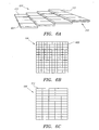
- FIGS. 6A-C depict a varying levels of detail of the multi-detector array according to a preferred embodiment of the present invention.
- the presently preferred shape and area of the detector elements is such that it is statistically likely that the detection surface of any detector element 61 in the preferred multi-detector array 60 will receive at most seven x-ray photons per x-ray path.
- the statistical calculations are based upon the Poisson distribution and the area of the detector elements.
- FIG. 6A depicts a perspective view of a tiered-array 600 of detectors, showing the preferred terracing of the one by four arrays of detectors.
- the tiered-array 600 of detectors is approximately 54.72 mm square (thus, an area of approximately 2994 mm 2 ).
- FIG. 7 depicts the presently preferred detector 604. It should be noted that FIG. 7 is not to scale, nor are the dimensions the preferred dimensions of the detector 604.
- Detector 604 is preferably a solid state detector comprised of a single substrate and preferably a single piece of silicon and a single piece of x-ray sensitive material, preferably an x-ray sensitive crystal and more preferably a crystal comprising Cadmium Zinc Telluride.
- the electrical interconnection between the silicon substrate 704 and the x-ray sensitive crystal 708 is preferably formed by a process known as bump bonding.
- a plurality of electrodes or "bond pads" 716 preferably of a metal material and more preferably of a platinum or gold, are formed on one surface of the silicon substrate.
- a plurality of bond pads are added to one surface of the CdZTe crystal 708.
- Indium bumps 712 are preferably deposited on the bond pads 716 of both the silicon substrate 704 and the CdZTe crystal 708.
- the indium bumps 712 form an electrical connection between the bond pads on the silicon substrate 704 and the CdZTe crystal 708.
- a thin layer of platinum or gold 709 is deposited on the active surface, i.e., the surface that receives the x-ray photons, of the x-ray sensitive crystal.
- the bond pads 716 on both the silicon substrate 704 and the CdZTe crystal 708 are preferably arranged in a 60 x 144 array. Because of the characteristics of the x-ray sensitive crystal 708 this effectively creates an array of 60 x 144 detector sub-elements. As is shown in FIG. 6B and 6C , in the most preferred embodiment these detector sub-elements 612 are preferably grouped into detector elements 608. Preferably there are 60 detector sub-elements 612 that comprise each detector element 608. As will be explained below this grouping into detector elements is accomplished through the summing circuitry. As seen in Figure 6B and 6C the array of detector sub-elements forming a detector is preferably a 5 x 12 array. As seen in Figure 6B , preferably the array of detector elements is a 12 x 12 array. It should be noted that the number and shape of the arrays may vary and may take any geometric shape for a particular application. This is an advantageous configuration for medical applications.
- Each detector element 608 is approximately 1.125 mm square (thus, an area of approximately 1.266 mm 2 ). Due to the characteristics of the CdZTe crystal material and the arrangement of the bond pads 716, each detector sub-element 612 is effectively a rectangle of approximately 93 ⁇ m by 228 ⁇ m. Since there are preferably 60 detector sub-elements 612 in each detector element 608, and there are preferably 144 elements 608 in a detector 604, there are (5x12x12x12) 8640 detector sub-elements 612 in a single detector 604 and 138,240 sub-elements 612 in a preferred tiered detector assembly 60.
- a top row of detector sub-elements 612 on the top row of detector elements 608 in each array of detectors (e.g. detector array 310) on each detector array board 306, and the bottom row of sub-elements 612 on the bottom row of elements 608 in each array of detectors on each detector array board 306, are not utilized for detecting x-ray photons to accommodate the tiered array 600 of detectors.
- the CdZTe crystal 708 is presently preferred to convert the x-ray photons to an electrical signal.
- other materials such as Selenium (Se) or Cadmium Telluride (CdTe) can also be used, since they too are capable of sensing the x-ray photons and converting the photons into an electrical signal.
- FIG. 8 depicts a block diagram of circuitry comprising the detector sub-element electronics 800.
- the detector sub-element electronics 800 comprises an x-ray photon sensor 804, an amplifier 808, a discriminator 812, and a digital-to-analog (D/A) converter 824.
- the x-ray photon sensor is the portion of the CdZTe crystal defined by a bond pad 716.
- the digital-to-analog converter further comprises a veto circuit.
- the sensor 804 As x-ray photons strike the sensor 804, electron hole pairs are created, that is, it breaks electrons away from atoms leaving behind holes. The number of electron hole pairs generated is a product of the energy of the x-ray photons. The higher the photon energy, the more electron hole pairs will be generated.
- the sensor 804, which comprises a crystal, has a voltage across it and hence an electron field across it. Motion of the electrons and the holes induces a charge on conducting line 806. This charge is amplified by the resetable amplifier 808.
- the conducting line 806 comprises the bond pad 716 on the CdZTe crystal 708, the indium bump bond 712, the bond pad 716 on the silicon substrate 704 and the electrical trace on the silicon substrate 704.
- An amplified signal is output from amplifier 808 via conducting line 810 and is fed into a discriminator 812.
- the discriminator 812 compares the amplified signal from conducting line 810 to a threshold value 816.
- a threshold value 816 10 to 120 keV photons are measured. Accordingly, x-ray photons with less than 10 keV are removed.
- the threshold value 816 is equivalent to 10 to 15 keV, so an equivalent amount of electrons are set as the threshold value.
- the threshold value 816 is between 2000 and 3000 electrons.
- the threshold value 816 is adjustable. If the measured energy level exceeds the threshold value, then a TRUE signal is output to conducting line 820. If the threshold value is not exceeded, then a FALSE signal is output to conducting line 820.
- Digital-to-analog converter 824 is fed with the output of the discriminator 812 via conducting line 820.
- the digital-to-analog converter 824 is preferably a digital-to-current converter.
- the digital-to-analog 824 converter includes a veto circuit and a fixed output current source.
- the veto circuit accepts or rejects the input from the discriminator 812 based upon external values, or feedback from other discriminators 812.
- the veto circuit accepts as inputs a KILL signal, an input from a detector sub-element above it, and an input from a detector sub-element to the left of it. If any of these signals are TRUE, then the veto circuit rejects the TRUE signal from a discriminator 812. (Note that a FALSE signal does not need to be rejected.)
- the veto circuit minimizes the possibility of double counting of an x-ray photon. It is possible that x-ray photons incident on a particular detector sub-element will generate an electrical signal above the threshold value of nearest neighbor or next to nearest neighbor detector sub-elements of the particular detector sub-element.
- the KILL signal it is based upon external control and the result of a test of the detector sub-elements. If a particular detector sub-element is known to leak current or give erroneous readings, that is, give a TRUE signal even though x-ray photons are not striking the sub-element, then readings from that particular sub-element should be ignored, hence, a KILL signal to turn off the particular detector sub-element.
- different logic can be employed in the veto circuit if, for example, different x-ray flux levels are utilized.
- the detector sub-element electronics 800 are formed in the silicon substrate 704 in an area surrounding the bonding pad 716 and more preferably under the bonding pad 716.
- FIG. 9 depicts a block diagram of a current summing bus and an analog-to-digital converter.
- Output 904 from the 60 (or less, depending on the location) detector sub-elements e.g., output 828 of sub-element 612 are combined at summing junctions 908, which result in a summing current bus 912.
- the summing current bus 912 is essentially an analog counter, the current carried by the summing current bus 912 being representative of the number of sub-elements that sensed x-ray photons (and passed the discriminator and veto circuit tests).
- the current summing bus 912 feeds a current-to-digital converter 916.
- the current-to-digital converter 916 transforms the analog current into a three-bit digital value representing transmissiveness values 0 through 7.
- the three-bit digital value is output on a three-bit digital bus 920.
- each detector has 48 by 12 three-bit data words associated with it, which yields 48 x 48 three-bit data words for the entire preferred tiered detector and electronics assembly 600 ( FIG. 6 ).
- the summing circuitry is located in an area on the silicon substrate 704 in close proximity to the array of detector sub-elements that comprise the detector elements.
- the photons detected by the detector sub-elements 612 are preferably summed and sampled during the inter-collimator hole period and are subsequently converted to digital values by on-chip current-to-digital converters (e.g., analog-to-digital converter 916) during the next measurement period.
- the 144 sampled and digitized values are read out during the following measurement cycle, that is the cycle for the next detector (e.g., detector 312).
- the silicon substrate 704 is preferably slightly larger in one dimension than the CdZTe crystal 708.
- Contact pads 717 are preferably formed in this area for connection with the electronics on the detector array board 306.
- a measurement is made approximately every 1 ⁇ S.
- the detector element 608 is capable of counting 7 photons. This yields a sample rate on the order of 7x10 6 photons per second.
- FIGS. 10-15 are electrical schematics, employing standard electrical symbology, of various electronics described above with reference to FIGS. 8 and 9 .
- FIG. 10 is an electrical schematic of presently most preferred detector sub-element electronics 1000.
- the detector sub-element electronics 1000 receives an input from a photon sensor (not shown) at amplifier 1004.
- Amplifier 1004 in turn feeds a signal to discriminator 1008.
- Discriminator 1008 feeds an output to veto circuit 1016.
- a latch 1012 connects an input voltage to the veto circuit 1216, based upon an external signal (e.g., from a control workstation 150).
- the veto circuit 1016 turns on or off a constant current source 1020.
- FIG. 11 depicts electronics for the amplifier 1004,
- FIG. 12 depicts electronics for the discriminator 1008,
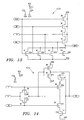
- FIG. 13 depicts electronics for veto circuit 1016, and
- FIG. 14 depicts an electronics for the latch 1012.
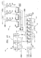
- FIG. 15 depicts an electrical schematic for the analog-to-digital converter 916 depicted in FIG. 9 which, according to a preferred embodiment, is a current-to-digital converter.
- the current from the summing bus 912 is input at terminal 1510.
- a current mirror 1520 replicates the current on line 1525.
- a counting current source 1530 generates a current corresponding to values 0-7, via counting selectors 1535. The sum of the two currents creates a voltage potential that increases to a particular point at terminal 1537.
- a comparator 1536 monitors the voltage at terminal 1537. When the voltage at terminal 1537 passes a threshold value, the value at counting selectors 1535 is latched into digital bit drivers 1540 by the comparator 1536. The result is a three-bit digital value representing discrete x-ray transmissivity information. This value is output on three-bit digital bus 1550.
Landscapes
- Spectroscopy & Molecular Physics (AREA)
- Health & Medical Sciences (AREA)
- Life Sciences & Earth Sciences (AREA)
- General Physics & Mathematics (AREA)
- High Energy & Nuclear Physics (AREA)
- Molecular Biology (AREA)
- Physics & Mathematics (AREA)
- Measurement Of Radiation (AREA)
- Forklifts And Lifting Vehicles (AREA)
- Acyclic And Carbocyclic Compounds In Medicinal Compositions (AREA)
- Rotational Drive Of Disk (AREA)
- Apparatus For Radiation Diagnosis (AREA)
- Solid State Image Pick-Up Elements (AREA)
Claims (16)
- Ensemble de détecteur de comptage de photons de rayons X (600) comprenant :au moins un détecteur, chaque détecteur comprenant au moins un élément de détecteur (608), chaque élément de détecteur comprenant :une sortie d'élément de détecteur ;un circuit de sommation ;un matériau sensible aux rayons X ; etune pluralité de sous-éléments de détecteur (612), chacun des sous-éléments de détecteur étant associé à une portion du matériau sensible aux rayons X et ayant une sortie de sous-élément de détecteur (828), le sous-élément de détecteur comprenant un circuit pour déterminer lorsqu'un photon de rayons X d'une énergie prédéterminée frappe la portion du matériau sensible aux rayons X associée à ce sous-élément de détecteur et délivrant un signal de réception de photon sur le sous-élément de détecteur indiquant quand un photon d'énergie prédéterminée frappe le matériau sensible aux rayons X associé à ce sous-élément de détecteur particulier ;toutes lesdites sorties de sous-éléments de détecteur étant couplées de manière non sélective au dit circuit de sommation ; ledit circuit de sommation sommant toutes les sorties de sous-éléments de détecteur, ledit circuit de sommation et lesdits sous-éléments de détecteur étant montés sur un substrat unique ; etla sortie du circuit de sommation formant ladite sortie d'élément de détecteur représentant le nombre de photons de ladite énergie prédéterminée.
- Ensemble de détecteur de comptage de photons de rayons X selon la revendication 1, comprenant une pluralité d'éléments de détecteur dans lequel lesdits éléments de détecteur sont agencés dans un réseau.
- Ensemble de détecteur de comptage de photons de rayons X selon la revendication 2, dans lequel lesdits sous-éléments de détecteur de chacun desdits éléments de détecteur sont agencés dans un réseau et chacun desdits réseaux d'éléments de détecteur est formé sur des substrats de silicium distincts.
- Ensemble de détecteur de comptage de photons de rayons X selon la revendication 3, dans lequel lesdits substrats sont agencés dans un réseau à étages.
- Ensemble de détecteur de comptage de photons de rayons X selon la revendication 2, dans lequel lesdits détecteurs sont agencés dans une pluralité de réseaux avec chaque réseau de détecteurs dans un plan différent.
- Ensemble de détecteur de comptage de photons de rayons X selon la revendication 1, dans lequel ledit circuit de chacun de ladite pluralité de sous-éléments de détecteur comprend :un capteur de photons de rayons X capable de délivrer un signal indicatif de l'énergie d'un photon de rayons X frappant ledit matériau sensible aux rayons X associé au dit sous-élément de détecteur ;un amplificateur, ledit amplificateur étant couplé au dit capteur de photons de rayons X pour recevoir ledit signal indicatif de l'énergie du photon de rayons X frappant ledit matériau sensible aux rayons X associé au dit sous-élément de détecteur et pour délivrer un signal d'énergie de photon amplifié ;un discriminateur, ledit discriminateur étant couplé au dit amplificateur pour recevoir ledit signal d'énergie de photon amplifié, ledit discriminateur étant configuré pour être capable de déterminer si ledit signal d'énergie de photon amplifié dudit amplificateur est supérieur ou égal à un seuil prédéterminé, ledit seuil prédéterminé représentant ladite énergie prédéterminée, et pour délivrer un signal de réception de photon indiquant qu'un photon de rayons X supérieur ou égal à ladite énergie prédéterminée a été reçu par ledit sous-élément de détecteur en tant que ladite sortie de sous-élément de détecteur.
- Ensemble de détecteur de comptage de photons de rayons X selon la revendication 6, dans lequel ledit circuit de sommation comprend un bus de sommation analogique (912), ledit bus de sommation analogique étant configuré pour combiner lesdites sorties de sous-éléments de détecteur.
- Ensemble de détecteur de comptage de photons de rayons X selon la revendication 6, dans lequel lesdits sous-éléments de détecteur comprennent en outre un circuit de veto, ledit circuit de veto étant connecté au dit discriminateur, ledit circuit de veto étant configuré pour empêcher le double comptage d'un photon de rayons X.
- Ensemble de détecteur de comptage de photons de rayons X selon la revendication 1, dans lequel ledit matériau sensible aux rayons X comprend du tellurure de zinc et de cadmium.
- Ensemble de détecteur de comptage de photons de rayons X selon la revendication 3, dans lequel ledit matériau sensible aux rayons X est lié par bosses au dit substrat.
- Ensemble de détecteur de comptage de photons de rayons X selon la revendication 10, dans lequel ladite pluralité de sous-éléments est définie par un réseau de patins de liaisons de bosses.
- Ensemble de détecteur de comptage de photons de rayons X selon la revendication 3, dans lequel ledit substrat est plus grand que ledit matériau sensible aux rayons X.
- Procédé de comptage de photons de rayons X frappant un matériau sensible aux rayons X d'un élément de détecteur ; dans lequel l'élément de détecteur comprend une pluralité de sous-éléments de détecteur ; le matériau sensible aux rayons X est divisé en une pluralité de sous-zones, chaque sous-zone étant associée à l'un des sous-éléments de détecteur, et les sous-éléments de détecteur comprennent un circuit ; comprenant les actes consistant à :générer un signal d'énergie de photon indicatif d'une quantité d'énergie de chaque photon de rayons X qui frappe chaque sous-zone ;comparer chaque signal d'énergie de photon à une valeur de seuil, dans lequel la valeur de seuil est une valeur représentative de l'énergie d'un photon de rayons X unique qui est compté ;générer un signal de réception de photon de rayons X si le signal d'énergie de photon est supérieur ou égal à la valeur de seuil ;sommer tous les signaux de réception de photon de rayons X et générer un signal sommé indicatif du nombre de sous-zones qui ont été frappées par un photon de rayons X ; etdélivrer le signal sommé.
- Procédé selon la revendication 13, dans lequel la génération d'un signal de réception de photons est effectuée environ toutes les 1 µs.
- Procédé selon la revendication 13, dans lequel un réseau de détecteur à étages est utilisé.
- Procédé selon la revendication 13, dans lequel les actes consistant à générer et à comparer sont effectués par le circuit de sous-éléments de détecteur et les sous-éléments de détecteur sont montés sur une bosse de substrat unique liée au matériau sensible aux rayons X.
Applications Claiming Priority (3)
| Application Number | Priority Date | Filing Date | Title |
|---|---|---|---|
| US09/167,318 US6175611B1 (en) | 1998-10-06 | 1998-10-06 | Tiered detector assembly |
| US167318 | 1998-10-06 | ||
| PCT/US1999/022784 WO2000019898A1 (fr) | 1998-10-06 | 1999-09-30 | Ensemble detecteurs a etages |
Publications (3)
| Publication Number | Publication Date |
|---|---|
| EP1119290A1 EP1119290A1 (fr) | 2001-08-01 |
| EP1119290A4 EP1119290A4 (fr) | 2001-12-19 |
| EP1119290B1 true EP1119290B1 (fr) | 2008-11-12 |
Family
ID=22606873
Family Applications (1)
| Application Number | Title | Priority Date | Filing Date |
|---|---|---|---|
| EP99953007A Expired - Lifetime EP1119290B1 (fr) | 1998-10-06 | 1999-09-30 | Ensemble detecteurs a etages |
Country Status (8)
| Country | Link |
|---|---|
| US (1) | US6175611B1 (fr) |
| EP (1) | EP1119290B1 (fr) |
| JP (1) | JP2002526751A (fr) |
| AT (1) | ATE413839T1 (fr) |
| AU (1) | AU6504599A (fr) |
| DE (1) | DE69939904D1 (fr) |
| IL (1) | IL142297A0 (fr) |
| WO (1) | WO2000019898A1 (fr) |
Cited By (2)
| Publication number | Priority date | Publication date | Assignee | Title |
|---|---|---|---|---|
| CN106483548A (zh) * | 2015-08-28 | 2017-03-08 | 北京纳米维景科技有限公司 | 一种光子计数探测器阵列及其成像方法 |
| EP4086666A3 (fr) * | 2021-05-04 | 2023-02-15 | Siemens Medical Solutions USA, Inc. | Détecteur de rayons gamma tridimensionnel inclinable |
Families Citing this family (27)
| Publication number | Priority date | Publication date | Assignee | Title |
|---|---|---|---|---|
| JP3347708B2 (ja) * | 1999-08-04 | 2002-11-20 | キヤノン株式会社 | 2次元画像入力装置及びそれを用いた画像処理システム |
| JP3208426B2 (ja) | 1999-09-14 | 2001-09-10 | 経済産業省産業技術総合研究所長 | 高速x線ctによる被写移動体速度及び高解像度情報の計測方法及びその装置 |
| GB0103133D0 (en) * | 2001-02-08 | 2001-03-28 | Univ Glasgow | Improvements on or relating to medical imaging |
| DE10128450A1 (de) * | 2001-06-12 | 2003-01-02 | Siemens Ag | Verfahren zum Erstellen einer Stückliste |
| JP2003066151A (ja) * | 2001-08-30 | 2003-03-05 | Acrorad Co Ltd | 放射線画像検出装置 |
| US20030045798A1 (en) * | 2001-09-04 | 2003-03-06 | Richard Hular | Multisensor probe for tissue identification |
| US7361881B2 (en) * | 2002-03-13 | 2008-04-22 | Oy Ajat Ltd | Ganged detector pixel, photon/pulse counting radiation imaging device |
| JP4093013B2 (ja) * | 2002-10-23 | 2008-05-28 | 株式会社日立製作所 | 放射線検査装置 |
| FR2849250B1 (fr) * | 2002-12-23 | 2005-05-13 | Commissariat Energie Atomique | Procede de reconstruction d'une image radiographique par combinaison de vignettes se recouvrant |
| US6975699B2 (en) * | 2003-02-19 | 2005-12-13 | Invision Technologies, Inc. | Non-intrusive x-ray inspection apparatus with stair-step configuration of x-ray detector modules |
| CN101552265B (zh) * | 2004-05-11 | 2012-07-18 | 浜松光子学株式会社 | 放射线摄像装置 |
| DE102004048962B4 (de) * | 2004-10-07 | 2006-09-21 | Siemens Ag | Digitale Röntgenaufnahmevorrichtung bzw. Verfahren zur Aufnahme von Röntgenabbildungen in einer digitalen Röntgenaufnahmevorrichtung |
| US7505554B2 (en) * | 2005-07-25 | 2009-03-17 | Digimd Corporation | Apparatus and methods of an X-ray and tomosynthesis and dual spectra machine |
| JP5623817B2 (ja) * | 2009-09-03 | 2014-11-12 | 富士フイルム株式会社 | 放射線撮影システム |
| US8509380B2 (en) | 2010-03-19 | 2013-08-13 | The Board Of Trustees Of The Leland Stanford Junior University | Inverse geometry volume computed tomography systems |
| US8520800B2 (en) | 2010-08-09 | 2013-08-27 | Triple Ring Technologies, Inc. | Method and apparatus for radiation resistant imaging |
| US9186524B2 (en) | 2011-06-29 | 2015-11-17 | Triple Ring Technologies, Inc. | Method and apparatus for localized X-ray radiation treatment |
| US8768032B2 (en) | 2012-07-06 | 2014-07-01 | Morpho Detection, Llc | Method for correction of artifacts from edge detectors in compact geometry CT |
| US9417340B2 (en) | 2012-07-06 | 2016-08-16 | Morpho Detection, Llc | Compact geometry CT system |
| US9001962B2 (en) | 2012-12-20 | 2015-04-07 | Triple Ring Technologies, Inc. | Method and apparatus for multiple X-ray imaging applications |
| US9217719B2 (en) | 2013-01-10 | 2015-12-22 | Novaray Medical, Inc. | Method and apparatus for improved sampling resolution in X-ray imaging systems |
| US9520263B2 (en) | 2013-02-11 | 2016-12-13 | Novaray Medical Inc. | Method and apparatus for generation of a uniform-profile particle beam |
| EP2871496B1 (fr) | 2013-11-12 | 2020-01-01 | Samsung Electronics Co., Ltd | Détecteur de rayonnement et appareil de tomographie assistée par ordinateur utilisant celui-ci |
| EP3137924A1 (fr) * | 2014-04-30 | 2017-03-08 | Analogic Corporation | Réseau de détecteurs pour modalité d'imagerie |
| EP3619553A1 (fr) * | 2017-05-01 | 2020-03-11 | Koninklijke Philips N.V. | Détecteur de rayonnement multicouche |
| US10338013B1 (en) * | 2018-01-25 | 2019-07-02 | Kla-Tencor Corporation | Position feedback for multi-beam particle detector |
| US11253212B2 (en) * | 2020-01-07 | 2022-02-22 | General Electric Company | Tileable X-ray detector cassettes |
Family Cites Families (39)
| Publication number | Priority date | Publication date | Assignee | Title |
|---|---|---|---|---|
| US3499146A (en) | 1966-10-10 | 1970-03-03 | Albert G Richards | Variable depth laminagraphy with means for highlighting the detail of selected lamina |
| US3944833A (en) | 1968-08-23 | 1976-03-16 | E M I Limited | Apparatus for examining a body by radiation such as X or gamma radiation |
| GB1283915A (en) | 1968-08-23 | 1972-08-02 | Emi Ltd | A method of and apparatus for examination of a body by radiation such as x or gamma radiation |
| GB1478123A (en) | 1973-08-18 | 1977-06-29 | Emi Ltd | Tomography |
| US4066902A (en) | 1974-03-23 | 1978-01-03 | Emi Limited | Radiography with detector compensating means |
| US3936639A (en) | 1974-05-01 | 1976-02-03 | Raytheon Company | Radiographic imaging system for high energy radiation |
| US3919556A (en) | 1974-05-15 | 1975-11-11 | Gen Electric | Gamma camera |
| US3949229A (en) | 1974-06-24 | 1976-04-06 | Albert Richard D | X-ray scanning method and apparatus |
| GB1529799A (en) | 1974-11-13 | 1978-10-25 | Emi Ltd | Radiography |
| US4031395A (en) | 1975-02-21 | 1977-06-21 | Emi Limited | Radiography |
| FR2335056A1 (fr) | 1975-09-12 | 1977-07-08 | Thomson Csf | Dispositif de visualisation d'information donnee sous forme d'energie rayonnee |
| US4079238A (en) * | 1975-10-24 | 1978-03-14 | Westinghouse Electric Corporation | Dual-CCD, real-time, fully-analog correlator |
| US4383327A (en) | 1980-12-01 | 1983-05-10 | University Of Utah | Radiographic systems employing multi-linear arrays of electronic radiation detectors |
| US4527183A (en) | 1981-07-10 | 1985-07-02 | General Electric Company | Drilled, diffused radiation detector |
| US4464776A (en) | 1983-06-23 | 1984-08-07 | Technicare Corporation | Multiplexing signal processing channels in a CT scanner with rotating source |
| US4684812A (en) | 1983-08-31 | 1987-08-04 | Texas Instruments Incorporated | Switching circuit for a detector array |
| US4700076A (en) | 1983-09-02 | 1987-10-13 | Digital Imaging Company Of America, Inc. | Solid-state X-ray receptor and method of making same |
| US4593381A (en) | 1983-11-15 | 1986-06-03 | The Board Of Trustees Of The Leland Stanford Junior University | Microplex chip for use with a microstrip detector |
| US5355013A (en) | 1988-05-25 | 1994-10-11 | University Of Hawaii | Integrated radiation pixel detector with PIN diode array |
| US5153438A (en) | 1990-10-01 | 1992-10-06 | General Electric Company | Method of forming an x-ray imaging array and the array |
| US5187369A (en) | 1990-10-01 | 1993-02-16 | General Electric Company | High sensitivity, high resolution, solid state x-ray imaging device with barrier layer |
| US5132539A (en) | 1991-08-29 | 1992-07-21 | General Electric Company | Planar X-ray imager having a moisture-resistant sealing structure |
| US5241576A (en) * | 1991-12-23 | 1993-08-31 | General Electric Company | Segmented detector containing sub-elements for separate measuring of a fan beam |
| CA2095366C (fr) | 1992-05-21 | 1999-09-14 | Timothy C. Collins | Detecteur pixel a semiconducteurs, hybride, pour la radiographie numerique |
| NO930164L (no) * | 1993-01-18 | 1994-07-19 | Integrert Detektor Og Elektron | Elektronisk strålingsavbildningssystem |
| IL109143A (en) | 1993-04-05 | 1999-03-12 | Cardiac Mariners Inc | X-rays as a low-dose scanning detector by a digital X-ray imaging system |
| US5550378A (en) | 1993-04-05 | 1996-08-27 | Cardiac Mariners, Incorporated | X-ray detector |
| US5493122A (en) * | 1994-02-04 | 1996-02-20 | Nucleonics Development Company | Energy resolving x-ray detector |
| US5430784A (en) * | 1994-02-28 | 1995-07-04 | General Electric Company | Computerized tomography imaging using multi-slice detector with selectable slice thickness |
| IL116961A (en) | 1995-02-10 | 2000-02-29 | Cardiac Mariners Inc | X-ray source |
| JPH095445A (ja) * | 1995-06-23 | 1997-01-10 | Shimadzu Corp | 放射線像撮像装置 |
| US5664612A (en) | 1995-12-07 | 1997-09-09 | Klemma; Asle | Portable woodworking assembly |
| DE19600115C1 (de) * | 1996-01-03 | 1997-01-30 | Siemens Ag | Röntgen-Computertomograph |
| FR2745640B1 (fr) * | 1996-02-29 | 1998-04-10 | Commissariat Energie Atomique | Dispositif d'imagerie multicoupes |
| US5867554A (en) * | 1996-06-20 | 1999-02-02 | Siemens Aktiengesellschaft | Spiral scan computed tomography apparatus having a modular surface detector for radiation |
| IL119033A0 (en) * | 1996-08-07 | 1996-11-14 | Elscint Ltd | Multi-slice detector array |
| JP4782902B2 (ja) * | 1996-11-29 | 2011-09-28 | バリアン・メディカル・システムズ・インコーポレイテッド | 多重モードデジタルx線撮像システム |
| GB2319394B (en) * | 1996-12-27 | 1998-10-28 | Simage Oy | Bump-bonded semiconductor imaging device |
| DE19714689A1 (de) * | 1997-04-09 | 1998-10-15 | Siemens Ag | Röntgendetektor |
-
1998
- 1998-10-06 US US09/167,318 patent/US6175611B1/en not_active Expired - Lifetime
-
1999
- 1999-09-30 JP JP2000573261A patent/JP2002526751A/ja active Pending
- 1999-09-30 DE DE69939904T patent/DE69939904D1/de not_active Expired - Lifetime
- 1999-09-30 EP EP99953007A patent/EP1119290B1/fr not_active Expired - Lifetime
- 1999-09-30 AU AU65045/99A patent/AU6504599A/en not_active Abandoned
- 1999-09-30 IL IL14229799A patent/IL142297A0/xx unknown
- 1999-09-30 AT AT99953007T patent/ATE413839T1/de not_active IP Right Cessation
- 1999-09-30 WO PCT/US1999/022784 patent/WO2000019898A1/fr active Application Filing
Cited By (4)
| Publication number | Priority date | Publication date | Assignee | Title |
|---|---|---|---|---|
| CN106483548A (zh) * | 2015-08-28 | 2017-03-08 | 北京纳米维景科技有限公司 | 一种光子计数探测器阵列及其成像方法 |
| CN106483548B (zh) * | 2015-08-28 | 2019-07-26 | 北京纳米维景科技有限公司 | 一种光子计数探测器阵列及其成像方法 |
| EP4086666A3 (fr) * | 2021-05-04 | 2023-02-15 | Siemens Medical Solutions USA, Inc. | Détecteur de rayons gamma tridimensionnel inclinable |
| US11647973B2 (en) | 2021-05-04 | 2023-05-16 | Siemens Medical Solutions Usa, Inc. | Three-dimensional tileable gamma ray detector |
Also Published As
| Publication number | Publication date |
|---|---|
| DE69939904D1 (de) | 2008-12-24 |
| US6175611B1 (en) | 2001-01-16 |
| WO2000019898A1 (fr) | 2000-04-13 |
| WO2000019898A9 (fr) | 2000-09-08 |
| JP2002526751A (ja) | 2002-08-20 |
| EP1119290A1 (fr) | 2001-08-01 |
| IL142297A0 (en) | 2002-03-10 |
| AU6504599A (en) | 2000-04-26 |
| EP1119290A4 (fr) | 2001-12-19 |
| ATE413839T1 (de) | 2008-11-15 |
Similar Documents
| Publication | Publication Date | Title |
|---|---|---|
| EP1119290B1 (fr) | Ensemble detecteurs a etages | |
| JP3900992B2 (ja) | 放射線検出器及び放射線検査装置 | |
| US7170049B2 (en) | Pixelated cadmium zinc telluride based photon counting mode detector | |
| US6355923B2 (en) | Radiation imaging device with an array of image cells | |
| US6388258B1 (en) | Solid state gamma camera | |
| US7528378B2 (en) | Radiation detection apparatus and radiological imaging apparatus | |
| CN109996494A (zh) | 具有x射线检测器的图像传感器 | |
| JPH06505800A (ja) | デジタル ガンマ線画像化装置 | |
| JP2001518177A (ja) | 固体ガンマ・カメラ | |
| JP2003527610A (ja) | デジタルx線撮像の方法及びセンサ装置 | |
| Antinori et al. | Experience with a 30 cm2 silicon pixel plane in CERN experiment WA97 | |
| WO2017018363A1 (fr) | Dispositif et procédé de mesure de rayonnement | |
| WO2020047833A1 (fr) | Appareil et procédé d'imagerie d'un objet à l'aide de rayonnement | |
| JPH11316280A (ja) | 直接変換光子検出器 | |
| US5619040A (en) | Data acquisition system | |
| US5693946A (en) | Single photon imaging with a Bi-Linear charge-coupled device array | |
| JP4934826B2 (ja) | 放射線画像検出モジュールおよび放射線画像検出装置 | |
| JP2000121738A (ja) | 半導体放射線検出器 | |
| Macri et al. | Single-sided CZT strip detectors | |
| US20140175297A1 (en) | Imaging array and method for supporting automatic exposure control in a radiographic system | |
| Chen et al. | Characterization of a large-format, fine-pitch CdZnTe pixel detector for the HEFT balloon-borne experiment | |
| Ortendahl et al. | Operating characteristics of small position-sensitive mercuric iodide detectors | |
| Birkinshaw et al. | The ideal detector | |
| CN116247066B (zh) | X射线探测器和探测方法 | |
| US11255984B2 (en) | Photon interaction characteristics from a subset of pixels |
Legal Events
| Date | Code | Title | Description |
|---|---|---|---|
| PUAI | Public reference made under article 153(3) epc to a published international application that has entered the european phase |
Free format text: ORIGINAL CODE: 0009012 |
|
| 17P | Request for examination filed |
Effective date: 20010507 |
|
| AK | Designated contracting states |
Kind code of ref document: A1 Designated state(s): AT BE CH CY DE DK ES FI FR GB GR IE IT LI LU MC NL PT SE |
|
| AX | Request for extension of the european patent |
Free format text: AL;LT;LV;MK;RO;SI |
|
| A4 | Supplementary search report drawn up and despatched |
Effective date: 20011107 |
|
| AK | Designated contracting states |
Kind code of ref document: A4 Designated state(s): AT BE CH CY DE DK ES FI FR GB GR IE IT LI LU MC NL PT SE |
|
| RIC1 | Information provided on ipc code assigned before grant |
Free format text: 7A 61B 6/03 A, 7G 01T 1/24 B |
|
| RAP1 | Party data changed (applicant data changed or rights of an application transferred) |
Owner name: NEXRAY, INC. |
|
| 17Q | First examination report despatched |
Effective date: 20040308 |
|
| RAP1 | Party data changed (applicant data changed or rights of an application transferred) |
Owner name: NOVARAY, INC |
|
| GRAP | Despatch of communication of intention to grant a patent |
Free format text: ORIGINAL CODE: EPIDOSNIGR1 |
|
| GRAS | Grant fee paid |
Free format text: ORIGINAL CODE: EPIDOSNIGR3 |
|
| GRAA | (expected) grant |
Free format text: ORIGINAL CODE: 0009210 |
|
| AK | Designated contracting states |
Kind code of ref document: B1 Designated state(s): AT BE CH CY DE DK ES FI FR GB GR IE IT LI LU MC NL PT SE |
|
| REG | Reference to a national code |
Ref country code: GB Ref legal event code: FG4D |
|
| REG | Reference to a national code |
Ref country code: CH Ref legal event code: EP |
|
| REG | Reference to a national code |
Ref country code: IE Ref legal event code: FG4D |
|
| REF | Corresponds to: |
Ref document number: 69939904 Country of ref document: DE Date of ref document: 20081224 Kind code of ref document: P |
|
| PG25 | Lapsed in a contracting state [announced via postgrant information from national office to epo] |
Ref country code: ES Free format text: LAPSE BECAUSE OF FAILURE TO SUBMIT A TRANSLATION OF THE DESCRIPTION OR TO PAY THE FEE WITHIN THE PRESCRIBED TIME-LIMIT Effective date: 20090223 Ref country code: AT Free format text: LAPSE BECAUSE OF FAILURE TO SUBMIT A TRANSLATION OF THE DESCRIPTION OR TO PAY THE FEE WITHIN THE PRESCRIBED TIME-LIMIT Effective date: 20081112 |
|
| NLV1 | Nl: lapsed or annulled due to failure to fulfill the requirements of art. 29p and 29m of the patents act | ||
| PG25 | Lapsed in a contracting state [announced via postgrant information from national office to epo] |
Ref country code: NL Free format text: LAPSE BECAUSE OF FAILURE TO SUBMIT A TRANSLATION OF THE DESCRIPTION OR TO PAY THE FEE WITHIN THE PRESCRIBED TIME-LIMIT Effective date: 20081112 Ref country code: FI Free format text: LAPSE BECAUSE OF FAILURE TO SUBMIT A TRANSLATION OF THE DESCRIPTION OR TO PAY THE FEE WITHIN THE PRESCRIBED TIME-LIMIT Effective date: 20081112 |
|
| PG25 | Lapsed in a contracting state [announced via postgrant information from national office to epo] |
Ref country code: DK Free format text: LAPSE BECAUSE OF FAILURE TO SUBMIT A TRANSLATION OF THE DESCRIPTION OR TO PAY THE FEE WITHIN THE PRESCRIBED TIME-LIMIT Effective date: 20081112 Ref country code: BE Free format text: LAPSE BECAUSE OF FAILURE TO SUBMIT A TRANSLATION OF THE DESCRIPTION OR TO PAY THE FEE WITHIN THE PRESCRIBED TIME-LIMIT Effective date: 20081112 |
|
| PG25 | Lapsed in a contracting state [announced via postgrant information from national office to epo] |
Ref country code: SE Free format text: LAPSE BECAUSE OF FAILURE TO SUBMIT A TRANSLATION OF THE DESCRIPTION OR TO PAY THE FEE WITHIN THE PRESCRIBED TIME-LIMIT Effective date: 20090212 Ref country code: PT Free format text: LAPSE BECAUSE OF FAILURE TO SUBMIT A TRANSLATION OF THE DESCRIPTION OR TO PAY THE FEE WITHIN THE PRESCRIBED TIME-LIMIT Effective date: 20090413 |
|
| PLBE | No opposition filed within time limit |
Free format text: ORIGINAL CODE: 0009261 |
|
| STAA | Information on the status of an ep patent application or granted ep patent |
Free format text: STATUS: NO OPPOSITION FILED WITHIN TIME LIMIT |
|
| 26N | No opposition filed |
Effective date: 20090813 |
|
| PG25 | Lapsed in a contracting state [announced via postgrant information from national office to epo] |
Ref country code: MC Free format text: LAPSE BECAUSE OF NON-PAYMENT OF DUE FEES Effective date: 20090930 |
|
| REG | Reference to a national code |
Ref country code: CH Ref legal event code: PL |
|
| REG | Reference to a national code |
Ref country code: IE Ref legal event code: MM4A |
|
| PG25 | Lapsed in a contracting state [announced via postgrant information from national office to epo] |
Ref country code: IE Free format text: LAPSE BECAUSE OF NON-PAYMENT OF DUE FEES Effective date: 20090930 |
|
| PG25 | Lapsed in a contracting state [announced via postgrant information from national office to epo] |
Ref country code: LI Free format text: LAPSE BECAUSE OF NON-PAYMENT OF DUE FEES Effective date: 20090930 Ref country code: GR Free format text: LAPSE BECAUSE OF FAILURE TO SUBMIT A TRANSLATION OF THE DESCRIPTION OR TO PAY THE FEE WITHIN THE PRESCRIBED TIME-LIMIT Effective date: 20090213 Ref country code: CH Free format text: LAPSE BECAUSE OF NON-PAYMENT OF DUE FEES Effective date: 20090930 |
|
| PG25 | Lapsed in a contracting state [announced via postgrant information from national office to epo] |
Ref country code: IT Free format text: LAPSE BECAUSE OF FAILURE TO SUBMIT A TRANSLATION OF THE DESCRIPTION OR TO PAY THE FEE WITHIN THE PRESCRIBED TIME-LIMIT Effective date: 20081112 |
|
| PG25 | Lapsed in a contracting state [announced via postgrant information from national office to epo] |
Ref country code: LU Free format text: LAPSE BECAUSE OF NON-PAYMENT OF DUE FEES Effective date: 20090930 |
|
| PG25 | Lapsed in a contracting state [announced via postgrant information from national office to epo] |
Ref country code: CY Free format text: LAPSE BECAUSE OF FAILURE TO SUBMIT A TRANSLATION OF THE DESCRIPTION OR TO PAY THE FEE WITHIN THE PRESCRIBED TIME-LIMIT Effective date: 20081112 |
|
| REG | Reference to a national code |
Ref country code: FR Ref legal event code: PLFP Year of fee payment: 18 |
|
| REG | Reference to a national code |
Ref country code: FR Ref legal event code: PLFP Year of fee payment: 19 |
|
| PGFP | Annual fee paid to national office [announced via postgrant information from national office to epo] |
Ref country code: GB Payment date: 20170927 Year of fee payment: 19 Ref country code: FR Payment date: 20170810 Year of fee payment: 19 |
|
| PGFP | Annual fee paid to national office [announced via postgrant information from national office to epo] |
Ref country code: DE Payment date: 20170927 Year of fee payment: 19 |
|
| REG | Reference to a national code |
Ref country code: DE Ref legal event code: R119 Ref document number: 69939904 Country of ref document: DE |
|
| GBPC | Gb: european patent ceased through non-payment of renewal fee |
Effective date: 20180930 |
|
| PG25 | Lapsed in a contracting state [announced via postgrant information from national office to epo] |
Ref country code: DE Free format text: LAPSE BECAUSE OF NON-PAYMENT OF DUE FEES Effective date: 20190402 |
|
| PG25 | Lapsed in a contracting state [announced via postgrant information from national office to epo] |
Ref country code: FR Free format text: LAPSE BECAUSE OF NON-PAYMENT OF DUE FEES Effective date: 20180930 |
|
| PG25 | Lapsed in a contracting state [announced via postgrant information from national office to epo] |
Ref country code: GB Free format text: LAPSE BECAUSE OF NON-PAYMENT OF DUE FEES Effective date: 20180930 |