EP1119096A2 - Spannungsstabilisierungsschaltung an einer wechselstromgespeisten Last - Google Patents
Spannungsstabilisierungsschaltung an einer wechselstromgespeisten Last Download PDFInfo
- Publication number
- EP1119096A2 EP1119096A2 EP01100797A EP01100797A EP1119096A2 EP 1119096 A2 EP1119096 A2 EP 1119096A2 EP 01100797 A EP01100797 A EP 01100797A EP 01100797 A EP01100797 A EP 01100797A EP 1119096 A2 EP1119096 A2 EP 1119096A2
- Authority
- EP
- European Patent Office
- Prior art keywords
- diode
- load
- voltage
- current
- circuit according
- Prior art date
- Legal status (The legal status is an assumption and is not a legal conclusion. Google has not performed a legal analysis and makes no representation as to the accuracy of the status listed.)
- Granted
Links
Images


Classifications
-
- H—ELECTRICITY
- H02—GENERATION; CONVERSION OR DISTRIBUTION OF ELECTRIC POWER
- H02M—APPARATUS FOR CONVERSION BETWEEN AC AND AC, BETWEEN AC AND DC, OR BETWEEN DC AND DC, AND FOR USE WITH MAINS OR SIMILAR POWER SUPPLY SYSTEMS; CONVERSION OF DC OR AC INPUT POWER INTO SURGE OUTPUT POWER; CONTROL OR REGULATION THEREOF
- H02M7/00—Conversion of AC power input into DC power output; Conversion of DC power input into AC power output
- H02M7/02—Conversion of AC power input into DC power output without possibility of reversal
- H02M7/04—Conversion of AC power input into DC power output without possibility of reversal by static converters
- H02M7/12—Conversion of AC power input into DC power output without possibility of reversal by static converters using discharge tubes with control electrode or semiconductor devices with control electrode
- H02M7/21—Conversion of AC power input into DC power output without possibility of reversal by static converters using discharge tubes with control electrode or semiconductor devices with control electrode using devices of a triode or transistor type requiring continuous application of a control signal
- H02M7/217—Conversion of AC power input into DC power output without possibility of reversal by static converters using discharge tubes with control electrode or semiconductor devices with control electrode using devices of a triode or transistor type requiring continuous application of a control signal using semiconductor devices only
-
- H—ELECTRICITY
- H02—GENERATION; CONVERSION OR DISTRIBUTION OF ELECTRIC POWER
- H02M—APPARATUS FOR CONVERSION BETWEEN AC AND AC, BETWEEN AC AND DC, OR BETWEEN DC AND DC, AND FOR USE WITH MAINS OR SIMILAR POWER SUPPLY SYSTEMS; CONVERSION OF DC OR AC INPUT POWER INTO SURGE OUTPUT POWER; CONTROL OR REGULATION THEREOF
- H02M7/00—Conversion of AC power input into DC power output; Conversion of DC power input into AC power output
- H02M7/02—Conversion of AC power input into DC power output without possibility of reversal
- H02M7/04—Conversion of AC power input into DC power output without possibility of reversal by static converters
- H02M7/12—Conversion of AC power input into DC power output without possibility of reversal by static converters using discharge tubes with control electrode or semiconductor devices with control electrode
- H02M7/145—Conversion of AC power input into DC power output without possibility of reversal by static converters using discharge tubes with control electrode or semiconductor devices with control electrode using devices of a thyratron or thyristor type requiring extinguishing means
- H02M7/155—Conversion of AC power input into DC power output without possibility of reversal by static converters using discharge tubes with control electrode or semiconductor devices with control electrode using devices of a thyratron or thyristor type requiring extinguishing means using semiconductor devices only
-
- H—ELECTRICITY
- H02—GENERATION; CONVERSION OR DISTRIBUTION OF ELECTRIC POWER
- H02M—APPARATUS FOR CONVERSION BETWEEN AC AND AC, BETWEEN AC AND DC, OR BETWEEN DC AND DC, AND FOR USE WITH MAINS OR SIMILAR POWER SUPPLY SYSTEMS; CONVERSION OF DC OR AC INPUT POWER INTO SURGE OUTPUT POWER; CONTROL OR REGULATION THEREOF
- H02M7/00—Conversion of AC power input into DC power output; Conversion of DC power input into AC power output
- H02M7/02—Conversion of AC power input into DC power output without possibility of reversal
- H02M7/04—Conversion of AC power input into DC power output without possibility of reversal by static converters
- H02M7/05—Capacitor coupled rectifiers
Definitions
- the invention relates to a circuit for stabilization the voltage at one from an AC power source fed load, being parallel to the load Smoothing capacitor and a diode in series with the load are switched and the smoothing capacitor Current half-waves of one or the other polarity of the AC power source to a target voltage range of Load load.
- a AC power source has a high one Internal resistance, whereas an AC voltage source has a low internal resistance.
- a AC power source is, for example, as Capacitor power supply or resistance power supply 1 for feeding of control circuits (load) of household appliances in use.
- a capacitor power supply In the case of a capacitor power supply, one forms in series with the public AC network lying capacitor the high internal resistance. With a resistance power supply forms a series connected to the AC network high ohmic resistance the high internal resistance.
- the prior art is used to stabilize the the voltage applied to a setpoint range the load and thus the smoothing capacitor Zener diode connected in parallel. After reaching through the Zener voltage determined target voltage flows Current from the alternating current source via the Zener diode to achieve voltage stabilization. A accordingly high power loss falls on the Zener diode on. This means a bad one Efficiency and strong heating of the zener diode and assumes that the zener diode accordingly is designed.
- a Zener diode the structurally simple and easy to install SMD technology Shifting usually not, or at least not without a major one Realize effort because one is based on SMD technology designed Zener diode often not the high power loss can record. It would be possible to have several zener diodes interconnect. However, this would increase Space required on the associated circuit board, and associated with this lead to higher costs.
- the object of the invention is a circuit of the input to propose the type mentioned, which is simple and works with little loss.
- the above object is characterized by the features of characterizing part of claim 1 solved. It is thereby achieved that the voltage stabilization disruptive share of electricity (excess electricity) of Current half-waves are derived via the bypass, whereby in the bypass produces only a low power loss. It is therefore possible, suitable for SMD technology To use components.
- the main advantages are especially in a small space requirement, a high one Efficiency, low heat generation and in an inexpensive construction in terms of the cost of Components and the cost of equipping the assigned board with the components.
- the Switch when falling below the target voltage range and / or at the zero crossing of the current half-wave.
- Figure 1a shows a resistance power supply, the one AC power source J forms.
- AC network N In series with AC network N is an ohmic resistor RN, the the current flowing through a connected circuit determined and much larger than the differential Resistance is that of the connected circuit is formed.
- Figure 1b shows a capacitor power supply, the AC power source J forms.
- AC network N In series with AC network N is a capacitance CN, the current flowing through the connected circuit certainly.
- a series resistor RB is used for the limitation of the inrush current.
- a rectifier diode is connected to the AC source J D1 and a load L in series. Parallel to the load L a smoothing capacitor C is connected.
- a reverse diode D1 ' provided the reverse polarity as the diode D1 is.
- the reverse diode D1 ' ensures that by the Capacitance CN is a sinusoidal current with no DC component can flow. So the capacitance CN acts as an impedance.
- FIG. 2 shows a block diagram in which the Zener diode Z1 is omitted. Parallel to the series connection of the Load L or the smoothing capacitor C and the diode D1 a bypass 1 is connected, in which there is a switch 2, which can be switched by a controller 3.
- Control 3 closes switch 2. It opens it again if the target voltage is fallen below or the charging current half-wave goes towards or through zero.
- the diode D1 is polarized so that only the positive Current half-waves of the AC power source J den Charge smoothing capacitor C. Due to the polarity of the diode D1 and the switching of the bypass 1 between the positions a and b is achieved that at closed switch 2 of the smoothing capacitor C not discharged via bypass 1.
- a diode D2 or a component can be used Diode function lie in the same direction as the diode D1 is poled.
- the diode D2 prevents the negative Current half-waves flow through bypass 1, which is the case could be if the switch 2 at the negative Current half-wave is closed. But this is only necessary if this interferes with the rest of the circuit affects.
- bypass 1 there can be a resistor R1, which at Closing the switch 2 occurring current peaks limited. These current peaks only occur when it is at the current source by one from the mains voltage and a capacity formed current source is. He can with such a capacitor network, if these current peaks are not already caused by one Inrush current limiting resistor, in series to current-determining capacity.
- the ohmic value of the resistor R1 is essential less than the ohmic resistance value of the load L.
- the Voltage drop across resistor R1 is - at closed switch 2 - much smaller than that Voltage drop at the load L.
- Resistor R1 and diode D2 are not of principle Importance. By realizing the power source as Current source at the sinusoidal mains voltage in Combined with a high impedance, the Resistor R1 and diode D2 their meaning.
- the Resistor R1 limits the Current spike caused by when the switch is closed occurring voltage jump is caused.
- the current-determining capacitor CN of the capacitor power supply is not suitable for limiting this current peak.
- the Resistor R1 can be omitted if resistor RB of the Capacitor power supply the current peak sufficient limited.
- the Resistor R1 When using a resistance power supply, the Resistor R1 is not necessary because of its current-determining Resistor RN limits the inrush current.
- the diode D2 is only necessary if the sinusoidal mains voltage reverse flowing current disturbing the circuit.
- the main advantage of the circuit described is that the current after reaching the target voltage for the purpose the voltage stabilization continues to flow, namely via the closed switch 2; the current however because of the low voltage drop between the Connection points a, b of bypass 1 to only one low power loss to the affected, in the bypass 1 leads components.
- the switch 2 and the diode D2 are through realized a thyristor Th.
- Th In line to the gate of the Thyristor is a resistor R2 connected to the Gate current limited at the time of ignition.
- the resistor R2 can be omitted if such a current limit is not is required.
- Resistor R1 is as above described, only for one from the mains voltage fed capacitor power supply of importance. He can, as described above, do not apply.
- a series connection of a Zener diode Z2 and one Resistor R3 is in parallel with smoothing capacitor C. That is between the Zener diode Z2 and the resistor R3 Gate of the thyristor Th, possibly via the Resistor R2, connected.
- the Zener diode Z2 becomes conductive, whereby the Thyristor Th ignites.
- the on the resistor R1 and on the transmission path of the Thyristors Th falling voltage breaks in its conductive state together to a small value and the current no longer required to charge the capacitor C. flows through thyristor Th or bypass 1. Since the Voltage drop is small, is accordingly falling across resistor R1 and thyristor Th Power loss small, so that small and inexpensive components can be used.
- Zener diode Z2 The through the Zener diode Z2 and the resistor R3 as well where appropriate, current flowing through resistor R2 as well the voltage drops there are very small, so that No high power loss on these components either occurs.
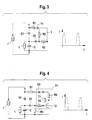
- the circuit is realized in that instead of the thyristor Th its equivalent circuit Th ' is used.
- This circuit can be less expensive than using a thyristor.
- the one described Thyristor function is through the diode D2, two Transistors T1, T2 and the resistor R4 reached.
- the diode D2 is important if the ideal only current source delivering positive current half-waves in one real, fed by the sinusoidal mains voltage Power source in combination with a high impedance consists. The reason for this is the low emitter-base reverse voltage usual transistors, which are not in the Are able to block the reverse voltage. For the Resistor R1 applies to what has been said above.
- the voltage U1 (target voltage range) is in the example about 24 V; the maximum voltage value U2 'of the voltage U2 is approximately 26 V.
- the load L is equal to Voltage U1 fed from the smoothing capacitor C as this is common for one-way rectification.
- FIG. A further exemplary embodiment is shown in FIG. where multiple loads from the AC power source J L, L1 ', L' 'are supplied.
- the load is a diode D1, D1 ', D1' 'in series and a smoothing capacitor C, C ', C' 'connected in parallel.
- the smoothing capacitors C, C ' are the positive current half-waves and the Smoothing capacitor C '' becomes the negative Current half-waves of the AC power source J supplied.
- everyone Series connection of smoothing capacitors and diodes is a bypass 1.1 ', 1' 'with switches 2.2', 2 '' connected in parallel, with each of the switches one Control 3,3 ', 3' 'is assigned.
- the realization can here also with the one described above Thyristor circuit or thyristor equivalent circuit respectively.
Landscapes
- Engineering & Computer Science (AREA)
- Power Engineering (AREA)
- Rectifiers (AREA)
- Bidet-Like Cleaning Device And Other Flush Toilet Accessories (AREA)
- Electrophonic Musical Instruments (AREA)
- Emergency Protection Circuit Devices (AREA)
Abstract
Description
Claims (10)
- Schaltung zur Stabilisierung der Spannung an einer von einer Wechselstromquelle gespeisten Last, wobei parallel zur Last ein Glättungskondensator und in Reihe zur Last eine Diode geschaltet sind und den Glättungskondensator die Stromhalbwellen der einen oder anderen Polarität der Wechselstromquelle auf einen Sollspannungsbereich der Last laden,
dadurch gekennzeichnet,
dass parallel zur Reihenschaltung der Last(L) und der Diode(D1) ein Bypass(1) geschaltet ist, in dem ein Schalter(2) liegt, und dass der Schalter(2) bei überschreiten der Sollspannung der Last(L) schließt, wobei die Diode(D1) die Entladung des Glättungskondensators(C) über den Bypass(1) verhindert. - Schaltung nach Anspruch 1,
dadurch gekennzeichnet,
dass der Schalter(2) bei Unterschreiten des Sollspannungsbereichs und/oder beim Nulldurchgang der Stromhalbwelle öffnet. - Schaltung nach Anspruch 1 oder 2,
dadurch gekennzeichnet,
dass im Bypass(1) ein Bauelement mit Diodenfunktion (D2, Th) angeordnet ist, wobei die Polung bezogen auf die Stromhalbwelle ebenso wie die Polung der Diode(D1) ist. - Schaltung nach Anspruch 3,
dadurch gekennzeichnet,
dass das Bauelement mit Diodenfunktion eine Diode(D2) ist. - Schaltung nach Anspruch 3,
dadurch gekennzeichnet.
dass der Schalter(2) und das Bauelement mit Diodenfunktion von einem Thyristor(Th) gebildet ist. - Schaltung nach einem der vorhergehenden Ansprüche 1 bis 4,
dadurch gekennzeichnet.
daß der Schalter(2) und das Bauelement mit Diodenfunktion von einer Thyristor-Ersatzschaltung(Th') gebildet ist. - Schaltung nach einem der vorhergehenden Ansprüche,
dadurch gekennzeichnet,
dass im Bypass(1) ein Widerstand(R1) zur Strombegrenzung angeordnet ist. - Schaltung nach Anspruch 7,
dadurch gekennzeichnet,
dass der Widerstand(R1) wesentlich kleiner als der ohmsche Innenwiderstand der Last(L) ist. - Schaltung nach einem der vorhergehenden Ansprüche 5 bis 8,
dadurch gekennzeichnet,
dass am Gate des Thyristors(Th) oder dessen Ersatzschaltung(Th') eine Zenerdiode(Z2) liegt, die bei der Sollspannung leitend wird und den Thyristor(Th) zündet oder dessen Ersatzschaltung(Th') leitend schaltet. - Schaltung nach einem der vorhergehenden Ansprüche,
dadurch gekennzeichnet,
dass die Wechselstromquelle(J) ein Kondensatornetzteil oder ein Widerstandsnetzteil ist, das an das Wechselspannungsnetz(N) anschließbar ist.
Applications Claiming Priority (2)
| Application Number | Priority Date | Filing Date | Title |
|---|---|---|---|
| DE10001711A DE10001711A1 (de) | 2000-01-18 | 2000-01-18 | Spannungsstabilisierungsschaltung an einer wechselstromgespeisten Last |
| DE10001711 | 2000-01-18 |
Publications (3)
| Publication Number | Publication Date |
|---|---|
| EP1119096A2 true EP1119096A2 (de) | 2001-07-25 |
| EP1119096A3 EP1119096A3 (de) | 2002-01-23 |
| EP1119096B1 EP1119096B1 (de) | 2003-07-09 |
Family
ID=7627757
Family Applications (1)
| Application Number | Title | Priority Date | Filing Date |
|---|---|---|---|
| EP01100797A Expired - Lifetime EP1119096B1 (de) | 2000-01-18 | 2001-01-15 | Spannungsstabilisierungsschaltung an einer wechselstromgespeisten Last |
Country Status (3)
| Country | Link |
|---|---|
| EP (1) | EP1119096B1 (de) |
| AT (1) | ATE244952T1 (de) |
| DE (2) | DE10001711A1 (de) |
Cited By (2)
| Publication number | Priority date | Publication date | Assignee | Title |
|---|---|---|---|---|
| EP2071425A1 (de) * | 2006-09-26 | 2009-06-17 | Tai-Her Yang | Schaltungseinrichtung mit Fähigkeit zur vollen Spannungsaktivierung, Spannungsteilerbetrieb und verzögertem Schalten |
| AU2008201386B2 (en) * | 2006-09-26 | 2013-08-29 | Tai-Her Yang | Circuit installation capable of full voltage activation, division voltage operation and delayed breaking |
Families Citing this family (2)
| Publication number | Priority date | Publication date | Assignee | Title |
|---|---|---|---|---|
| DE102009033385B4 (de) | 2009-07-16 | 2018-09-20 | Diehl Ako Stiftung & Co. Kg | Netzteil-Schaltungsanordnung und Verfahren zum Betreiben einer Netzteil-Schaltungsanordnung |
| DE102016009769A1 (de) | 2016-08-02 | 2018-02-08 | Theben Ag | Schaltungsanordnung |
Family Cites Families (3)
| Publication number | Priority date | Publication date | Assignee | Title |
|---|---|---|---|---|
| JPH0750982B2 (ja) * | 1989-04-11 | 1995-05-31 | 富士電気化学株式会社 | 電源装置 |
| JPH08140354A (ja) * | 1994-11-10 | 1996-05-31 | Tamura Seisakusho Co Ltd | 昇圧型アクティブフィルタの突入電流防止回路 |
| JPH11341809A (ja) * | 1998-05-27 | 1999-12-10 | Toshiba Corp | 電源回路 |
-
2000
- 2000-01-18 DE DE10001711A patent/DE10001711A1/de not_active Withdrawn
-
2001
- 2001-01-15 AT AT01100797T patent/ATE244952T1/de not_active IP Right Cessation
- 2001-01-15 DE DE50100352T patent/DE50100352D1/de not_active Expired - Fee Related
- 2001-01-15 EP EP01100797A patent/EP1119096B1/de not_active Expired - Lifetime
Cited By (2)
| Publication number | Priority date | Publication date | Assignee | Title |
|---|---|---|---|---|
| EP2071425A1 (de) * | 2006-09-26 | 2009-06-17 | Tai-Her Yang | Schaltungseinrichtung mit Fähigkeit zur vollen Spannungsaktivierung, Spannungsteilerbetrieb und verzögertem Schalten |
| AU2008201386B2 (en) * | 2006-09-26 | 2013-08-29 | Tai-Her Yang | Circuit installation capable of full voltage activation, division voltage operation and delayed breaking |
Also Published As
| Publication number | Publication date |
|---|---|
| DE50100352D1 (de) | 2003-08-14 |
| DE10001711A1 (de) | 2001-07-19 |
| EP1119096A3 (de) | 2002-01-23 |
| ATE244952T1 (de) | 2003-07-15 |
| EP1119096B1 (de) | 2003-07-09 |
Similar Documents
| Publication | Publication Date | Title |
|---|---|---|
| DE102006029475B4 (de) | Effiziente Einschaltstrom-Begrenzungsschaltung mit bidirektionellen Doppelgate-HEMT-Bauteilen | |
| DE19545154C2 (de) | Stromversorgungseinrichtung | |
| DE102013002266A1 (de) | Bootstrap-Schaltungsanordnung für einen IGBT | |
| DE60124760T2 (de) | Hybride elektrische schalteinrichtung | |
| WO2014075116A2 (de) | Konverter-modul für ein phasendimmen von leds | |
| DE602004002391T2 (de) | Generator für lichtbogenschweissvorrichtung mit hochleistungsfaktor | |
| EP1467474A2 (de) | Schnittstellenschaltung zum Betrieb von kapazitiven Lasten | |
| DE2634667A1 (de) | Leistungssteller | |
| EP1119096B1 (de) | Spannungsstabilisierungsschaltung an einer wechselstromgespeisten Last | |
| DE3504803C2 (de) | ||
| EP2826126A1 (de) | Leistungselektronische anordnung mit symmetrierung eines spannungsknotens im zwischenkreis | |
| DE69714754T2 (de) | Elektrische leistungssteuerung mit getakteter leistungsversorgungsschaltung | |
| DE2801844A1 (de) | Generatoraggregat | |
| DE2315497A1 (de) | Helligkeitssteuerschaltung fuer gasentladungslampen | |
| DE1805247A1 (de) | Stromversorgungsanlage | |
| CH650109A5 (en) | Method for operating a power capacitor for reactive-current compensation | |
| DE3317617A1 (de) | Kapazitive vorschalteinrichtung fuer niederspannungs-gluehlampe | |
| DE4130770C2 (de) | Verlustarme schaltungsanordnung zur ansteuerung eines aus dem wechselstromnetz gespeisten niedervolt-relais | |
| DE19841972A1 (de) | Getakteter Shuntregler | |
| DE1538538A1 (de) | Schaltungsanordnung fuer Abblendregler | |
| DE2745586C2 (de) | ||
| DE2647371A1 (de) | Steuerschaltung mit vergroesserter impedanz zur regelung der abgabeleistung von entladungslampen | |
| DE2647371C (de) | Schaltungsanordnung zum Betrieb von Entladungslampen in zwei Leistungsstufen | |
| EP1560675B1 (de) | Netzstromregelung für eine vielpunkt-widerstandsschweissmaschine mit einem aufladbaren energiespeicher | |
| DE3041840A1 (de) | Zweidraht-speiseschaltung |
Legal Events
| Date | Code | Title | Description |
|---|---|---|---|
| PUAI | Public reference made under article 153(3) epc to a published international application that has entered the european phase |
Free format text: ORIGINAL CODE: 0009012 |
|
| AK | Designated contracting states |
Kind code of ref document: A2 Designated state(s): AT BE CH CY DE DK ES FI FR GB GR IE IT LI LU MC NL PT SE TR |
|
| AX | Request for extension of the european patent |
Free format text: AL;LT;LV;MK;RO;SI |
|
| RIN1 | Information on inventor provided before grant (corrected) |
Inventor name: MANGOLD, HARALD |
|
| PUAL | Search report despatched |
Free format text: ORIGINAL CODE: 0009013 |
|
| AK | Designated contracting states |
Kind code of ref document: A3 Designated state(s): AT BE CH CY DE DK ES FI FR GB GR IE IT LI LU MC NL PT SE TR |
|
| AX | Request for extension of the european patent |
Free format text: AL;LT;LV;MK;RO;SI |
|
| 17P | Request for examination filed |
Effective date: 20020214 |
|
| AKX | Designation fees paid |
Free format text: AT BE CH CY DE DK ES FI FR GB GR IE IT LI LU MC NL PT SE TR |
|
| 17Q | First examination report despatched |
Effective date: 20020617 |
|
| GRAH | Despatch of communication of intention to grant a patent |
Free format text: ORIGINAL CODE: EPIDOS IGRA |
|
| GRAH | Despatch of communication of intention to grant a patent |
Free format text: ORIGINAL CODE: EPIDOS IGRA |
|
| GRAA | (expected) grant |
Free format text: ORIGINAL CODE: 0009210 |
|
| AK | Designated contracting states |
Designated state(s): AT BE CH CY DE DK ES FI FR GB GR IE IT LI LU MC NL PT SE TR |
|
| PG25 | Lapsed in a contracting state [announced via postgrant information from national office to epo] |
Ref country code: IT Free format text: LAPSE BECAUSE OF FAILURE TO SUBMIT A TRANSLATION OF THE DESCRIPTION OR TO PAY THE FEE WITHIN THE PRESCRIBED TIME-LIMIT;WARNING: LAPSES OF ITALIAN PATENTS WITH EFFECTIVE DATE BEFORE 2007 MAY HAVE OCCURRED AT ANY TIME BEFORE 2007. THE CORRECT EFFECTIVE DATE MAY BE DIFFERENT FROM THE ONE RECORDED. Effective date: 20030709 Ref country code: FR Free format text: LAPSE BECAUSE OF FAILURE TO SUBMIT A TRANSLATION OF THE DESCRIPTION OR TO PAY THE FEE WITHIN THE PRESCRIBED TIME-LIMIT Effective date: 20030709 Ref country code: IE Free format text: LAPSE BECAUSE OF FAILURE TO SUBMIT A TRANSLATION OF THE DESCRIPTION OR TO PAY THE FEE WITHIN THE PRESCRIBED TIME-LIMIT Effective date: 20030709 Ref country code: GB Free format text: LAPSE BECAUSE OF FAILURE TO SUBMIT A TRANSLATION OF THE DESCRIPTION OR TO PAY THE FEE WITHIN THE PRESCRIBED TIME-LIMIT Effective date: 20030709 Ref country code: FI Free format text: LAPSE BECAUSE OF FAILURE TO SUBMIT A TRANSLATION OF THE DESCRIPTION OR TO PAY THE FEE WITHIN THE PRESCRIBED TIME-LIMIT Effective date: 20030709 Ref country code: TR Free format text: LAPSE BECAUSE OF FAILURE TO SUBMIT A TRANSLATION OF THE DESCRIPTION OR TO PAY THE FEE WITHIN THE PRESCRIBED TIME-LIMIT Effective date: 20030709 Ref country code: CY Free format text: LAPSE BECAUSE OF FAILURE TO SUBMIT A TRANSLATION OF THE DESCRIPTION OR TO PAY THE FEE WITHIN THE PRESCRIBED TIME-LIMIT Effective date: 20030709 Ref country code: NL Free format text: LAPSE BECAUSE OF FAILURE TO SUBMIT A TRANSLATION OF THE DESCRIPTION OR TO PAY THE FEE WITHIN THE PRESCRIBED TIME-LIMIT Effective date: 20030709 |
|
| REG | Reference to a national code |
Ref country code: GB Ref legal event code: FG4D Free format text: NOT ENGLISH |
|
| REG | Reference to a national code |
Ref country code: CH Ref legal event code: EP |
|
| REF | Corresponds to: |
Ref document number: 50100352 Country of ref document: DE Date of ref document: 20030814 Kind code of ref document: P |
|
| REG | Reference to a national code |
Ref country code: IE Ref legal event code: FG4D Free format text: GERMAN |
|
| PG25 | Lapsed in a contracting state [announced via postgrant information from national office to epo] |
Ref country code: DK Free format text: LAPSE BECAUSE OF FAILURE TO SUBMIT A TRANSLATION OF THE DESCRIPTION OR TO PAY THE FEE WITHIN THE PRESCRIBED TIME-LIMIT Effective date: 20031009 Ref country code: SE Free format text: LAPSE BECAUSE OF FAILURE TO SUBMIT A TRANSLATION OF THE DESCRIPTION OR TO PAY THE FEE WITHIN THE PRESCRIBED TIME-LIMIT Effective date: 20031009 Ref country code: GR Free format text: LAPSE BECAUSE OF FAILURE TO SUBMIT A TRANSLATION OF THE DESCRIPTION OR TO PAY THE FEE WITHIN THE PRESCRIBED TIME-LIMIT Effective date: 20031009 |
|
| PG25 | Lapsed in a contracting state [announced via postgrant information from national office to epo] |
Ref country code: ES Free format text: LAPSE BECAUSE OF FAILURE TO SUBMIT A TRANSLATION OF THE DESCRIPTION OR TO PAY THE FEE WITHIN THE PRESCRIBED TIME-LIMIT Effective date: 20031020 |
|
| REG | Reference to a national code |
Ref country code: CH Ref legal event code: NV Representative=s name: A. BRAUN, BRAUN, HERITIER, ESCHMANN AG PATENTANWAE |
|
| NLV1 | Nl: lapsed or annulled due to failure to fulfill the requirements of art. 29p and 29m of the patents act | ||
| PG25 | Lapsed in a contracting state [announced via postgrant information from national office to epo] |
Ref country code: PT Free format text: LAPSE BECAUSE OF FAILURE TO SUBMIT A TRANSLATION OF THE DESCRIPTION OR TO PAY THE FEE WITHIN THE PRESCRIBED TIME-LIMIT Effective date: 20031209 |
|
| GBV | Gb: ep patent (uk) treated as always having been void in accordance with gb section 77(7)/1977 [no translation filed] |
Effective date: 20030709 |
|
| PG25 | Lapsed in a contracting state [announced via postgrant information from national office to epo] |
Ref country code: LU Free format text: LAPSE BECAUSE OF NON-PAYMENT OF DUE FEES Effective date: 20040115 |
|
| PG25 | Lapsed in a contracting state [announced via postgrant information from national office to epo] |
Ref country code: BE Free format text: LAPSE BECAUSE OF NON-PAYMENT OF DUE FEES Effective date: 20040131 Ref country code: MC Free format text: LAPSE BECAUSE OF NON-PAYMENT OF DUE FEES Effective date: 20040131 |
|
| REG | Reference to a national code |
Ref country code: IE Ref legal event code: FD4D |
|
| PLBE | No opposition filed within time limit |
Free format text: ORIGINAL CODE: 0009261 |
|
| STAA | Information on the status of an ep patent application or granted ep patent |
Free format text: STATUS: NO OPPOSITION FILED WITHIN TIME LIMIT |
|
| 26N | No opposition filed |
Effective date: 20040414 |
|
| EN | Fr: translation not filed | ||
| BERE | Be: lapsed |
Owner name: *DIEHL AKO STIFTUNG & CO. K.G. Effective date: 20040131 |
|
| PGFP | Annual fee paid to national office [announced via postgrant information from national office to epo] |
Ref country code: CH Payment date: 20080131 Year of fee payment: 8 |
|
| PGFP | Annual fee paid to national office [announced via postgrant information from national office to epo] |
Ref country code: DE Payment date: 20080319 Year of fee payment: 8 |
|
| REG | Reference to a national code |
Ref country code: CH Ref legal event code: PFA Owner name: DIEHL AKO STIFTUNG & CO. KG Free format text: DIEHL AKO STIFTUNG & CO. KG#PFANNERSTRASSE 75#88239 WANGEN (DE) -TRANSFER TO- DIEHL AKO STIFTUNG & CO. KG#PFANNERSTRASSE 75#88239 WANGEN (DE) |
|
| PGFP | Annual fee paid to national office [announced via postgrant information from national office to epo] |
Ref country code: AT Payment date: 20081222 Year of fee payment: 9 |
|
| REG | Reference to a national code |
Ref country code: CH Ref legal event code: PL |
|
| PG25 | Lapsed in a contracting state [announced via postgrant information from national office to epo] |
Ref country code: LI Free format text: LAPSE BECAUSE OF NON-PAYMENT OF DUE FEES Effective date: 20090131 Ref country code: CH Free format text: LAPSE BECAUSE OF NON-PAYMENT OF DUE FEES Effective date: 20090131 Ref country code: DE Free format text: LAPSE BECAUSE OF NON-PAYMENT OF DUE FEES Effective date: 20090801 |
|
| PG25 | Lapsed in a contracting state [announced via postgrant information from national office to epo] |
Ref country code: AT Free format text: LAPSE BECAUSE OF NON-PAYMENT OF DUE FEES Effective date: 20100115 |