EP1119016A2 - Gas shower unit for semiconductor manufacturing apparatus and semiconductor manufacturing apparatus - Google Patents
Gas shower unit for semiconductor manufacturing apparatus and semiconductor manufacturing apparatus Download PDFInfo
- Publication number
- EP1119016A2 EP1119016A2 EP01300473A EP01300473A EP1119016A2 EP 1119016 A2 EP1119016 A2 EP 1119016A2 EP 01300473 A EP01300473 A EP 01300473A EP 01300473 A EP01300473 A EP 01300473A EP 1119016 A2 EP1119016 A2 EP 1119016A2
- Authority
- EP
- European Patent Office
- Prior art keywords
- shower unit
- gas shower
- unit according
- base material
- gas
- Prior art date
- Legal status (The legal status is an assumption and is not a legal conclusion. Google has not performed a legal analysis and makes no representation as to the accuracy of the status listed.)
- Granted
Links
Images




Classifications
-
- C—CHEMISTRY; METALLURGY
- C23—COATING METALLIC MATERIAL; COATING MATERIAL WITH METALLIC MATERIAL; CHEMICAL SURFACE TREATMENT; DIFFUSION TREATMENT OF METALLIC MATERIAL; COATING BY VACUUM EVAPORATION, BY SPUTTERING, BY ION IMPLANTATION OR BY CHEMICAL VAPOUR DEPOSITION, IN GENERAL; INHIBITING CORROSION OF METALLIC MATERIAL OR INCRUSTATION IN GENERAL
- C23C—COATING METALLIC MATERIAL; COATING MATERIAL WITH METALLIC MATERIAL; SURFACE TREATMENT OF METALLIC MATERIAL BY DIFFUSION INTO THE SURFACE, BY CHEMICAL CONVERSION OR SUBSTITUTION; COATING BY VACUUM EVAPORATION, BY SPUTTERING, BY ION IMPLANTATION OR BY CHEMICAL VAPOUR DEPOSITION, IN GENERAL
- C23C16/00—Chemical coating by decomposition of gaseous compounds, without leaving reaction products of surface material in the coating, i.e. chemical vapour deposition [CVD] processes
- C23C16/44—Chemical coating by decomposition of gaseous compounds, without leaving reaction products of surface material in the coating, i.e. chemical vapour deposition [CVD] processes characterised by the method of coating
- C23C16/455—Chemical coating by decomposition of gaseous compounds, without leaving reaction products of surface material in the coating, i.e. chemical vapour deposition [CVD] processes characterised by the method of coating characterised by the method used for introducing gases into reaction chamber or for modifying gas flows in reaction chamber
- C23C16/45563—Gas nozzles
- C23C16/45565—Shower nozzles
-
- H—ELECTRICITY
- H10—SEMICONDUCTOR DEVICES; ELECTRIC SOLID-STATE DEVICES NOT OTHERWISE PROVIDED FOR
- H10P—GENERIC PROCESSES OR APPARATUS FOR THE MANUFACTURE OR TREATMENT OF DEVICES COVERED BY CLASS H10
- H10P95/00—Generic processes or apparatus for manufacture or treatments not covered by the other groups of this subclass
-
- C—CHEMISTRY; METALLURGY
- C23—COATING METALLIC MATERIAL; COATING MATERIAL WITH METALLIC MATERIAL; CHEMICAL SURFACE TREATMENT; DIFFUSION TREATMENT OF METALLIC MATERIAL; COATING BY VACUUM EVAPORATION, BY SPUTTERING, BY ION IMPLANTATION OR BY CHEMICAL VAPOUR DEPOSITION, IN GENERAL; INHIBITING CORROSION OF METALLIC MATERIAL OR INCRUSTATION IN GENERAL
- C23C—COATING METALLIC MATERIAL; COATING MATERIAL WITH METALLIC MATERIAL; SURFACE TREATMENT OF METALLIC MATERIAL BY DIFFUSION INTO THE SURFACE, BY CHEMICAL CONVERSION OR SUBSTITUTION; COATING BY VACUUM EVAPORATION, BY SPUTTERING, BY ION IMPLANTATION OR BY CHEMICAL VAPOUR DEPOSITION, IN GENERAL
- C23C16/00—Chemical coating by decomposition of gaseous compounds, without leaving reaction products of surface material in the coating, i.e. chemical vapour deposition [CVD] processes
- C23C16/44—Chemical coating by decomposition of gaseous compounds, without leaving reaction products of surface material in the coating, i.e. chemical vapour deposition [CVD] processes characterised by the method of coating
- C23C16/455—Chemical coating by decomposition of gaseous compounds, without leaving reaction products of surface material in the coating, i.e. chemical vapour deposition [CVD] processes characterised by the method of coating characterised by the method used for introducing gases into reaction chamber or for modifying gas flows in reaction chamber
-
- H—ELECTRICITY
- H01—ELECTRIC ELEMENTS
- H01J—ELECTRIC DISCHARGE TUBES OR DISCHARGE LAMPS
- H01J37/00—Discharge tubes with provision for introducing objects or material to be exposed to the discharge, e.g. for the purpose of examination or processing thereof
- H01J37/32—Gas-filled discharge tubes
- H01J37/32431—Constructional details of the reactor
- H01J37/3244—Gas supply means
Definitions
- the present invention relates to a gas shower unit for a semiconductor manufacturing apparatus.
- the invention relates to a gas shower unit used in a semiconductor manufacturing apparatus such as CVD apparatus, plasma CVD apparatus, etching apparatus and plasma etching apparatus for the purpose of uniformly supplying reactant gas to a semiconductor wafer.
- etching of a semiconductor wafer surface or depositing of a film thereon a method has been employed according to which gas for etching or for film deposition is supplied by means of batch processing to a large number of wafers held on racks, and then the wafers are heated as required from the outer periphery (hot wall method).
- a semiconductor wafer is placed on the surface of a holder made of ceramics or metal.
- the wafer is secured onto the holder surface statically, mechanically, or by applying voltage to an electrode provided in the holder so as to fasten the wafer by an electrostatic force.
- the surface temperature of the semiconductor wafer held on the holder is precisely controlled in order to adjust the film deposition rate or etching rate in the process of CVD (Chemical Vapor Deposition), plasma CVD, etching, plasma etching or the like.
- CVD Chemical Vapor Deposition
- plasma CVD plasma CVD
- etching plasma etching
- plasma etching plasma etching
- reactant gas is merely supplied through a pipe attached to a chamber of the semiconductor manufacturing apparatus, gas does not uniformly flow through respective regions where the gas is directly and indirectly supplied respectively. As a result, the reactant gas has different concentrations on the surface of a semiconductor wafer. Control accordingly becomes difficult for realizing uniform etching or film deposition on the surface of the semiconductor wafer.
- a method is employed according to which a gas shower unit is positioned directly above the semiconductor wafer, the shower unit being formed of a sheetlike base material with a large number of through holes formed therein. This method enables gas to blow out as if from a showerhead, and consequently the gas concentration can be made as constant as possible on the semiconductor wafer surface.
- the temperature at which the gas is caused to react is different depending on the type of reactant gas. Approximately, the temperature is 100 to 400°C for high-temperature etching, 200 to 500°C for plasma CVD and 400 to 800°C for CVD.
- the wafer holder has a heater therein to directly heat a wafer and adjust temperature to the one required for reaction. If a reactant gas at room temperature is directly supplied from the gas shower unit, the reactant gas is suddenly heated on the wafer and accordingly the wafer temperature is decreased. Therefore, it is difficult to make the gas temperature constant especially over the surface of a large-area wafer and the reaction rate varies depending on the location on the wafer, so that a film having a uniform thickness is difficult to produce.
- a method of preliminary heating a reactant gas may be employed according to which the reactant gas is supplied into a chamber from piping provided outside a semiconductor manufacturing apparatus, and the gas is heated by a heater and then passed through a gas shower unit.
- a heater may be provided in a gas shower unit. If the gas shower unit having a heater therein is produced by providing a heater coil or wire between ceramics compact pieces and hot-press sintering them, the thickness of a base material of the gas shower unit is 10 mm or more because the heater coil embedded within the base material has an outer diameter of approximately 3 to 6 mm. As a result, through holes are likely to clog. Further, since the through holes should be formed not to touch the heater coil, there is a limitation on locations where the through holes are to be made. In this case, in many regions, the interval between through holes is 3 to 6 mm or more. In addition, if the gas shower unit has a greater thickness due to an embedded coil, the through holes are accordingly longer and thus likely to clog as described above.
- a further method employed for ensuring uniform heating on a wafer where reaction occurs is that a gas shower unit is warmed by heat radiated from a wafer holder which has a heater therein and is located under a wafer, and after the gas shower unit is warmed to a predetermined temperature, gas is supplied therefrom.
- a film is stacked not only on a wafer as a product but also on the gas shower unit, wafer holder and chamber.
- thermal stress causes peeling of the film, which generates particles attached onto the product wafer, and accordingly defect occurs. Therefore, the surfaces of components within the chamber should be cleaned frequently.
- the optimum temperature for film deposition and that for cleaning are different.
- such a gas as ClF3, NF3 or the like is used for cleaning. Since this type of gas would have too great etching power if used at the film deposition temperature, temperature in cleaning should be made lower than the film deposition temperature so as not to excessively damage the surfaces of the gas shower unit, wafer holder and chamber.
- the temperature should be changed in the course from film deposition (high temperature), cleaning (low temperature), then to film deposition (high temperature) and so on.
- the gas shower unit having no heater therein is heated only by heat radiated from the heater located below and accordingly takes a considerable time to reach a predetermined temperature.
- the incorporated cleaning process constitutes a main factor in decrease of throughput in wafer processing.
- One object of the present invention is to provide a gas shower unit for a semiconductor manufacturing apparatus and to provide a semiconductor manufacturing apparatus including therein the gas shower unit, to enable reaction to occur uniformly within a chamber of the semiconductor manufacturing apparatus such as CVD apparatus, plasma CVD apparatus, etching apparatus and the like while overcoming the problems above.
- Another object of the invention is to provide a gas shower unit for a semiconductor manufacturing apparatus and to provide a semiconductor manufacturing apparatus including therein the gas shower unit, in which clogging of through holes hardly occurs in the gas shower unit of a thin type and in which a cleaning step can readily be done even when unnecessary films which could cause clogging or produce particles are deposited on the surfaces of components within a chamber of the semiconductor manufacturing apparatus, thus increasing throughput in wafer processing.
- a gas shower unit for a semiconductor manufacturing apparatus has a base material of 5 mm or less in thickness, and includes a sintered ceramics base material having a plurality of through holes and a conductive layer formed in the sintered ceramics base material.
- a desirable gas shower unit for decreasing the frequency of cleaning steps has through holes which are not clogged for at least 24 hours.
- a gas shower unit can be employed which includes a base material of 5 mm or less in thickness with through holes each of a normal diameter (at least 0.01 mm) in order to prevent the through holes from being clogged for at least 24 hours. Accordingly, if the gas shower unit according to the present invention is employed, through holes hardly clog in the thin gas shower unit, and preliminary heating, which could cause clogging of the through holes, is unnecessary.
- the heater can be included as the conductive layer in the gas shower unit so as to smoothly increase temperature, from a lower one at which cleaning is done for removing a deposited film attached to chamber components that generates particles, to a higher one at which a film is deposited on a wafer, and accordingly throughput in wafer processing can be enhanced.
- a desirable time period required to increase and decrease temperature is one hour or less in total. Including of the heater can reduce the time for increasing the temperature, and forming of a gas shower unit into a thin shape can reduce the time for decreasing the temperature.
- the gas shower unit according to the present invention includes a conductive layer where a heater circuit pattern is formed. Accordingly, reactant gas is preliminary heated when it passes through holes of the gas shower unit so that reaction uniformly occurs in a chamber for a semiconductor manufacturing apparatus. Occurrence of through hole clogging as well as generation of particles can thus be avoided.
- the conductive layer of the gas shower unit according to the present invention includes a conductive layer in which an electrode for generating plasma is formed.
- a conductive layer in which an electrode for generating plasma is formed.
- the sintered ceramics base material of the gas shower unit according to the present invention has at least 0.1 through holes per square centimeter each having a diameter of 0.01 mm or more. More preferably, the sintered ceramics base material has at least 0.5 through holes per square centimeter each having a diameter of 0.01 mm or more.
- the dimension and density of the above numerical values of through holes enables reactant gas to be supplied uniformly onto a semiconductor wafer within a chamber of a semiconductor manufacturing apparatus. Accordingly, temperature distribution over the semiconductor wafer can be made more uniform.
- Ceramics used for the base material constituting the gas shower unit according to the present invention preferably includes any one of aluminum nitride, aluminum oxide, silicon nitride and aluminum oxynitride.
- the aluminum nitride is most preferred because of its heat conductivity and corrosion resistance.
- Such a ceramics material provides the base material of the gas shower unit with heat resistance as well as corrosion resistance against corrosive gas containing halogen, for example, used as a reactant gas.
- the sintered ceramics base material includes a first sintered ceramics piece and a second sintered ceramics piece and the conductive layer is preferably formed on a surface of the first sintered ceramics piece.
- the gas shower unit of the present invention preferably includes a joint layer interposed between the surface of the first sintered ceramics piece having the conductive layer formed thereon and the second sintered ceramics piece, for coupling the first and second sintered ceramics pieces.
- the gas shower unit of the present invention may be structured by forming a conductive layer on one surface or both surfaces of a sintered ceramics base material and forming a protective layer to cover a surface of the conductive layer.
- a gas shower unit including a heater circuit therein may have a structure in which only one sintered ceramics piece is used as the sintered ceramics base material, a conductive layer is formed as a heater circuit pattern on one surface of the sintered ceramics piece, and a surface of the conductive layer is covered with a protective layer having a high corrosion resistance, preferably a protective layer formed of nonoxide ceramics in order to protect the conductive layer from corrosive gas such as halogen and the like.
- a gas shower unit including therein a heater circuit and a plasma upper electrode may have a structure in which only one sintered ceramics piece is used as the sintered ceramics base material, a conductive layer is formed as a heater circuit pattern on one surface of the sintered ceramics piece, a conductive layer is formed as a plasma upper electrode on the other surface of the sintered ceramics piece, and the surfaces of the conductive layers formed respectively on both surfaces of the sintered ceramics piece are covered with a protective layer having a high corrosion resistance, preferably a protective layer formed of nonoxide ceramics in order to protect the conductive layers from corrosive gas such as halogen and the like.
- a protective layer having a high corrosion resistance preferably a protective layer formed of nonoxide ceramics in order to protect the conductive layers from corrosive gas such as halogen and the like.
- the joint layer or protective layer preferably includes glass. If the gas shower unit is used at a high temperature with a high voltage applied thereto, the joint layer or protective layer more preferably includes nonoxide ceramics in terms of heat resistance, corrosion resistance and voltage resistance. In this case, the nonoxide ceramics preferably includes at least 50 % by mass of any of aluminum nitride and silicon nitride.
- the joint layer above is preferably a glass layer having a coefficient of thermal expansion of at least 3.0 ⁇ 10 -6 /°C and at most 8.0 ⁇ 10 -6 /°C.
- a glass layer as the joint layer enables the thermal expansion coefficient of the joint layer to be almost equal to that of the sintered ceramics piece. Consequently, thermal stress generated in joining, or heating and cooling of the gas shower unit can be decreased.
- the protective layer As the protective layer above, a glass having corrosion resistance as high as possible is preferably used.
- the protective layer is preferably a glass layer having a thermal expansion coefficient of at least 3.0 ⁇ 10 -6 /°C and at most 8.0 ⁇ 10 - 6 /°C.
- the target time for heating the gas shower unit from room temperature to 600°C is 30 minutes or less. If the thermal expansion coefficient falls in the range above, this target can be achieved.
- the joint layer including glass preferably includes oxide containing ytterbium (Yb), neodymium (Nd) and calcium (Ca) or includes a compound which generates oxide containing ytterbium (Yb), neodymium (Nd) and calcium (Ca) by being heated.
- the joint layer including glass preferably includes oxide containing yttrium (Y) and aluminum (Al) or includes a compound which generates oxide containing yttrium (Y) and aluminum (Al) by being heated.
- nonoxide ceramics is used as a material for the joint layer or protective layer, in consideration of thermal stress, nonoxide ceramics having a thermal expansion coefficient of at least 3.0 ⁇ 10 -6 /°C and at most 6.0 ⁇ 10 -6 /°C is preferably used.
- the conductive layer in the gas shower unit according to the present invention includes at least one of tungsten, molybdenum, silver, palladium, platinum, nickel and chromium.
- the conductive layer in the gas shower unit according to the present invention is formed along a plane within the sintered ceramics base material.
- the gas shower unit preferably includes an external connection terminal which is formed along the same plane as that in the sintered ceramics base material to connect to the conductive layer and exposed from the sintered ceramics base material. It is accordingly possible to expose to reactant gas only the region of the sintered ceramics base material including the conductive layer therein and to locate the external connection terminal outside a chamber of a semiconductor manufacturing apparatus. Since the conductive layer included in the sintered ceramics base material and the external connection terminal coupled to the conductive layer are formed along the same plane, uniform heating of the gas shower unit as well as shortening of time period required for heating and cooling are possible. In other words, heating and cooling rates can be enhanced.
- the gas shower unit according to the invention further includes a temperature detection unit included in the sintered ceramics base material. Temperature distribution in the gas shower unit can thus be measured to control heating temperature of the gas shower unit.
- a semiconductor manufacturing apparatus includes therein the semiconductor manufacturing apparatus gas shower unit structured in the above-described manner.
- the semiconductor manufacturing apparatus is one selected from the group consisting of etching apparatus, CVD apparatus and plasma CVD apparatus.
- a gas shower unit used for a semiconductor manufacturing apparatus such as CVD apparatus, plasma CVD apparatus, high temperature etching apparatus and the like where heating should be done more uniformly because of increased outer diameter of a semiconductor wafer to be processed
- a structure having a heater function or a structure having both of the heater and plasma electrode functions Use of a gas shower unit having such a structure enables reactant gas to be heated uniformly, and accordingly enables film deposition or etching to be done uniformly on a semiconductor wafer surface.
- there is generated no unnecessary film on the surface of the base material of the gas shower unit and thus it is possible to prevent the concentration and flow rate of gas within a chamber from changing with time due to clogging of through holes. Further, it is possible to prevent particles from being generated resulting from peeling of a film attached to the surface of the base material of the gas shower unit.
- Fig. 1 illustrates one embodiment of a semiconductor manufacturing apparatus to which a gas shower unit according to the present invention is applicable.
- Fig. 2 illustrates another embodiment of the semiconductor manufacturing apparatus to which a gas shower unit according to the present invention is applicable.
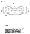
- Fig. 3 is a perspective view illustrating one embodiment of a gas shower unit according to the present invention.
- Fig. 4 shows a cross section of a gas shower unit including a heater function therein as one embodiment of the gas shower unit according to the present invention.
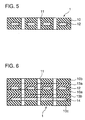
- Fig. 5 shows a cross sectional structure of a gas shower unit including a heater function therein as another embodiment of the gas shower unit according to the invention.
- Fig. 6 shows a cross section of a gas shower unit having both of heater and plasma electrode functions as a further embodiment of the gas shower unit according to the invention.
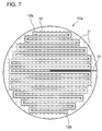
- Fig. 7 is a plan view of the gas shower unit according to the invention showing, as one embodiment of a base material of the gas shower unit, one surface where a heater circuit pattern is formed.
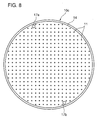
- Fig. 8 is a plan view of the gas shower unit according to the invention showing, as one embodiment of a base material of the gas shower unit, one surface where a plasma upper electrode is formed.
- Fig. 9 shows a cross section of a gas shower unit having a heater function therein as a further embodiment of the gas shower unit according to the invention.
- Fig. 10 shows a cross section of a gas shower unit having both of heater and plasma electrode functions as a further embodiment of the gas shower unit according to the invention.
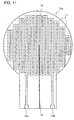
- Fig. 11 is a plan view of the gas shower unit according to the invention showing, as another embodiment of a base material of the gas shower unit, one surface where a heater circuit pattern is formed.
- Fig. 12 is a plan view of the gas shower unit according to the invention showing, as a further embodiment of a base material of the gas shower unit, one surface where a plasma upper electrode is formed.
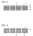
- Fig. 13 illustrates a cross section of a gas shower unit as an example for comparison with the present invention.
- Fig. 14 illustrates a cross section of a gas shower unit as another example for comparison with the present invention.
- Figs. 1 and 2 respectively show embodiments of a semiconductor manufacturing apparatus to which a gas shower unit of the present invention is applied.
- a semiconductor wafer 3 to be processed by means of film deposition or etching is placed in a chamber 101 of a CVD apparatus or an etching apparatus.
- Semiconductor wafer 3 is fixed onto a wafer holder 2.
- Wafer holder 2 is attached to a supporter 4.
- Wafer holder 2 includes an electrostatic chuck electrode 23 for securing semiconductor wafer 3 by an electrostatic force, and a heater circuit 21 for heating semiconductor wafer 3.
- a gas shower unit 1 is placed above semiconductor wafer 3.
- Gas shower unit 1 has a plurality of through holes 11 to pass reactant gas therethrough and includes therein a heater circuit pattern for heating the reactant gas.
- the heater circuit pattern is included in gas shower unit 1 in the form of a conductive layer.
- Reactant gas for film deposition or etching gas is introduced from a gas inlet 200 into chamber 101.
- the introduced gas passes through a plurality of through holes 11 to be supplied onto the surface of semiconductor wafer 3.
- a predetermined film deposition or etching is done on the surface of semiconductor wafer 3.
- a gas discharge outlet 300 is provided for discharging gas from the inside of chamber 101.
- a semiconductor wafer 3 to be processed by means of film deposition or etching is placed in a chamber 102 used for a plasma CVD apparatus or a plasma etching apparatus.
- Semiconductor wafer 3 is fixed onto a wafer holder 2.
- Wafer holder 2 is attached onto a supporter 4.
- Wafer holder 2 includes a heater circuit 21 for heating semiconductor wafer 3, a plasma lower electrode 22 for generating plasma in chamber 102, and an electrostatic chuck electrode 23 for generating an electrostatic force to secure semiconductor wafer 3.
- a gas shower unit 1 is placed above semiconductor wafer 3.
- Gas shower unit 1 has a plurality of through holes 11 for passing reactant gas therethrough, and includes therein a plasma upper electrode opposite plasma lower electrode 22 and a heater circuit pattern for heating the reactant gas.
- the heater circuit pattern and the plasma upper electrode are included in the form of conductive layer in gas shower unit 1.
- Gas for film deposition or etching gas is introduced from a gas inlet 200 into chamber 102, passing through holes 11 of gas shower unit 1 to be supplied onto the surface of semiconductor wafer 3. Plasma discharge occurs between the plasma upper electrode included in gas shower unit 1 and plasma lower electrode 22 included in wafer holder 2. By the gas plasma thus generated, a predetermined film deposition or etching is performed on the surface of semiconductor wafer 3.
- a gas discharge outlet 300 is provided for discharging gas from the inside of chamber 102.
- Fig. 3 is a perspective view illustrating one embodiment of the gas shower unit according to the present invention.
- a base material 10 of sintered ceramics hereinafter referred to as sintered ceramics base material 10
- sintered ceramics base material 10 includes therein a conductive layer where a heater circuit pattern 12 or a plasma upper electrode 14 is formed.
- Figs. 4 to 6, 9 and 10 respectively show cross sectional structures as respective embodiments of the gas shower unit according to the present invention.
- gas shower unit 1 has a structure in which two sintered ceramics base materials 10a and lOb are joined. On one surface of sintered ceramics base material 10a, heater circuit pattern 12 is formed. Between the one surface of sintered ceramics base material 10a where the heater circuit pattern 12 is formed and a surface of sintered ceramics base material lOb, a glass layer or nonoxide ceramics layer 13 is provided to join sintered ceramics base materials 10a and lOb. A plurality of through holes 11 are formed to pass through sintered ceramics base material 10a, glass layer or nonoxide ceramics layer 13, and sintered ceramics base material 10b. Heater circuit pattern 12 is formed to avoid through holes 11.
- gas shower unit 1 includes no glass layer or nonoxide ceramics layer as a joint layer.
- gas shower unit 1 includes therein heater circuit pattern 12 and plasma upper electrode 14 in the form of conductive layer.
- heater circuit pattern 12 is formed as a conductive layer.
- Sintered ceramics pieces 10a and 10b are joined by providing a glass layer or nonoxide ceramics layer 13a between the one surface of sintered ceramics piece 10a where heater circuit pattern 12 is formed and sintered ceramics piece 10b.
- plasma upper electrode 14 is formed as a conductive layer.
- gas shower unit 1 having the heater function and the plasma electrode is structured.
- gas shower unit 1 may include only one conductive layer serving both functions of a heater circuit pattern and a plasma upper electrode.
- the gas shower unit may be structured to include therein the plasma upper electrode only.
- Fig. 7 is a plan view showing one surface of sintered ceramics base material 10a where the heater circuit pattern is formed. As shown in Fig. 7, a plurality of fine through holes 11 are formed in one surface of sintered ceramics base material 10a. Heater circuit pattern 12 is formed in a zigzag following a certain pattern, avoiding contact with the locations of through holes 11. Circular connection terminals 12a and 12b are formed on both ends of heater circuit pattern 12 for connection to the outside. In addition, on the one surface of sintered ceramics base material 10a, a groove 15 is formed for insertion of a temperature sensor as a temperature detecting unit.
- Fig. 8 is a plan view showing one surface of a sintered ceramics base material where the plasma upper electrode is formed.
- a plurality of fine through holes 11 are formed in the one surface of sintered ceramics base material 10c such that the locations of through holes 11 match respective through holes of sintered ceramics base material 10a shown in Fig. 7.
- Two through holes 17a and 17b are formed to match, in location, connection terminals 12a and 12b respectively of the heater circuit pattern shown in Fig. 7.
- Plasma upper electrode 14 is formed on the one surface of sintered ceramics base material 10c to cover almost entire surface without blocking up openings of through holes 11.
- heater circuit pattern 12 is formed as a conductive layer on one surface of sintered ceramics piece 10a.
- Nonoxide ceramics layer 13a is used to cover the one surface of sintered ceramics piece 10a where heater circuit pattern 12 is formed in order to form a protective layer for protecting the heater circuit pattern from corrosive gas such as halogen and the like.
- one sintered ceramics piece 10a may be used to construct gas shower unit 1 including therein heater circuit pattern 12 in the form of a conductive layer.
- heater circuit pattern 12 and plasma upper electrode 14 may be formed in the form of conductive layers respectively on one surface and the other surface of sintered ceramics piece 10a.
- nonoxide ceramics layers 13a and 13b covering the conductive layers respectively are used to form protective layers for protecting heater circuit pattern 12 and plasma upper electrode 14 as the conductive layers from corrosive gas such as halogen and the like.
- one sintered ceramics piece 10a may be used to construct gas shower unit 1 including therein heater circuit pattern 12 and plasma upper electrode 14 in the form of conductive layers.
- Fig. 11 is a plan view showing, as another embodiment, one surface of sintered ceramics base material 10a where a heater circuit pattern is formed.
- connection terminals 12a and 12b are formed along the same plane on the one surface of sintered ceramics base material 10a to be connected to heater circuit pattern 12.
- Connection terminals 12a and 12b extend to a side surface for connection to lines outside the chamber of the semiconductor manufacturing apparatus.
- a groove 15 also extends to the side surface of sintered ceramics base material 10a for inserting a temperature sensor therein from the outside of the chamber of the semiconductor manufacturing apparatus. Based on temperature measured by the temperature sensor, the temperature of the gas shower unit can be controlled by using a temperature adjustment module provided outside the semiconductor manufacturing apparatus.
- Fig. 12 is a plan view showing, as another embodiment, one surface of sintered ceramics base material 10c where a plasma upper electrode is formed. As shown in Fig. 12, a connection terminal 14a is formed along the same plane on the one surface of sintered ceramics base material 10c to be connected to plasma upper electrode 14. Connection terminal 14a extends to a side surface of sintered ceramics base material 10c for connection to lines outside the chamber of the semiconductor manufacturing apparatus.
- a sintered ceramics piece constituting a base material of the gas shower unit of the present invention can be manufactured by means of a conventional method. Specifically, a sintering agent is added to ceramics powder as required, a binder is further added if necessary, and then a compact piece of that powder mixture is sintered. Since ceramics has heat resistance as well as corrosion resistance against corrosive gas including halogen and the like, aluminum nitride, aluminum oxide, silicon nitride and aluminum oxynitride are preferred. Among them, aluminum nitride is most preferred because of its heat conductivity and corrosion resistance.
- any of well-known sheet forming methods such as doctor blade process, extrusion, press and the like is used.
- the compact piece is dried and then undergoes punching or cutting into a shape which allows the degree of shrinkage after sintering. Through holes may be made at this stage, or by machining after sintered pieces are joined.
- Binder is removed from the compact piece and thereafter the compact piece is sintered, preferably at a normal pressure.
- the surface of the sintered piece may be polished or the sintered piece may be cut if necessary.
- the sintered piece may directly be used as the base material of the gas shower unit.
- paste containing conductive material for example, refractory metal such as tungsten, molybdenum and the like or mixture thereof, or metal or alloy such as silver, silver-palladium, nickel-chromium and the like is applied by printing on the surface of the sintered piece and then baked.
- a joint element such as glass, nonoxide ceramics or the like is applied.
- the ceramics pieces overlaid on each other are accordingly joined. In this way, the gas shower unit can be manufactured having the sintered ceramics base material within which the conductive layer is included.
- the manufacturing method discussed above employs so-called post metalizing method according to which a conductive layer is formed by applying paste containing conductive material onto a sintered ceramics piece and then baking it.
- the co-fire method may be employed for providing within a sintered ceramics base material a conductive layer corresponding to a heater circuit pattern or plasma upper electrode.
- paste containing refractory metal such as tungsten, molybdenum and the like or mixture thereof is applied by printing onto a surface of a ceramics compact piece, another ceramics compact piece is overlaid thereon to bind them through thermal compression, the compact pieces are deprived of binder, and then sintering of the compact ceramics pieces and baking of the conductive paste are simultaneously performed.
- a conductive layer serving both of heater and plasma upper electrode functions two conductive layers may be formed respectively as a heater circuit pattern and a plasma upper electrode to manufacture the gas shower unit as the one having two conductive layers therein.
- one conductive layer serving both of heater and plasma upper electrode functions may be formed.
- through holes each having a diameter of at least 0.01 mm are formed at a density of not lower than 0.1 holes/cm 2 , preferably not lower than 0.5 holes/cm 2 .
- Tungsten powder and sintering agent were kneaded with ethyl cellulose binder and applied by printing onto one surface of one sintered aluminum nitride base material.
- the printed pattern was a linear one with a line width of 3.0 mm.
- the linear pattern was shaped in zigzag as shown in Fig. 7 to avoid the openings of through holes.
- the sintered aluminum nitride piece having such a pattern printed thereon was degreased in nitrogen gas at 800°C and baked in nitrogen gas at 1700°C to generate a conductive layer.
- Glass powder was applied by printing onto one surface of another sintered aluminum nitride base material, and degreased at 500°C.
- the sintered aluminum nitride base materials were stacked such that the surfaces respectively having the printed glass powder and the conductive layer faced each other.
- the base materials were fixed by a jig made of molybdenum, and then joined in nitrogen gas at 650°C with a weight placed thereon.
- the gas shower unit as shown in Fig. 4 was manufactured that is formed of a sintered aluminum nitride base material including a heater circuit pattern therein.
- the gas shower unit was 2.0 mm in thickness.
- the gas shower unit thus obtained was incorporated into the CVD apparatus shown in Fig. 1.
- a silicon wafer 3 of 300 mm in diameter was mounted on wafer holder 2 and heated to 700°C.
- 200 V was applied to heater circuit pattern 12 of gas shower unit 1 to heat gas shower unit 1 to 600°C.
- reactant gas was allowed to pass through holes 11 to be supplied onto the surface of silicon wafer 3.
- Temperature distribution on the surface of silicon wafer 3 measured by a radiation thermometer was ⁇ 0.4°C.
- a process was conducted for 100 hours in which a titanium nitride (TiN) film was formed on the surface of silicon wafer 3 by using a predetermined reactant gas.
- TiN titanium nitride
- Two base materials of sintered aluminum nitride were produced by the same method as that in Example 1.
- a gas shower unit similar to that in Example 1 was manufactured except that the number of through holes was 100.
- the obtained gas shower unit 1 was incorporated into the CVD apparatus as shown in Fig. 1.
- a silicon wafer 3 of 300 mm in diameter was mounted on wafer holder 2 and heated to 700°C. 200 V was applied to heater circuit pattern 12 of gas shower unit 1 to heat gas shower unit 1 to 600°C.
- reactant gas was allowed to pass through holes 11 to be supplied onto the surface of silicon wafer 3.
- Temperature distribution on the surface of silicon wafer 3 in this state measured by a radiation thermometer was ⁇ 4.0°C.
- a process was conducted for 100 hours in which a titanium nitride (TiN) film was formed on the surface of silicon wafer 3. In this period, no film was formed and no film adhered on the base material surface of gas shower unit 1 and in through holes 11.
- TiN titanium nitride
- Example 2 Using the same manufacturing method as that in Example 1, three base materials of sintered aluminum nitride were produced each having thickness and diameter respectively of 1 mm and 350 mm and through holes of the same number.
- Tungsten powder and sintering agent were kneaded with binder and applied by printing onto one surface of one of the base materials of sintered aluminum nitride.
- the printed pattern was linear one with line width of 0.5 mm and line interval of 0.5 mm. This linear pattern was shaped in zigzag avoiding contact with locations of the openings of through holes as shown in Fig. 7.
- Tungsten powder and sintering agent kneaded with binder were also applied by printing onto one surface of another one base material of sintered aluminum nitride.
- the printed pattern was substantially circular one which did not to block the openings of through holes and accordingly a plasma upper electrode as shown in Fig. 8 was formed.
- the printed patterns respectively on the surfaces of respective two base materials of sintered aluminum nitride were baked in a similar manner to that in Example 1 so as to form conductive layers which respectively form a heater circuit pattern and a plasma upper electrode on the base materials of sintered aluminum nitride.
- gas shower unit 1 was manufactured as shown in Fig. 6 having therein heater circuit pattern 12 and plasma upper electrode 14.
- the obtained gas shower unit had a thickness of 3.0 mm.
- Gas shower unit 1 thus manufactured was incorporated into a plasma CVD apparatus for forming silicon oxide film (SiO 2 film) as shown in Fig. 2.
- a silicon wafer 3 of 300 mm in diameter was mounted on wafer holder 2 and heated to 300°C.
- 200 V was applied to heater circuit pattern 12 of gas shower unit 1 to heat gas shower unit 1 to 600°C.
- reactant gas was allowed to pass through holes 11 to be supplied onto the surface of silicon wafer 3.
- Temperature distribution on the surface of silicon wafer 3 in this state measured by a radiation thermometer was ⁇ 0.5°C.
- a process was conducted for 50 hours in which 200 V was also applied to plasma upper electrode 14 of gas shower unit 1 to generate gas plasma within chamber 102 and then a silicon oxide film was formed on the surface of silicon wafer 3.
- the printed pattern was a linear one with a line width of 2.0 mm.
- the linear pattern was shaped in zigzag as shown in Fig. 7 to avoid contact with locations of the openings of through holes.
- another aluminum nitride compact piece was overlaid to bind them through thermal compression.
- the two aluminum nitride compact pieces bound by thermal compression were degreased in nitrogen gas flow at 800°C and sintered at 1800°C for 4 hours. Accordingly, the printed pattern and aluminum nitride were simultaneously sintered.
- gas shower unit 1 as shown in Fig. 5 was manufactured that was formed of base material of sintered aluminum nitride 10 integrated with heater circuit pattern 12 provided therein.
- the thickness of the gas shower unit thus produced was 2.0 mm.
- the resultant gas shower unit 1 was incorporated into the CVD apparatus as shown in Fig. 1.
- a silicon wafer 3 of 300 mm in diameter was mounted on wafer holder 2 and heated to 700°C.
- 200 V was applied to heater circuit pattern 12 of gas shower unit 1 to heat gas shower unit 1 to 600°C.
- reactant gas was allowed to pass through holes 11 to be supplied onto the surface of silicon wafer 3.
- Temperature distribution on the surface of silicon wafer 3 measured by a radiation thermometer was ⁇ 0.5°C. Further, a process was conducted for 100 hours in which a titanium nitride (TiN) film was deposited on the surface of silicon wafer 3.
- TiN titanium nitride
- Examples 5 to 17 through holes were formed by the same method as that in Example 1 and a polished sintered piece of aluminum nitride was produced.
- Tungsten powder and sintering agent kneaded with ethyl cellulose-based binder were applied by printing onto one surface of one sintered piece of aluminum nitride. This was degreased in nitrogen gas at 900°C and baked in nitrogen gas at 1700°C so as to produce a heater circuit pattern as a conductive layer.
- a gas shower unit was manufactured that is formed of the base material of sintered aluminum nitride including therein the heater circuit pattern as shown in Fig. 4.
- the gas shower unit thus produced had a thickness of 2.0 mm.
- This gas shower unit 1 was incorporated into the CVD apparatus shown in Fig. 1.
- a silicon wafer 3 of 300 mm in diameter was mounted on wafer holder 2 and heated to 750°C.
- 200 V was applied to heater circuit pattern 12 of gas shower unit 1 to heat gas shower unit 1 to 600°C.
- reactant gas was allowed to pass through holes 11 to be supplied onto the surface of silicon wafer 3.
- Temperature distribution on the surface of silicon wafer 3 measured by a radiation thermometer was ⁇ 0.5°C.
- a process was conducted for 100 hours in which a titanium nitride (TiN) film was deposited on the surface of silicon wafer 3 by using a predetermined reactant gas.
- TiN titanium nitride
- a tungsten heater circuit pattern was formed on one sintered piece of silicon nitride by the same method as that in Example 1. On another sintered piece of silicon nitride, a layer of SiO 2 -Al 2 O 3 -based oxide ceramics having a thermal expansion coefficient of 5.0 ⁇ 10 -6 /°C was formed. The two sintered pieces were stacked and joined by heating them in nitrogen gas at 1100°C.
- Gas shower unit 1 accordingly manufactured was incorporated into the CVD apparatus shown in Fig. 1.
- a silicon wafer 3 of 300 mm in diameter was mounted on wafer holder 2 and heated to 750°C.
- 200 V was applied to heater circuit pattern 12 of gas shower unit 1 to heat gas shower unit 1 to 600°C.
- reactant gas was allowed to pass through holes 11 to be supplied onto the surface of silicon wafer 3.
- Temperature distribution on the surface of silicon wafer 3 measured by a radiation thermometer was ⁇ 2.0°C.
- a process was conducted for 100 hours in which a titanium nitride (TiN) film was deposited on the surface of silicon wafer 3 by using a predetermined reactant gas.
- TiN titanium nitride
- MgO aluminum oxynitride
- binder was added thereto, and they were dispersively mixed.
- the powder mixture was spray-dried and then press-formed to have a shape of 350 mm and 1 mm respectively in diameter and thickness after sintered.
- the resultant compact piece was degreased in nitrogen gas flow at 800°C and thereafter sintered at 1770°C for 4 hours.
- the top and bottom surfaces of the produced sintered piece of aluminum oxynitride were polished by diamond abrasive.
- a tungsten heater circuit pattern was formed on one sintered piece of aluminum oxynitride by the same method as that in Example 1. On another sintered piece of aluminum oxynitride, a layer of SiO 2 -Al 2 O 3 -based oxide ceramics having a thermal expansion coefficient of 5.0 ⁇ 10 -6 /°C was formed. The two sintered pieces were stacked and joined by heating them in nitrogen gas at 1100°C.
- Gas shower unit 1 accordingly produced was incorporated into the CVD apparatus shown in Fig. 1.
- a silicon wafer 3 of 300 mm in diameter was mounted on wafer holder 2 and heated to 750°C.
- 200 V was applied to heater circuit pattern 12 of gas shower unit 1 to heat gas shower unit 1 to 600°C.
- reactant gas was allowed to pass through holes 11 to be supplied onto the surface of silicon wafer 3.
- Temperature distribution on the surface of silicon wafer 3 measured by a radiation thermometer was ⁇ 3.0°C.
- a process was performed for 100 hours in which a titanium nitride (TiN) film was deposited on the surface of silicon wafer 3 by using a predetermined reactant gas.
- TiN titanium nitride
- One base material of sintered aluminum nitride was produced by the same method as that in Example 1. Through holes were formed in the base material of sintered aluminum nitride and a conductive layer of tungsten was formed in a similar manner to that in Example 1. Paste of aluminum nitride powder to which 3 % by mass of Yb-Nd-Ca-O-based glass was added was printed on the surface of this conductive layer to cover it, and then baked at 1650°C.
- Gas shower unit 1 accordingly manufactured was incorporated into the CVD apparatus shown in Fig. 1.
- a silicon wafer 3 of 300 mm in diameter was mounted on wafer holder 2 and heated to 700°C.
- 200 V was applied to heater circuit pattern 12 of gas shower unit 1 to heat gas shower unit 1 to 600°C.
- reactant gas was allowed to pass through holes 11 to be supplied onto the surface of silicon wafer 3.
- Temperature distribution on the surface of silicon wafer 3 measured by a radiation thermometer was ⁇ 0.4°C.
- a process was conducted for 150 hours in which a titanium nitride (TiN) film was deposited on the surface of silicon wafer 3 by using a predetermined reactant gas.
- TiN titanium nitride
- Example 1 Five base materials of sintered aluminum nitride were produced by the same method as that in Example 1. On one base material of sintered aluminum nitride, a tungsten conductive layer was formed by using the same method as that in Example 1. Glass layers were provided between five sintered pieces respectively to join the sintered pieces by the same method as that in Example 1. In this way, a gas shower unit similar to that of Example 1 was manufactured.
- Gas shower unit 1 thus obtained was incorporated into the CVD apparatus shown in Fig. 1.
- a silicon wafer 3 of 300 mm in diameter was mounted on wafer holder 2 and heated to 700°C.
- 200 V was applied to heater circuit pattern 12 of gas shower unit 1 to heat gas shower unit 1 to 600°C.
- reactant gas was allowed to pass through holes 11 to be supplied onto the surface of silicon wafer 3.
- Temperature distribution on the surface of silicon wafer 3 measured by a radiation thermometer was ⁇ 0.6°C.
- a process was conducted for 30 hours in which a titanium nitride (TiN) film was deposited on the surface of silicon wafer 3 by using a predetermined reactant gas. In this period, clogging was found in through holes 11.
- TiN titanium nitride
- Two base materials of sintered aluminum nitride were produced by the same method as that in Example 1.
- a gas shower unit similar to the one in Example 1 was manufactured except that the number of through holes was 30.
- Gas shower unit 1 thus obtained was incorporated into the CVD apparatus shown in Fig. 1.
- a silicon wafer 3 of 300 mm in diameter was mounted on wafer holder 2 and heated to 700°C.
- 200 V was applied to heater circuit pattern 12 of gas shower unit 1 to heat gas shower unit 1 to 600°C.
- reactant gas was allowed to pass through holes 11 to be supplied onto the surface of silicon wafer 3.
- Temperature distribution on the surface of silicon wafer 3 measured by a radiation thermometer was ⁇ 7.0°C.
- a process was conducted for 100 hours in which a titanium nitride (TiN) film was deposited on the surface of silicon wafer 3. In this period, no clogging was observed in through holes 11.
- TiN titanium nitride
- Two base materials of sintered aluminum nitride were produced by the same method as that in Example 1.
- a gas shower unit was manufactured through exactly the same procedure as that in Example 1 except that a conductive layer was formed by applying molybdenum (Mo) paste onto one base material of sintered aluminum nitride.
- Mo molybdenum
- Temperature distribution on the surface of the silicon wafer measured by the same method as that in Example 1 was ⁇ 0.4°C. Similarly to the process in Example 1, a process of depositing a film was performed for 100 hours and no clogging occurred in through holes. It took 6 minutes for the gas shower unit temperature to rise from room temperature to 600°C and took 10 minutes to fall from 600°C to room temperature after supply of power was stopped.
- Two base materials of sintered aluminum nitride were produced by the same manufacturing method as that in Example 1.
- a gas shower unit was manufactured by exactly the same method as that in Example 1 except that paste of silver-palladium (Ag-Pd) was applied to one base material of sintered aluminum nitride so as to form a conductive layer.
- Temperature distribution on the surface of the silicon wafer measured by the same method as that in Example 1 was ⁇ 0.4°C. Similarly to the process in Example 1, a process of depositing a film was performed for 100 hours and no clogging occurred in through holes. It took 6 minutes for the gas shower unit temperature to rise from room temperature to 600°C and took 10 minutes to fall from 600°C to room temperature after supply of power was stopped.
- Two base materials of sintered aluminum nitride were produced by the same method as that in Example 1.
- a gas shower unit was manufactured by exactly the same method as that in Example 1 except that paste of nickel-chromium (Ni-Cr) was applied to one base material of sintered aluminum nitride so as to form a conductive layer.
- Ni-Cr nickel-chromium
- Temperature distribution on the surface of the silicon wafer measured by the same method as that in Example 1 was ⁇ 0.4°C. Similarly to the process in Example 1, a process of depositing a film was performed for 100 hours and no clogging occurred in through holes. It took 6 minutes for the gas shower unit temperature to rise from room temperature to 600°C and took 10 minutes to fall from 600°C to room temperature after supply of power was stopped.
- one base material of sintered aluminum nitride and another base material of sintered aluminum nitride having a tungsten conductive layer formed thereon were produced.
- the two sintered materials were joined in nitrogen gas at 700°C using glass of respective thermal expansion coefficients 2.5 ⁇ 10 -6 /°C, 3 ⁇ 10 - 6 /°C, 5 ⁇ 10 -6 /°C, 7.9 ⁇ 10 -6 /°C and 10 ⁇ 10 -6 /°C for respective examples.
- the target temperature increasing rate was 30 minutes/600°C or less. Crack after 35 minutes, crack after 6 minutes, no crack within 6 minutes, crack after 8 minutes, and crack after 80 minutes were observed in respective examples.
- Two base materials of sintered aluminum nitride having through holes were produced by the same method as that in Example 1. Glass powder was applied by printing onto one surface of one of the base materials of sintered aluminum nitride. After the one surface of the sintered aluminum nitride base material was degreased at 500°C, another sintered aluminum nitride base material was overlaid thereon. The base materials were fixed by a jig made of molybdenum, a weight was placed thereon, and they were joined in nitrogen gas at 650°C. A gas shower unit 1 as shown in Fig. 13 was accordingly manufactured. Glass layer 13 as shown in Fig. 13 joined sintered aluminum nitride base materials 10a and 10b. A plurality of through holes 11 were made in gas shower unit 1.
- Gas shower unit 1 thus produced was incorporated into the CVD apparatus as shown in Fig. 1.
- a silicon wafer 3 of 300 mm in diameter was mounted on the surface of wafer holder 2 and heated to 700°C.
- Reactant gas was then allowed to pass through holes 11 of gas shower unit 1 to be supplied onto the surface of silicon wafer 3.
- Temperature distribution on the surface of silicon wafer 3 in this state measured by a radiation thermometer was ⁇ 15°C.
- a process was conducted for 100 hours in which a titanium nitride film was deposited on the surface of silicon wafer 3. In this period, there was no film observed which adhered on the surface of the base material of gas shower unit 1 and in through holes 11, and no clogging was found in through holes.
- the temperature of gas shower unit 1 was gradually increased by the heat radiated from underlying wafer holder 2, and it took 180 minutes for the temperature to reach 600°C. When supply of power to wafer holder 2 was stopped, the temperature of gas shower unit 1 fell to room temperature in 15 minutes.
- a gas shower unit 1 having a heater coil wire 16 in sintered aluminum nitride base material 10 was manufactured as shown in Fig 14.
- Gas shower unit 1 accordingly manufactured was incorporated into the CVD apparatus as shown in Fig. 1.
- a silicon wafer 3 of 300 mm in diameter was mounted on wafer holder 2 and heated to 700°C.
- 200 V was applied to heater coil wire 16 of gas shower unit 1 to heat gas shower unit 1 to 600°C.
- reactant gas was allowed to pass through holes 11 to be supplied onto the surface of silicon wafer 3.
- Temperature distribution on the surface of silicon wafer 3 measured by a radiation thermometer was ⁇ 10°C.
- a process was conducted for 8 hours in which a titanium nitride film was deposited on the surface of silicon wafer 3. In this period, films adhered on the surface of the base material of gas shower unit 1 and in through holes and clogging occurred in through holes.
- Example 1 Six base materials of sintered aluminum nitride having through holes formed therein were produced by the same method as that in Example 1. On one of the sintered aluminum nitride base materials, a conductive layer of tungsten was formed by the same method as that in Example 1. The six sintered materials were joined with glass layers interposed therebetween according to the same method as that in Example 1.
- Gas shower unit 1 thus obtained was incorporated into the CVD apparatus shown in Fig. 1.
- a silicon wafer 3 of 300 mm in diameter was mounted on wafer holder 2 and heated to 700°C.
- 200 V was applied to a heater circuit patter 12 of gas shower unit 1 to heat gas shower unit 1 to 600°C.
- reactant gas was allowed to pass through holes 11 to be supplied onto the surface of silicon wafer 3.
- Temperature distribution on the surface of silicon wafer 3 measured by a radiation thermometer was ⁇ 0.8°C.
- a process was conducted for 14 hours in which a titanium nitride (TiN) film was deposited on the surface of silicon wafer 3 by using a predetermined reactant gas.
- TiN titanium nitride
- Example Joint Layer Joint Temp 5 40%AlN+60%(Ca-Al-Si-O) 1600°C 6 50%AlN+50%(Ca-Al-Si-O) 1600°C 7 70%AlN+30%(Ca-Al-Si-O) 1600°C 8 90%AlN+10%(Y-Ca-O) 1650°C 9 90%AlN+10%(Yb-Nd-Ca-O) 1650°C 10 90%AlN+10%(Yb-Nd-Ca-O) 1650°C 11 97%AlN+3%(Yb-Nd-Ca-O) 1650°C 12
Landscapes
- Chemical & Material Sciences (AREA)
- Engineering & Computer Science (AREA)
- Mechanical Engineering (AREA)
- Organic Chemistry (AREA)
- Metallurgy (AREA)
- General Chemical & Material Sciences (AREA)
- Chemical Kinetics & Catalysis (AREA)
- Materials Engineering (AREA)
- Analytical Chemistry (AREA)
- Physics & Mathematics (AREA)
- Plasma & Fusion (AREA)
- Drying Of Semiconductors (AREA)
- Ceramic Products (AREA)
- Compositions Of Oxide Ceramics (AREA)
- Electrodes Of Semiconductors (AREA)
- Container, Conveyance, Adherence, Positioning, Of Wafer (AREA)
Abstract
Description
On the aluminum nitride compact piece having the printed pattern formed thereon, another aluminum nitride compact piece was overlaid to bind them through thermal compression. The two aluminum nitride compact pieces bound by thermal compression were degreased in nitrogen gas flow at 800°C and sintered at 1800°C for 4 hours. Accordingly, the printed pattern and aluminum nitride were simultaneously sintered. In this way,

| Example | Joint Layer | Joint Temp |
| 5 | 40%AlN+60%(Ca-Al-Si-O) | 1600° |
| 6 | 50%AlN+50%(Ca-Al-Si-O) | 1600°C |
| 7 | 70%AlN+30%(Ca-Al-Si-O) | 1600°C |
| 8 | 90%AlN+10%(Y-Ca-O) | 1650° |
| 9 | 90%AlN+10%(Yb-Nd-Ca-O) | 1650° |
| 10 | 90%AlN+10%(Yb-Nd-Ca-O) | 1650° |
| 11 | 97%AlN+3%(Yb-Nd-Ca-O) | 1650° |
| 12 | 40%Si3N4+60%(Ca-Al-Si-O) | 1600° |
| 13 | 50%Si3N4+50%(Ca-Al-Si-O) | 1600° |
| 14 | 70%Si3N4+30%(Y-Al-Mg-O) | 1600° |
| 15 | 90%Si3N4+10%(Y-Al-Mg-O) | 1650° |
| 16 | 90%AlN+10%(Y-Al-Mg-O) | 1650°C |
| 17 | Yb-Nd-Ca-O | 1650°C |
Claims (26)
- A gas shower unit (1) for a semiconductor manufacturing apparatus having a base material of at most 5 mm in thickness, comprising:a sintered ceramic base material (10) having a plurality of through holes (11); anda conductive layer (12, 14) formed in said sintered ceramic base material (10).
- The gas shower unit according to claim 1, wherein said conductive layer includes a conductive layer (12) where a heater circuit pattern is formed.
- The gas shower unit according to claim 1, wherein said conductive layer includes a conductive layer (14) where a plasma-generating electrode is formed.
- The gas shower unit according to any one of claims 1 to 3, wherein said sintered ceramic base material (10) has said through holes (11) of at least 0.1 in number per square centimetre and of at least 0.01 mm in diameter.
- The gas shower unit according to claim 4, wherein said sintered ceramic base material (10) has said through holes (11) of at least 0.5 in number per square centimetre and of at least 0.01 mm in diameter.
- The gas shower unit according to any one of claims 1 to 5, wherein said ceramic comprises or consists of at least one of aluminium nitride, aluminium oxide, silicon nitride and aluminium oxynitride.
- The gas shower unit according to claim 6, wherein said ceramic is aluminium nitride.
- The gas shower unit according to any one of claims 1 to 7, wherein said sintered ceramic base material (10) includes a first sintered ceramic piece (10a) and a second sintered ceramic piece (10b),said conductive layer (12) is formed on a surface of said first sintered ceramic piece (10a) andsaid gas shower unit further includes a joint layer (13) interposed between the surface of said first sintered ceramic piece (10a) on which said conductive layer (12) is formed and said second sintered ceramic piece (10b) for connecting said first sintered ceramic piece (10a) and said second sintered ceramic piece (10b) .
- The gas shower unit according to claim 8, wherein said joint layer (13) includes a glass material.
- The gas shower unit according to claim 8 pr claim 9, wherein said joint layer (13) is a glass layer having a thermal expansion coefficient of at least 3.0 x 10⁻⁶/°C and at most 8.0 x 10⁻⁶/C.
- The gas shower unit according to claim 8, wherein said joint layer (13) includes a non-oxide ceramic material.
- The gas shower unit according to claim 8, wherein said joint layer (13) includes a non-oxide ceramic having a thermal expansion coefficient of at least 3.0 x 10⁻⁶/°C and at most 6.0 x 10⁻⁶/°C.
- The gas shower unit according to claim 11 or claim 12, wherein said non-oxide ceramic includes at least 50% by mass of either aluminium nitride or silicon nitride.
- The gas shower unit according to claim 8, wherein said joint layer (13) includes an oxide containing ytterbium, neodymium and calcium or includes a compound capable of generating an oxide containing ytterbium, neodymium and calcium when heated.
- The gas shower unit according to claim 8, wherein said joint layer (13) includes an oxide containing yttrium and aluminium or includes a compound capable of generating an oxide containing yttrium and aluminium when heated.
- The gas shower unit according to any one of claims 1 to 7, wherein said conductive layer (12, 14) is formed on one surface or both surfaces of said sintered ceramic base material (10a), and a protective layer (13a, 13b) is formed to cover a surface of said conductive layer (12, 14).
- The gas shower unit according to claim 16, wherein said protective layer (13a, 13b) includes a glass material.
- The gas shower unit according to claim 16 or claim 17, wherein said protective layer (13a, 13b) is a glass layer having a thermal expansion coefficient of at least 3.0 x 10⁻⁶/°C and at most 8.0 x 10⁻⁶/°C.
- The gas shower unit according to claim 16, wherein said protective layer (13a, 13b) includes a non-oxide ceramic material.
- The gas shower unit according to claim 19, wherein said protective layer (13a, 13b) includes a non-oxide ceramic having a thermal expansion coefficient of at least 3.0 x 10⁻⁶/°C and at most 6.0 x 10⁻⁶/°C.
- The gas shower unit according to claim 19 or claim 20, wherein said non-oxide ceramic includes at least 50% by mass of either aluminium nitride or silicon nitride.
- The gas shower unit according to any one of claims 1 to 21, wherein said conductive layer (12, 14) comprises or consists of at least one metal selected from tungsten, molybdenum, silver, palladium, platinum, nickel and chromium.
- The gas shower unit according to any one of claims 1 to 22, wherein said conductive layer (12, 14) is formed along a plane in said sintered ceramic base material (10), and said gas shower unit further includes an external connection terminal (12a, 12b, 14a) formed along the same plane as that in the sintered ceramic base material (10) to connect to said conductive layer (12, 14) and exposed from said sintered ceramic base material.
- The gas shower unit according to any one of claims 1 to 23, further comprising a temperature detection unit (15) included in said sintered ceramic base material (10).
- A semiconductor manufacturing apparatus including therein a gas shower unit as defined in any one of claims 1 to 24.
- A semiconductor manufacturing apparatus according to claim 25, said apparatus being an etching apparatus, a CVD apparatus or a plasma CVD apparatus.
Applications Claiming Priority (4)
| Application Number | Priority Date | Filing Date | Title |
|---|---|---|---|
| JP2000011862 | 2000-01-20 | ||
| JP2000011862 | 2000-01-20 | ||
| JP2000160722A JP3654142B2 (en) | 2000-01-20 | 2000-05-30 | Gas shower for semiconductor manufacturing equipment |
| JP2000160722 | 2000-05-30 |
Publications (3)
| Publication Number | Publication Date |
|---|---|
| EP1119016A2 true EP1119016A2 (en) | 2001-07-25 |
| EP1119016A3 EP1119016A3 (en) | 2004-12-29 |
| EP1119016B1 EP1119016B1 (en) | 2008-05-21 |
Family
ID=26583861
Family Applications (1)
| Application Number | Title | Priority Date | Filing Date |
|---|---|---|---|
| EP01300473A Expired - Lifetime EP1119016B1 (en) | 2000-01-20 | 2001-01-19 | Gas shower unit for semiconductor manufacturing apparatus and semiconductor manufacturing apparatus |
Country Status (6)
| Country | Link |
|---|---|
| US (1) | US6460482B1 (en) |
| EP (1) | EP1119016B1 (en) |
| JP (1) | JP3654142B2 (en) |
| KR (1) | KR100413989B1 (en) |
| CA (1) | CA2323255C (en) |
| DE (1) | DE60134066D1 (en) |
Cited By (6)
| Publication number | Priority date | Publication date | Assignee | Title |
|---|---|---|---|---|
| WO2003048430A1 (en) * | 2001-11-27 | 2003-06-12 | Osram Opto Semiconductors Gmbh | Device and method for producing, removing or treating layers on a substrate |
| EP1505173A1 (en) * | 2003-08-06 | 2005-02-09 | Ulvac, Inc. | Shower head, device and method for manufacturing thin films |
| EP1296364A4 (en) * | 2000-06-23 | 2005-08-24 | Tokyo Electron Ltd | THIN LAYER PACKAGE AND DEVICE THEREFOR |
| WO2006020424A3 (en) * | 2004-08-02 | 2007-06-28 | Veeco Instr Inc | Multi-gas distribution injector for chemical vapor deposition reactors |
| EP1701597A4 (en) * | 2003-12-08 | 2009-07-01 | Ngk Insulators Ltd | Plasma generating electrode, its manufacturing method, and plasma reactor |
| CN105826235A (en) * | 2015-01-06 | 2016-08-03 | 中芯国际集成电路制造(上海)有限公司 | HASTI (High Aspect Shallow Trench Isolation) filling process |
Families Citing this family (324)
| Publication number | Priority date | Publication date | Assignee | Title |
|---|---|---|---|---|
| JP2002129334A (en) * | 2000-10-26 | 2002-05-09 | Applied Materials Inc | Cleaning method for vapor deposition apparatus and vapor deposition apparatus |
| US20020185067A1 (en) * | 2001-06-07 | 2002-12-12 | International Business Machines Corporation | Apparatus and method for in-situ cleaning of a throttle valve in a CVD system |
| JP2004136647A (en) * | 2002-06-06 | 2004-05-13 | Ngk Insulators Ltd | Manufacturing method of composite sintered body, manufacturing method of composite molded body, and composite sintered body and composite molded body |
| KR100515052B1 (en) * | 2002-07-18 | 2005-09-14 | 삼성전자주식회사 | semiconductor manufacturing apparatus for depositing a material on semiconductor substrate |
| GB2406583B (en) * | 2002-08-08 | 2005-12-21 | Trikon Technologies Ltd | Improvements to showerheads |
| JP2004146570A (en) * | 2002-10-24 | 2004-05-20 | Sumitomo Electric Ind Ltd | Ceramic heater for semiconductor manufacturing equipment |
| US7055212B2 (en) * | 2002-10-24 | 2006-06-06 | Texas Instruments Incorporated | Clean gas injector system for reactor chamber |
| JP4671262B2 (en) | 2003-01-21 | 2011-04-13 | 日本碍子株式会社 | Semiconductor heating device |
| US7543546B2 (en) * | 2003-05-27 | 2009-06-09 | Matsushita Electric Works, Ltd. | Plasma processing apparatus, method for producing reaction vessel for plasma generation, and plasma processing method |
| EP1638377B1 (en) * | 2003-06-20 | 2013-04-03 | NGK Insulators, Ltd. | Plasma generating electrode, plasma generation device, and exhaust gas purifying apparatus |
| WO2004114728A1 (en) * | 2003-06-20 | 2004-12-29 | Ngk Insulators, Ltd. | Plasma generating electrode, plasma generation device, and exhaust gas purifying apparatus |
| JP2005167227A (en) * | 2003-11-11 | 2005-06-23 | Ibiden Co Ltd | Gas jet head, its manufacturing method, semiconductor manufacturing device, and corrosion-resistant material |
| US7712434B2 (en) * | 2004-04-30 | 2010-05-11 | Lam Research Corporation | Apparatus including showerhead electrode and heater for plasma processing |
| JP4865214B2 (en) * | 2004-12-20 | 2012-02-01 | 東京エレクトロン株式会社 | Film formation method and storage medium |
| JP2006319112A (en) * | 2005-05-12 | 2006-11-24 | Tokuyama Corp | Electrode for dry etching equipment |
| JP4628900B2 (en) * | 2005-08-24 | 2011-02-09 | 株式会社日立ハイテクノロジーズ | Plasma processing equipment |
| JP2006279060A (en) * | 2006-05-19 | 2006-10-12 | Sumitomo Electric Ind Ltd | Ceramic heater for semiconductor manufacturing equipment |
| US9157152B2 (en) * | 2007-03-29 | 2015-10-13 | Tokyo Electron Limited | Vapor deposition system |
| US20080299326A1 (en) * | 2007-05-30 | 2008-12-04 | Asm Japan K.K. | Plasma cvd apparatus having non-metal susceptor |
| EP2227576B1 (en) * | 2007-12-20 | 2015-06-03 | Soitec | Apparatus for delivering precursor gases to an epitaxial growth substrate |
| JP5162284B2 (en) * | 2008-03-12 | 2013-03-13 | 日本碍子株式会社 | Plasma generator |
| US20110070370A1 (en) * | 2008-05-28 | 2011-03-24 | Aixtron Ag | Thermal gradient enhanced chemical vapour deposition (tge-cvd) |
| EP2294244B1 (en) * | 2008-05-28 | 2016-10-05 | Aixtron SE | Thermal gradient enhanced chemical vapour deposition. |
| US20100071614A1 (en) * | 2008-09-22 | 2010-03-25 | Momentive Performance Materials, Inc. | Fluid distribution apparatus and method of forming the same |
| US20100140222A1 (en) * | 2008-12-10 | 2010-06-10 | Sun Jennifer Y | Filled polymer composition for etch chamber component |
| US20100180426A1 (en) * | 2009-01-21 | 2010-07-22 | Applied Materials, Inc. | Particle reduction treatment for gas delivery system |
| US20130023062A1 (en) * | 2009-12-11 | 2013-01-24 | Takeshi Masuda | Thin film manufacturing apparatus, thin film manufacturing method and method for manufacturing semiconductor device |
| SG192967A1 (en) | 2011-03-04 | 2013-09-30 | Novellus Systems Inc | Hybrid ceramic showerhead |
| JP5795065B2 (en) * | 2011-06-16 | 2015-10-14 | 京セラ株式会社 | Plasma generator and plasma generator |
| US20130023129A1 (en) | 2011-07-20 | 2013-01-24 | Asm America, Inc. | Pressure transmitter for a semiconductor processing environment |
| WO2013031800A1 (en) * | 2011-08-29 | 2013-03-07 | 京セラ株式会社 | Plasma generating body and plasma generating apparatus |
| CN102368465A (en) * | 2011-09-20 | 2012-03-07 | 嘉兴科民电子设备技术有限公司 | Etching chamber of dry method etching hard inorganic material substrate ICP etching machine |
| US10714315B2 (en) | 2012-10-12 | 2020-07-14 | Asm Ip Holdings B.V. | Semiconductor reaction chamber showerhead |
| US20160376700A1 (en) | 2013-02-01 | 2016-12-29 | Asm Ip Holding B.V. | System for treatment of deposition reactor |
| US11015245B2 (en) | 2014-03-19 | 2021-05-25 | Asm Ip Holding B.V. | Gas-phase reactor and system having exhaust plenum and components thereof |
| KR102339563B1 (en) * | 2014-06-02 | 2021-12-16 | 주식회사 미코세라믹스 | Baffle structure applying plasma chemical vapor deposition apparatus and method for manufacturing the same |
| US10858737B2 (en) | 2014-07-28 | 2020-12-08 | Asm Ip Holding B.V. | Showerhead assembly and components thereof |
| US10941490B2 (en) | 2014-10-07 | 2021-03-09 | Asm Ip Holding B.V. | Multiple temperature range susceptor, assembly, reactor and system including the susceptor, and methods of using the same |
| US10276355B2 (en) | 2015-03-12 | 2019-04-30 | Asm Ip Holding B.V. | Multi-zone reactor, system including the reactor, and method of using the same |
| US10023959B2 (en) | 2015-05-26 | 2018-07-17 | Lam Research Corporation | Anti-transient showerhead |
| US10458018B2 (en) | 2015-06-26 | 2019-10-29 | Asm Ip Holding B.V. | Structures including metal carbide material, devices including the structures, and methods of forming same |
| US10211308B2 (en) | 2015-10-21 | 2019-02-19 | Asm Ip Holding B.V. | NbMC layers |
| US11139308B2 (en) | 2015-12-29 | 2021-10-05 | Asm Ip Holding B.V. | Atomic layer deposition of III-V compounds to form V-NAND devices |
| WO2017127163A1 (en) * | 2016-01-22 | 2017-07-27 | Applied Materials, Inc. | Ceramic showerhead with embedded conductive layers |
| JP6636812B2 (en) * | 2016-01-28 | 2020-01-29 | 京セラ株式会社 | Parts for semiconductor manufacturing equipment |
| US10529554B2 (en) | 2016-02-19 | 2020-01-07 | Asm Ip Holding B.V. | Method for forming silicon nitride film selectively on sidewalls or flat surfaces of trenches |
| US10343920B2 (en) | 2016-03-18 | 2019-07-09 | Asm Ip Holding B.V. | Aligned carbon nanotubes |
| US10367080B2 (en) | 2016-05-02 | 2019-07-30 | Asm Ip Holding B.V. | Method of forming a germanium oxynitride film |
| US11453943B2 (en) | 2016-05-25 | 2022-09-27 | Asm Ip Holding B.V. | Method for forming carbon-containing silicon/metal oxide or nitride film by ALD using silicon precursor and hydrocarbon precursor |
| KR101664990B1 (en) | 2016-05-30 | 2016-10-11 | (주)신흥이앤지 | Tunnel type composite bridge constructed by modules |
| US10612137B2 (en) | 2016-07-08 | 2020-04-07 | Asm Ip Holdings B.V. | Organic reactants for atomic layer deposition |
| US9859151B1 (en) | 2016-07-08 | 2018-01-02 | Asm Ip Holding B.V. | Selective film deposition method to form air gaps |
| US9812320B1 (en) | 2016-07-28 | 2017-11-07 | Asm Ip Holding B.V. | Method and apparatus for filling a gap |
| KR102532607B1 (en) | 2016-07-28 | 2023-05-15 | 에이에스엠 아이피 홀딩 비.브이. | Substrate processing apparatus and method of operating the same |
| US9887082B1 (en) | 2016-07-28 | 2018-02-06 | Asm Ip Holding B.V. | Method and apparatus for filling a gap |
| US11532757B2 (en) | 2016-10-27 | 2022-12-20 | Asm Ip Holding B.V. | Deposition of charge trapping layers |
| US10714350B2 (en) | 2016-11-01 | 2020-07-14 | ASM IP Holdings, B.V. | Methods for forming a transition metal niobium nitride film on a substrate by atomic layer deposition and related semiconductor device structures |
| KR102546317B1 (en) | 2016-11-15 | 2023-06-21 | 에이에스엠 아이피 홀딩 비.브이. | Gas supply unit and substrate processing apparatus including the same |
| KR102762543B1 (en) | 2016-12-14 | 2025-02-05 | 에이에스엠 아이피 홀딩 비.브이. | Substrate processing apparatus |
| US11447861B2 (en) | 2016-12-15 | 2022-09-20 | Asm Ip Holding B.V. | Sequential infiltration synthesis apparatus and a method of forming a patterned structure |
| US11581186B2 (en) | 2016-12-15 | 2023-02-14 | Asm Ip Holding B.V. | Sequential infiltration synthesis apparatus |
| KR102700194B1 (en) | 2016-12-19 | 2024-08-28 | 에이에스엠 아이피 홀딩 비.브이. | Substrate processing apparatus |
| US10269558B2 (en) | 2016-12-22 | 2019-04-23 | Asm Ip Holding B.V. | Method of forming a structure on a substrate |
| US11390950B2 (en) | 2017-01-10 | 2022-07-19 | Asm Ip Holding B.V. | Reactor system and method to reduce residue buildup during a film deposition process |
| US10468261B2 (en) | 2017-02-15 | 2019-11-05 | Asm Ip Holding B.V. | Methods for forming a metallic film on a substrate by cyclical deposition and related semiconductor device structures |
| US10529563B2 (en) | 2017-03-29 | 2020-01-07 | Asm Ip Holdings B.V. | Method for forming doped metal oxide films on a substrate by cyclical deposition and related semiconductor device structures |
| US11195701B2 (en) | 2017-04-14 | 2021-12-07 | Sumitomo Electric Industries, Ltd. | Showerhead |
| US10770286B2 (en) | 2017-05-08 | 2020-09-08 | Asm Ip Holdings B.V. | Methods for selectively forming a silicon nitride film on a substrate and related semiconductor device structures |
| US12040200B2 (en) | 2017-06-20 | 2024-07-16 | Asm Ip Holding B.V. | Semiconductor processing apparatus and methods for calibrating a semiconductor processing apparatus |
| US11306395B2 (en) | 2017-06-28 | 2022-04-19 | Asm Ip Holding B.V. | Methods for depositing a transition metal nitride film on a substrate by atomic layer deposition and related deposition apparatus |
| KR20190009245A (en) | 2017-07-18 | 2019-01-28 | 에이에스엠 아이피 홀딩 비.브이. | Methods for forming a semiconductor device structure and related semiconductor device structures |
| US11374112B2 (en) | 2017-07-19 | 2022-06-28 | Asm Ip Holding B.V. | Method for depositing a group IV semiconductor and related semiconductor device structures |
| US10541333B2 (en) | 2017-07-19 | 2020-01-21 | Asm Ip Holding B.V. | Method for depositing a group IV semiconductor and related semiconductor device structures |
| US11018002B2 (en) | 2017-07-19 | 2021-05-25 | Asm Ip Holding B.V. | Method for selectively depositing a Group IV semiconductor and related semiconductor device structures |
| US10590535B2 (en) | 2017-07-26 | 2020-03-17 | Asm Ip Holdings B.V. | Chemical treatment, deposition and/or infiltration apparatus and method for using the same |
| US11239057B2 (en) * | 2017-07-28 | 2022-02-01 | Sumitomo Electric Industries, Ltd. | Showerhead and method for manufacturing the same |
| TWI815813B (en) * | 2017-08-04 | 2023-09-21 | 荷蘭商Asm智慧財產控股公司 | Showerhead assembly for distributing a gas within a reaction chamber |
| US10692741B2 (en) | 2017-08-08 | 2020-06-23 | Asm Ip Holdings B.V. | Radiation shield |
| US10770336B2 (en) | 2017-08-08 | 2020-09-08 | Asm Ip Holding B.V. | Substrate lift mechanism and reactor including same |
| US11139191B2 (en) | 2017-08-09 | 2021-10-05 | Asm Ip Holding B.V. | Storage apparatus for storing cassettes for substrates and processing apparatus equipped therewith |
| US11769682B2 (en) | 2017-08-09 | 2023-09-26 | Asm Ip Holding B.V. | Storage apparatus for storing cassettes for substrates and processing apparatus equipped therewith |
| US11830730B2 (en) | 2017-08-29 | 2023-11-28 | Asm Ip Holding B.V. | Layer forming method and apparatus |
| KR102491945B1 (en) | 2017-08-30 | 2023-01-26 | 에이에스엠 아이피 홀딩 비.브이. | Substrate processing apparatus |
| US11056344B2 (en) | 2017-08-30 | 2021-07-06 | Asm Ip Holding B.V. | Layer forming method |
| US11295980B2 (en) | 2017-08-30 | 2022-04-05 | Asm Ip Holding B.V. | Methods for depositing a molybdenum metal film over a dielectric surface of a substrate by a cyclical deposition process and related semiconductor device structures |
| US10658205B2 (en) | 2017-09-28 | 2020-05-19 | Asm Ip Holdings B.V. | Chemical dispensing apparatus and methods for dispensing a chemical to a reaction chamber |
| US10403504B2 (en) | 2017-10-05 | 2019-09-03 | Asm Ip Holding B.V. | Method for selectively depositing a metallic film on a substrate |
| US10923344B2 (en) | 2017-10-30 | 2021-02-16 | Asm Ip Holding B.V. | Methods for forming a semiconductor structure and related semiconductor structures |
| US11022879B2 (en) | 2017-11-24 | 2021-06-01 | Asm Ip Holding B.V. | Method of forming an enhanced unexposed photoresist layer |
| JP7214724B2 (en) | 2017-11-27 | 2023-01-30 | エーエスエム アイピー ホールディング ビー.ブイ. | Storage device for storing wafer cassettes used in batch furnaces |
| TWI791689B (en) | 2017-11-27 | 2023-02-11 | 荷蘭商Asm智慧財產控股私人有限公司 | Apparatus including a clean mini environment |
| US10872771B2 (en) | 2018-01-16 | 2020-12-22 | Asm Ip Holding B. V. | Method for depositing a material film on a substrate within a reaction chamber by a cyclical deposition process and related device structures |
| KR102695659B1 (en) | 2018-01-19 | 2024-08-14 | 에이에스엠 아이피 홀딩 비.브이. | Method for depositing a gap filling layer by plasma assisted deposition |
| TWI799494B (en) | 2018-01-19 | 2023-04-21 | 荷蘭商Asm 智慧財產控股公司 | Deposition method |
| US11081345B2 (en) | 2018-02-06 | 2021-08-03 | Asm Ip Holding B.V. | Method of post-deposition treatment for silicon oxide film |
| US11685991B2 (en) | 2018-02-14 | 2023-06-27 | Asm Ip Holding B.V. | Method for depositing a ruthenium-containing film on a substrate by a cyclical deposition process |
| US10896820B2 (en) | 2018-02-14 | 2021-01-19 | Asm Ip Holding B.V. | Method for depositing a ruthenium-containing film on a substrate by a cyclical deposition process |
| US10731249B2 (en) | 2018-02-15 | 2020-08-04 | Asm Ip Holding B.V. | Method of forming a transition metal containing film on a substrate by a cyclical deposition process, a method for supplying a transition metal halide compound to a reaction chamber, and related vapor deposition apparatus |
| KR102636427B1 (en) | 2018-02-20 | 2024-02-13 | 에이에스엠 아이피 홀딩 비.브이. | Substrate processing method and apparatus |
| US10975470B2 (en) | 2018-02-23 | 2021-04-13 | Asm Ip Holding B.V. | Apparatus for detecting or monitoring for a chemical precursor in a high temperature environment |
| US11473195B2 (en) | 2018-03-01 | 2022-10-18 | Asm Ip Holding B.V. | Semiconductor processing apparatus and a method for processing a substrate |
| US11629406B2 (en) | 2018-03-09 | 2023-04-18 | Asm Ip Holding B.V. | Semiconductor processing apparatus comprising one or more pyrometers for measuring a temperature of a substrate during transfer of the substrate |
| US11114283B2 (en) | 2018-03-16 | 2021-09-07 | Asm Ip Holding B.V. | Reactor, system including the reactor, and methods of manufacturing and using same |
| KR102646467B1 (en) | 2018-03-27 | 2024-03-11 | 에이에스엠 아이피 홀딩 비.브이. | Method of forming an electrode on a substrate and a semiconductor device structure including an electrode |
| US11230766B2 (en) | 2018-03-29 | 2022-01-25 | Asm Ip Holding B.V. | Substrate processing apparatus and method |
| US11088002B2 (en) | 2018-03-29 | 2021-08-10 | Asm Ip Holding B.V. | Substrate rack and a substrate processing system and method |
| KR102600229B1 (en) | 2018-04-09 | 2023-11-10 | 에이에스엠 아이피 홀딩 비.브이. | Substrate supporting device, substrate processing apparatus including the same and substrate processing method |
| TWI843623B (en) | 2018-05-08 | 2024-05-21 | 荷蘭商Asm Ip私人控股有限公司 | Methods for depositing an oxide film on a substrate by a cyclical deposition process and related device structures |
| US12025484B2 (en) | 2018-05-08 | 2024-07-02 | Asm Ip Holding B.V. | Thin film forming method |
| US12272527B2 (en) | 2018-05-09 | 2025-04-08 | Asm Ip Holding B.V. | Apparatus for use with hydrogen radicals and method of using same |
| KR102596988B1 (en) | 2018-05-28 | 2023-10-31 | 에이에스엠 아이피 홀딩 비.브이. | Method of processing a substrate and a device manufactured by the same |
| US11718913B2 (en) | 2018-06-04 | 2023-08-08 | Asm Ip Holding B.V. | Gas distribution system and reactor system including same |
| TWI840362B (en) | 2018-06-04 | 2024-05-01 | 荷蘭商Asm Ip私人控股有限公司 | Wafer handling chamber with moisture reduction |
| US11286562B2 (en) | 2018-06-08 | 2022-03-29 | Asm Ip Holding B.V. | Gas-phase chemical reactor and method of using same |
| KR102568797B1 (en) | 2018-06-21 | 2023-08-21 | 에이에스엠 아이피 홀딩 비.브이. | Substrate processing system |
| US10797133B2 (en) | 2018-06-21 | 2020-10-06 | Asm Ip Holding B.V. | Method for depositing a phosphorus doped silicon arsenide film and related semiconductor device structures |
| US11499222B2 (en) | 2018-06-27 | 2022-11-15 | Asm Ip Holding B.V. | Cyclic deposition methods for forming metal-containing material and films and structures including the metal-containing material |
| TWI871083B (en) | 2018-06-27 | 2025-01-21 | 荷蘭商Asm Ip私人控股有限公司 | Cyclic deposition processes for forming metal-containing material |
| US10612136B2 (en) | 2018-06-29 | 2020-04-07 | ASM IP Holding, B.V. | Temperature-controlled flange and reactor system including same |
| US10755922B2 (en) | 2018-07-03 | 2020-08-25 | Asm Ip Holding B.V. | Method for depositing silicon-free carbon-containing film as gap-fill layer by pulse plasma-assisted deposition |
| US10388513B1 (en) | 2018-07-03 | 2019-08-20 | Asm Ip Holding B.V. | Method for depositing silicon-free carbon-containing film as gap-fill layer by pulse plasma-assisted deposition |
| US11053591B2 (en) | 2018-08-06 | 2021-07-06 | Asm Ip Holding B.V. | Multi-port gas injection system and reactor system including same |
| US11430674B2 (en) | 2018-08-22 | 2022-08-30 | Asm Ip Holding B.V. | Sensor array, apparatus for dispensing a vapor phase reactant to a reaction chamber and related methods |
| US11024523B2 (en) | 2018-09-11 | 2021-06-01 | Asm Ip Holding B.V. | Substrate processing apparatus and method |
| KR102707956B1 (en) | 2018-09-11 | 2024-09-19 | 에이에스엠 아이피 홀딩 비.브이. | Method for deposition of a thin film |
| US11049751B2 (en) | 2018-09-14 | 2021-06-29 | Asm Ip Holding B.V. | Cassette supply system to store and handle cassettes and processing apparatus equipped therewith |
| WO2020068299A1 (en) * | 2018-09-26 | 2020-04-02 | Applied Materials, Inc. | Gas distribution assemblies and operation thereof |
| CN110970344B (en) | 2018-10-01 | 2024-10-25 | Asmip控股有限公司 | Substrate holding device, system including the same and method of using the same |
| US11232963B2 (en) | 2018-10-03 | 2022-01-25 | Asm Ip Holding B.V. | Substrate processing apparatus and method |
| KR102592699B1 (en) | 2018-10-08 | 2023-10-23 | 에이에스엠 아이피 홀딩 비.브이. | Substrate support unit and apparatuses for depositing thin film and processing the substrate including the same |
| KR102546322B1 (en) | 2018-10-19 | 2023-06-21 | 에이에스엠 아이피 홀딩 비.브이. | Substrate processing apparatus and substrate processing method |
| KR102605121B1 (en) | 2018-10-19 | 2023-11-23 | 에이에스엠 아이피 홀딩 비.브이. | Substrate processing apparatus and substrate processing method |
| KR20200045785A (en) * | 2018-10-23 | 2020-05-06 | 안범모 | Manufacturing semiconductor or display manufacturing process fluid through bonding component |
| USD948463S1 (en) | 2018-10-24 | 2022-04-12 | Asm Ip Holding B.V. | Susceptor for semiconductor substrate supporting apparatus |
| US12378665B2 (en) | 2018-10-26 | 2025-08-05 | Asm Ip Holding B.V. | High temperature coatings for a preclean and etch apparatus and related methods |
| US11087997B2 (en) | 2018-10-31 | 2021-08-10 | Asm Ip Holding B.V. | Substrate processing apparatus for processing substrates |
| KR102748291B1 (en) | 2018-11-02 | 2024-12-31 | 에이에스엠 아이피 홀딩 비.브이. | Substrate support unit and substrate processing apparatus including the same |
| US11572620B2 (en) | 2018-11-06 | 2023-02-07 | Asm Ip Holding B.V. | Methods for selectively depositing an amorphous silicon film on a substrate |
| US11031242B2 (en) | 2018-11-07 | 2021-06-08 | Asm Ip Holding B.V. | Methods for depositing a boron doped silicon germanium film |
| US10847366B2 (en) | 2018-11-16 | 2020-11-24 | Asm Ip Holding B.V. | Methods for depositing a transition metal chalcogenide film on a substrate by a cyclical deposition process |
| US10818758B2 (en) | 2018-11-16 | 2020-10-27 | Asm Ip Holding B.V. | Methods for forming a metal silicate film on a substrate in a reaction chamber and related semiconductor device structures |
| US12040199B2 (en) | 2018-11-28 | 2024-07-16 | Asm Ip Holding B.V. | Substrate processing apparatus for processing substrates |
| US11217444B2 (en) | 2018-11-30 | 2022-01-04 | Asm Ip Holding B.V. | Method for forming an ultraviolet radiation responsive metal oxide-containing film |
| KR102636428B1 (en) | 2018-12-04 | 2024-02-13 | 에이에스엠 아이피 홀딩 비.브이. | A method for cleaning a substrate processing apparatus |
| US11158513B2 (en) | 2018-12-13 | 2021-10-26 | Asm Ip Holding B.V. | Methods for forming a rhenium-containing film on a substrate by a cyclical deposition process and related semiconductor device structures |
| JP7504584B2 (en) | 2018-12-14 | 2024-06-24 | エーエスエム・アイピー・ホールディング・ベー・フェー | Method and system for forming device structures using selective deposition of gallium nitride - Patents.com |
| TWI866480B (en) | 2019-01-17 | 2024-12-11 | 荷蘭商Asm Ip 私人控股有限公司 | Methods of forming a transition metal containing film on a substrate by a cyclical deposition process |
| KR102727227B1 (en) | 2019-01-22 | 2024-11-07 | 에이에스엠 아이피 홀딩 비.브이. | Semiconductor processing device |
| CN111524788B (en) | 2019-02-01 | 2023-11-24 | Asm Ip私人控股有限公司 | Method for forming topologically selective films of silicon oxide |
| TWI873122B (en) | 2019-02-20 | 2025-02-21 | 荷蘭商Asm Ip私人控股有限公司 | Method of filling a recess formed within a surface of a substrate, semiconductor structure formed according to the method, and semiconductor processing apparatus |
| TWI845607B (en) | 2019-02-20 | 2024-06-21 | 荷蘭商Asm Ip私人控股有限公司 | Cyclical deposition method and apparatus for filling a recess formed within a substrate surface |
| KR102626263B1 (en) | 2019-02-20 | 2024-01-16 | 에이에스엠 아이피 홀딩 비.브이. | Cyclical deposition method including treatment step and apparatus for same |
| KR20200102357A (en) | 2019-02-20 | 2020-08-31 | 에이에스엠 아이피 홀딩 비.브이. | Apparatus and methods for plug fill deposition in 3-d nand applications |
| TWI842826B (en) | 2019-02-22 | 2024-05-21 | 荷蘭商Asm Ip私人控股有限公司 | Substrate processing apparatus and method for processing substrate |
| KR102762833B1 (en) | 2019-03-08 | 2025-02-04 | 에이에스엠 아이피 홀딩 비.브이. | STRUCTURE INCLUDING SiOCN LAYER AND METHOD OF FORMING SAME |
| KR102858005B1 (en) | 2019-03-08 | 2025-09-09 | 에이에스엠 아이피 홀딩 비.브이. | Method for Selective Deposition of Silicon Nitride Layer and Structure Including Selectively-Deposited Silicon Nitride Layer |
| KR102782593B1 (en) | 2019-03-08 | 2025-03-14 | 에이에스엠 아이피 홀딩 비.브이. | Structure Including SiOC Layer and Method of Forming Same |
| JP2020167398A (en) | 2019-03-28 | 2020-10-08 | エーエスエム・アイピー・ホールディング・ベー・フェー | Door openers and substrate processing equipment provided with door openers |
| KR102809999B1 (en) | 2019-04-01 | 2025-05-19 | 에이에스엠 아이피 홀딩 비.브이. | Method of manufacturing semiconductor device |
| KR102897355B1 (en) | 2019-04-19 | 2025-12-08 | 에이에스엠 아이피 홀딩 비.브이. | Layer forming method and apparatus |
| KR20200125453A (en) | 2019-04-24 | 2020-11-04 | 에이에스엠 아이피 홀딩 비.브이. | Gas-phase reactor system and method of using same |
| KR102869364B1 (en) | 2019-05-07 | 2025-10-10 | 에이에스엠 아이피 홀딩 비.브이. | Method for Reforming Amorphous Carbon Polymer Film |
| KR102929471B1 (en) | 2019-05-07 | 2026-02-20 | 에이에스엠 아이피 홀딩 비.브이. | Chemical source vessel with dip tube |
| KR102929472B1 (en) | 2019-05-10 | 2026-02-20 | 에이에스엠 아이피 홀딩 비.브이. | Method of depositing material onto a surface and structure formed according to the method |
| JP7598201B2 (en) | 2019-05-16 | 2024-12-11 | エーエスエム・アイピー・ホールディング・ベー・フェー | Wafer boat handling apparatus, vertical batch furnace and method |
| JP7612342B2 (en) | 2019-05-16 | 2025-01-14 | エーエスエム・アイピー・ホールディング・ベー・フェー | Wafer boat handling apparatus, vertical batch furnace and method |
| USD947913S1 (en) | 2019-05-17 | 2022-04-05 | Asm Ip Holding B.V. | Susceptor shaft |
| USD975665S1 (en) | 2019-05-17 | 2023-01-17 | Asm Ip Holding B.V. | Susceptor shaft |
| USD935572S1 (en) | 2019-05-24 | 2021-11-09 | Asm Ip Holding B.V. | Gas channel plate |
| USD922229S1 (en) | 2019-06-05 | 2021-06-15 | Asm Ip Holding B.V. | Device for controlling a temperature of a gas supply unit |
| KR20200141002A (en) | 2019-06-06 | 2020-12-17 | 에이에스엠 아이피 홀딩 비.브이. | Method of using a gas-phase reactor system including analyzing exhausted gas |
| KR102918757B1 (en) | 2019-06-10 | 2026-01-28 | 에이에스엠 아이피 홀딩 비.브이. | Method for cleaning quartz epitaxial chambers |
| KR20200143254A (en) | 2019-06-11 | 2020-12-23 | 에이에스엠 아이피 홀딩 비.브이. | Method of forming an electronic structure using an reforming gas, system for performing the method, and structure formed using the method |
| USD944946S1 (en) | 2019-06-14 | 2022-03-01 | Asm Ip Holding B.V. | Shower plate |
| USD931978S1 (en) | 2019-06-27 | 2021-09-28 | Asm Ip Holding B.V. | Showerhead vacuum transport |
| KR102911421B1 (en) | 2019-07-03 | 2026-01-12 | 에이에스엠 아이피 홀딩 비.브이. | Temperature control assembly for substrate processing apparatus and method of using same |
| JP7499079B2 (en) | 2019-07-09 | 2024-06-13 | エーエスエム・アイピー・ホールディング・ベー・フェー | Plasma device using coaxial waveguide and substrate processing method |
| CN112216646B (en) | 2019-07-10 | 2026-02-10 | Asmip私人控股有限公司 | Substrate support assembly and substrate processing apparatus including the thereof |
| KR102895115B1 (en) | 2019-07-16 | 2025-12-03 | 에이에스엠 아이피 홀딩 비.브이. | Substrate processing apparatus |
| KR102860110B1 (en) | 2019-07-17 | 2025-09-16 | 에이에스엠 아이피 홀딩 비.브이. | Methods of forming silicon germanium structures |
| TWI826704B (en) | 2019-07-17 | 2023-12-21 | 荷蘭商Asm Ip私人控股有限公司 | Radical assist ignition plasma system and method |
| US11643724B2 (en) | 2019-07-18 | 2023-05-09 | Asm Ip Holding B.V. | Method of forming structures using a neutral beam |
| TWI839544B (en) | 2019-07-19 | 2024-04-21 | 荷蘭商Asm Ip私人控股有限公司 | Method of forming topology-controlled amorphous carbon polymer film |
| KR102903090B1 (en) | 2019-07-19 | 2025-12-19 | 에이에스엠 아이피 홀딩 비.브이. | Method of Forming Topology-Controlled Amorphous Carbon Polymer Film |
| CN112309843B (en) | 2019-07-29 | 2026-01-23 | Asmip私人控股有限公司 | Selective deposition method for achieving high dopant incorporation |
| KR20210015655A (en) | 2019-07-30 | 2021-02-10 | 에이에스엠 아이피 홀딩 비.브이. | Substrate processing apparatus and method |
| CN112309900B (en) | 2019-07-30 | 2025-11-04 | Asmip私人控股有限公司 | Substrate processing equipment |
| CN112309899B (en) | 2019-07-30 | 2025-11-14 | Asmip私人控股有限公司 | Substrate processing equipment |
| US11587815B2 (en) | 2019-07-31 | 2023-02-21 | Asm Ip Holding B.V. | Vertical batch furnace assembly |
| US11587814B2 (en) | 2019-07-31 | 2023-02-21 | Asm Ip Holding B.V. | Vertical batch furnace assembly |
| US11227782B2 (en) | 2019-07-31 | 2022-01-18 | Asm Ip Holding B.V. | Vertical batch furnace assembly |
| KR20210018759A (en) | 2019-08-05 | 2021-02-18 | 에이에스엠 아이피 홀딩 비.브이. | Liquid level sensor for a chemical source vessel |
| KR20210018761A (en) | 2019-08-09 | 2021-02-18 | 에이에스엠 아이피 홀딩 비.브이. | heater assembly including cooling apparatus and method of using same |
| USD965524S1 (en) | 2019-08-19 | 2022-10-04 | Asm Ip Holding B.V. | Susceptor support |
| USD965044S1 (en) | 2019-08-19 | 2022-09-27 | Asm Ip Holding B.V. | Susceptor shaft |
| JP7810514B2 (en) | 2019-08-21 | 2026-02-03 | エーエスエム・アイピー・ホールディング・ベー・フェー | Film-forming raw material mixed gas generating device and film-forming device |
| KR20210024423A (en) | 2019-08-22 | 2021-03-05 | 에이에스엠 아이피 홀딩 비.브이. | Method for forming a structure with a hole |
| USD930782S1 (en) | 2019-08-22 | 2021-09-14 | Asm Ip Holding B.V. | Gas distributor |
| USD979506S1 (en) | 2019-08-22 | 2023-02-28 | Asm Ip Holding B.V. | Insulator |
| USD949319S1 (en) | 2019-08-22 | 2022-04-19 | Asm Ip Holding B.V. | Exhaust duct |
| USD940837S1 (en) | 2019-08-22 | 2022-01-11 | Asm Ip Holding B.V. | Electrode |
| KR20260046529A (en) | 2019-08-23 | 2026-04-07 | 램 리써치 코포레이션 | Thermally controlled chandelier showerhead |
| KR102928101B1 (en) | 2019-08-23 | 2026-02-13 | 에이에스엠 아이피 홀딩 비.브이. | Method for depositing silicon oxide film having improved quality by peald using bis(diethylamino)silane |
| US11286558B2 (en) | 2019-08-23 | 2022-03-29 | Asm Ip Holding B.V. | Methods for depositing a molybdenum nitride film on a surface of a substrate by a cyclical deposition process and related semiconductor device structures including a molybdenum nitride film |
| KR102868968B1 (en) | 2019-09-03 | 2025-10-10 | 에이에스엠 아이피 홀딩 비.브이. | Methods and apparatus for depositing a chalcogenide film and structures including the film |
| KR102806450B1 (en) | 2019-09-04 | 2025-05-12 | 에이에스엠 아이피 홀딩 비.브이. | Methods for selective deposition using a sacrificial capping layer |
| KR102733104B1 (en) | 2019-09-05 | 2024-11-22 | 에이에스엠 아이피 홀딩 비.브이. | Substrate processing apparatus |
| US12469693B2 (en) | 2019-09-17 | 2025-11-11 | Asm Ip Holding B.V. | Method of forming a carbon-containing layer and structure including the layer |
| US11562901B2 (en) | 2019-09-25 | 2023-01-24 | Asm Ip Holding B.V. | Substrate processing method |
| CN112593212B (en) | 2019-10-02 | 2023-12-22 | Asm Ip私人控股有限公司 | Method for forming topologically selective silicon oxide film through cyclic plasma enhanced deposition process |
| TW202128273A (en) | 2019-10-08 | 2021-08-01 | 荷蘭商Asm Ip私人控股有限公司 | Gas injection system, reactor system, and method of depositing material on surface of substratewithin reaction chamber |
| KR102948143B1 (en) | 2019-10-08 | 2026-04-07 | 에이에스엠 아이피 홀딩 비.브이. | Reactor system including a gas distribution assembly for use with activated species and method of using same |
| TWI846953B (en) | 2019-10-08 | 2024-07-01 | 荷蘭商Asm Ip私人控股有限公司 | Substrate processing device |
| TWI846966B (en) | 2019-10-10 | 2024-07-01 | 荷蘭商Asm Ip私人控股有限公司 | Method of forming a photoresist underlayer and structure including same |
| US12009241B2 (en) | 2019-10-14 | 2024-06-11 | Asm Ip Holding B.V. | Vertical batch furnace assembly with detector to detect cassette |
| TWI834919B (en) | 2019-10-16 | 2024-03-11 | 荷蘭商Asm Ip私人控股有限公司 | Method of topology-selective film formation of silicon oxide |
| US11637014B2 (en) | 2019-10-17 | 2023-04-25 | Asm Ip Holding B.V. | Methods for selective deposition of doped semiconductor material |
| KR102845724B1 (en) | 2019-10-21 | 2025-08-13 | 에이에스엠 아이피 홀딩 비.브이. | Apparatus and methods for selectively etching films |
| US11996292B2 (en) | 2019-10-25 | 2024-05-28 | Asm Ip Holding B.V. | Methods for filling a gap feature on a substrate surface and related semiconductor structures |
| US11646205B2 (en) | 2019-10-29 | 2023-05-09 | Asm Ip Holding B.V. | Methods of selectively forming n-type doped material on a surface, systems for selectively forming n-type doped material, and structures formed using same |
| KR102890638B1 (en) | 2019-11-05 | 2025-11-25 | 에이에스엠 아이피 홀딩 비.브이. | Structures with doped semiconductor layers and methods and systems for forming same |
| US11501968B2 (en) | 2019-11-15 | 2022-11-15 | Asm Ip Holding B.V. | Method for providing a semiconductor device with silicon filled gaps |
| KR102861314B1 (en) | 2019-11-20 | 2025-09-17 | 에이에스엠 아이피 홀딩 비.브이. | Method of depositing carbon-containing material on a surface of a substrate, structure formed using the method, and system for forming the structure |
| KR20210065848A (en) | 2019-11-26 | 2021-06-04 | 에이에스엠 아이피 홀딩 비.브이. | Methods for selectivley forming a target film on a substrate comprising a first dielectric surface and a second metallic surface |
| CN112951697B (en) | 2019-11-26 | 2025-07-29 | Asmip私人控股有限公司 | Substrate processing apparatus |
| CN112885692B (en) | 2019-11-29 | 2025-08-15 | Asmip私人控股有限公司 | Substrate processing apparatus |
| CN120432376A (en) | 2019-11-29 | 2025-08-05 | Asm Ip私人控股有限公司 | Substrate processing equipment |
| JP7527928B2 (en) | 2019-12-02 | 2024-08-05 | エーエスエム・アイピー・ホールディング・ベー・フェー | Substrate processing apparatus and substrate processing method |
| KR20210070898A (en) | 2019-12-04 | 2021-06-15 | 에이에스엠 아이피 홀딩 비.브이. | Substrate processing apparatus |
| US11885013B2 (en) | 2019-12-17 | 2024-01-30 | Asm Ip Holding B.V. | Method of forming vanadium nitride layer and structure including the vanadium nitride layer |
| KR102943768B1 (en) | 2019-12-19 | 2026-03-26 | 에이에스엠 아이피 홀딩 비.브이. | Methods for filling a gap feature on a substrate and related semiconductor structures |
| JP7730637B2 (en) | 2020-01-06 | 2025-08-28 | エーエスエム・アイピー・ホールディング・ベー・フェー | Gas delivery assembly, components thereof, and reactor system including same |
| TWI887322B (en) | 2020-01-06 | 2025-06-21 | 荷蘭商Asm Ip私人控股有限公司 | Reactor system, lift pin, and processing method |
| US11993847B2 (en) | 2020-01-08 | 2024-05-28 | Asm Ip Holding B.V. | Injector |
| KR102882467B1 (en) | 2020-01-16 | 2025-11-05 | 에이에스엠 아이피 홀딩 비.브이. | Method of forming high aspect ratio features |
| KR102675856B1 (en) | 2020-01-20 | 2024-06-17 | 에이에스엠 아이피 홀딩 비.브이. | Method of forming thin film and method of modifying surface of thin film |
| TWI889744B (en) | 2020-01-29 | 2025-07-11 | 荷蘭商Asm Ip私人控股有限公司 | Contaminant trap system, and baffle plate stack |
| TW202513845A (en) | 2020-02-03 | 2025-04-01 | 荷蘭商Asm Ip私人控股有限公司 | Semiconductor structures and methods for forming the same |
| KR20210100010A (en) | 2020-02-04 | 2021-08-13 | 에이에스엠 아이피 홀딩 비.브이. | Method and apparatus for transmittance measurements of large articles |
| US11776846B2 (en) | 2020-02-07 | 2023-10-03 | Asm Ip Holding B.V. | Methods for depositing gap filling fluids and related systems and devices |
| KR102916725B1 (en) | 2020-02-13 | 2026-01-23 | 에이에스엠 아이피 홀딩 비.브이. | Substrate processing apparatus including light receiving device and calibration method of light receiving device |
| KR20210103953A (en) | 2020-02-13 | 2021-08-24 | 에이에스엠 아이피 홀딩 비.브이. | Gas distribution assembly and method of using same |
| US11781243B2 (en) | 2020-02-17 | 2023-10-10 | Asm Ip Holding B.V. | Method for depositing low temperature phosphorous-doped silicon |
| TWI895326B (en) | 2020-02-28 | 2025-09-01 | 荷蘭商Asm Ip私人控股有限公司 | System dedicated for parts cleaning |
| KR102943116B1 (en) | 2020-03-04 | 2026-03-23 | 에이에스엠 아이피 홀딩 비.브이. | Alignment fixture for a reactor system |
| US11876356B2 (en) | 2020-03-11 | 2024-01-16 | Asm Ip Holding B.V. | Lockout tagout assembly and system and method of using same |
| KR20210116240A (en) | 2020-03-11 | 2021-09-27 | 에이에스엠 아이피 홀딩 비.브이. | Substrate handling device with adjustable joints |
| KR102775390B1 (en) | 2020-03-12 | 2025-02-28 | 에이에스엠 아이피 홀딩 비.브이. | Method for Fabricating Layer Structure Having Target Topological Profile |
| US12173404B2 (en) | 2020-03-17 | 2024-12-24 | Asm Ip Holding B.V. | Method of depositing epitaxial material, structure formed using the method, and system for performing the method |
| KR102755229B1 (en) | 2020-04-02 | 2025-01-14 | 에이에스엠 아이피 홀딩 비.브이. | Thin film forming method |
| TWI887376B (en) | 2020-04-03 | 2025-06-21 | 荷蘭商Asm Ip私人控股有限公司 | Method for manufacturing semiconductor device |
| TWI888525B (en) | 2020-04-08 | 2025-07-01 | 荷蘭商Asm Ip私人控股有限公司 | Apparatus and methods for selectively etching silcon oxide films |
| KR20210128343A (en) | 2020-04-15 | 2021-10-26 | 에이에스엠 아이피 홀딩 비.브이. | Method of forming chromium nitride layer and structure including the chromium nitride layer |
| US11821078B2 (en) | 2020-04-15 | 2023-11-21 | Asm Ip Holding B.V. | Method for forming precoat film and method for forming silicon-containing film |
| US11996289B2 (en) | 2020-04-16 | 2024-05-28 | Asm Ip Holding B.V. | Methods of forming structures including silicon germanium and silicon layers, devices formed using the methods, and systems for performing the methods |
| KR102901748B1 (en) | 2020-04-21 | 2025-12-17 | 에이에스엠 아이피 홀딩 비.브이. | Method for processing a substrate |
| KR102934380B1 (en) | 2020-04-24 | 2026-03-05 | 에이에스엠 아이피 홀딩 비.브이. | Methods of forming structures including vanadium boride and vanadium phosphide layers |
| KR20210132600A (en) | 2020-04-24 | 2021-11-04 | 에이에스엠 아이피 홀딩 비.브이. | Methods and systems for depositing a layer comprising vanadium, nitrogen, and a further element |
| TW202539998A (en) | 2020-04-24 | 2025-10-16 | 荷蘭商Asm Ip私人控股有限公司 | Compositions and vessels including vanadium compounds, and methods and systems for stabilizing vanadium compounds |
| KR102866804B1 (en) | 2020-04-24 | 2025-09-30 | 에이에스엠 아이피 홀딩 비.브이. | Vertical batch furnace assembly comprising a cooling gas supply |
| CN113555279A (en) | 2020-04-24 | 2021-10-26 | Asm Ip私人控股有限公司 | Methods of forming vanadium nitride-containing layers and structures comprising the same |
| KR102783898B1 (en) | 2020-04-29 | 2025-03-18 | 에이에스엠 아이피 홀딩 비.브이. | Solid source precursor vessel |
| KR20210134869A (en) | 2020-05-01 | 2021-11-11 | 에이에스엠 아이피 홀딩 비.브이. | Fast FOUP swapping with a FOUP handler |
| JP7726664B2 (en) | 2020-05-04 | 2025-08-20 | エーエスエム・アイピー・ホールディング・ベー・フェー | Substrate processing system for processing a substrate |
| JP7736446B2 (en) | 2020-05-07 | 2025-09-09 | エーエスエム・アイピー・ホールディング・ベー・フェー | Reactor system with tuned circuit |
| KR20210137395A (en) | 2020-05-07 | 2021-11-17 | 에이에스엠 아이피 홀딩 비.브이. | Apparatus and methods for performing an in-situ etch of reaction chambers with fluorine-based radicals |
| KR102788543B1 (en) | 2020-05-13 | 2025-03-27 | 에이에스엠 아이피 홀딩 비.브이. | Laser alignment fixture for a reactor system |
| KR102936676B1 (en) | 2020-05-15 | 2026-03-10 | 에이에스엠 아이피 홀딩 비.브이. | Methods for silicon germanium uniformity control using multiple precursors |
| KR102905441B1 (en) | 2020-05-19 | 2025-12-30 | 에이에스엠 아이피 홀딩 비.브이. | Substrate processing apparatus |
| KR20210145079A (en) | 2020-05-21 | 2021-12-01 | 에이에스엠 아이피 홀딩 비.브이. | Flange and apparatus for processing substrates |
| KR102795476B1 (en) | 2020-05-21 | 2025-04-11 | 에이에스엠 아이피 홀딩 비.브이. | Structures including multiple carbon layers and methods of forming and using same |
| TWI873343B (en) | 2020-05-22 | 2025-02-21 | 荷蘭商Asm Ip私人控股有限公司 | Reaction system for forming thin film on substrate |
| KR20210146802A (en) | 2020-05-26 | 2021-12-06 | 에이에스엠 아이피 홀딩 비.브이. | Method for depositing boron and gallium containing silicon germanium layers |
| TWI876048B (en) | 2020-05-29 | 2025-03-11 | 荷蘭商Asm Ip私人控股有限公司 | Substrate processing device |
| TW202212620A (en) | 2020-06-02 | 2022-04-01 | 荷蘭商Asm Ip私人控股有限公司 | Apparatus for processing substrate, method of forming film, and method of controlling apparatus for processing substrate |
| KR20210156219A (en) | 2020-06-16 | 2021-12-24 | 에이에스엠 아이피 홀딩 비.브이. | Method for depositing boron containing silicon germanium layers |
| TWI908816B (en) | 2020-06-24 | 2025-12-21 | 荷蘭商Asm Ip私人控股有限公司 | Method for forming a layer provided with silicon |
| TWI873359B (en) | 2020-06-30 | 2025-02-21 | 荷蘭商Asm Ip私人控股有限公司 | Substrate processing method |
| US12431354B2 (en) | 2020-07-01 | 2025-09-30 | Asm Ip Holding B.V. | Silicon nitride and silicon oxide deposition methods using fluorine inhibitor |
| KR102707957B1 (en) | 2020-07-08 | 2024-09-19 | 에이에스엠 아이피 홀딩 비.브이. | Method for processing a substrate |
| KR20220010438A (en) | 2020-07-17 | 2022-01-25 | 에이에스엠 아이피 홀딩 비.브이. | Structures and methods for use in photolithography |
| TWI878570B (en) | 2020-07-20 | 2025-04-01 | 荷蘭商Asm Ip私人控股有限公司 | Method and system for depositing molybdenum layers |
| KR20220011092A (en) | 2020-07-20 | 2022-01-27 | 에이에스엠 아이피 홀딩 비.브이. | Method and system for forming structures including transition metal layers |
| TW202219303A (en) | 2020-07-27 | 2022-05-16 | 荷蘭商Asm Ip私人控股有限公司 | Thin film deposition process |
| KR20220020210A (en) | 2020-08-11 | 2022-02-18 | 에이에스엠 아이피 홀딩 비.브이. | Methods for Depositing a Titinum Aluminun Carbide Film Structuru on a Substrate and Releated Semiconductor Structures |
| KR102915124B1 (en) | 2020-08-14 | 2026-01-19 | 에이에스엠 아이피 홀딩 비.브이. | Method for processing a substrate |
| US12040177B2 (en) | 2020-08-18 | 2024-07-16 | Asm Ip Holding B.V. | Methods for forming a laminate film by cyclical plasma-enhanced deposition processes |
| TWI911263B (en) | 2020-08-25 | 2026-01-11 | 荷蘭商Asm Ip私人控股有限公司 | Method for cleaning a substrate, method for selectively depositing, and reaction system |
| TW202534193A (en) | 2020-08-26 | 2025-09-01 | 荷蘭商Asm Ip私人控股有限公司 | Method of forming metal silicon oxide layer and metal silicon oxynitride layer |
| TWI911265B (en) | 2020-08-27 | 2026-01-11 | 荷蘭商Asm Ip私人控股有限公司 | Method of forming patterned structures, method of manipulating mechanical property, and device structure |
| TWI904232B (en) | 2020-09-10 | 2025-11-11 | 荷蘭商Asm Ip私人控股有限公司 | Methods for depositing gap filing fluids and related systems and devices |
| USD990534S1 (en) | 2020-09-11 | 2023-06-27 | Asm Ip Holding B.V. | Weighted lift pin |
| KR20220036866A (en) | 2020-09-16 | 2022-03-23 | 에이에스엠 아이피 홀딩 비.브이. | Silicon oxide deposition method |
| USD1012873S1 (en) | 2020-09-24 | 2024-01-30 | Asm Ip Holding B.V. | Electrode for semiconductor processing apparatus |
| TWI889903B (en) | 2020-09-25 | 2025-07-11 | 荷蘭商Asm Ip私人控股有限公司 | Semiconductor processing method |
| US12009224B2 (en) | 2020-09-29 | 2024-06-11 | Asm Ip Holding B.V. | Apparatus and method for etching metal nitrides |
| KR20220045900A (en) | 2020-10-06 | 2022-04-13 | 에이에스엠 아이피 홀딩 비.브이. | Deposition method and an apparatus for depositing a silicon-containing material |
| TW202229612A (en) | 2020-10-06 | 2022-08-01 | 荷蘭商Asm Ip私人控股有限公司 | Method and system for forming silicon nitride on a sidewall of a feature |
| CN114293174A (en) | 2020-10-07 | 2022-04-08 | Asm Ip私人控股有限公司 | Gas supply unit and substrate processing apparatus including the same |
| KR102855834B1 (en) | 2020-10-14 | 2025-09-04 | 에이에스엠 아이피 홀딩 비.브이. | Method of Depositing Material on Stepped Structure |
| KR102873665B1 (en) | 2020-10-15 | 2025-10-17 | 에이에스엠 아이피 홀딩 비.브이. | Method of manufacturing semiconductor device, and substrate treatment apparatus using ether-cat |
| TW202217037A (en) | 2020-10-22 | 2022-05-01 | 荷蘭商Asm Ip私人控股有限公司 | Method of depositing vanadium metal, structure, device and a deposition assembly |
| TW202223136A (en) | 2020-10-28 | 2022-06-16 | 荷蘭商Asm Ip私人控股有限公司 | Method for forming layer on substrate, and semiconductor processing system |
| TW202229620A (en) | 2020-11-12 | 2022-08-01 | 特文特大學 | Deposition system, method for controlling reaction condition, method for depositing |
| TW202229795A (en) | 2020-11-23 | 2022-08-01 | 荷蘭商Asm Ip私人控股有限公司 | A substrate processing apparatus with an injector |
| TW202235649A (en) | 2020-11-24 | 2022-09-16 | 荷蘭商Asm Ip私人控股有限公司 | Methods for filling a gap and related systems and devices |
| TW202235675A (en) | 2020-11-30 | 2022-09-16 | 荷蘭商Asm Ip私人控股有限公司 | Injector, and substrate processing apparatus |
| KR20220077875A (en) | 2020-12-02 | 2022-06-09 | 에이에스엠 아이피 홀딩 비.브이. | Cleaning fixture for showerhead assemblies |
| US12255053B2 (en) | 2020-12-10 | 2025-03-18 | Asm Ip Holding B.V. | Methods and systems for depositing a layer |
| US12159788B2 (en) | 2020-12-14 | 2024-12-03 | Asm Ip Holding B.V. | Method of forming structures for threshold voltage control |
| CN114639631A (en) | 2020-12-16 | 2022-06-17 | Asm Ip私人控股有限公司 | Fixing device for measuring jumping and swinging |
| TW202232639A (en) | 2020-12-18 | 2022-08-16 | 荷蘭商Asm Ip私人控股有限公司 | Wafer processing apparatus with a rotatable table |
| KR20220090435A (en) | 2020-12-22 | 2022-06-29 | 에이에스엠 아이피 홀딩 비.브이. | Precursor capsule, vessel and method |
| KR20220090438A (en) | 2020-12-22 | 2022-06-29 | 에이에스엠 아이피 홀딩 비.브이. | Transition metal deposition method |
| TW202226899A (en) | 2020-12-22 | 2022-07-01 | 荷蘭商Asm Ip私人控股有限公司 | Plasma treatment device having matching box |
| USD981973S1 (en) | 2021-05-11 | 2023-03-28 | Asm Ip Holding B.V. | Reactor wall for substrate processing apparatus |
| USD980813S1 (en) | 2021-05-11 | 2023-03-14 | Asm Ip Holding B.V. | Gas flow control plate for substrate processing apparatus |
| USD980814S1 (en) | 2021-05-11 | 2023-03-14 | Asm Ip Holding B.V. | Gas distributor for substrate processing apparatus |
| USD1023959S1 (en) | 2021-05-11 | 2024-04-23 | Asm Ip Holding B.V. | Electrode for substrate processing apparatus |
| USD990441S1 (en) | 2021-09-07 | 2023-06-27 | Asm Ip Holding B.V. | Gas flow control plate |
| USD1099184S1 (en) | 2021-11-29 | 2025-10-21 | Asm Ip Holding B.V. | Weighted lift pin |
| USD1060598S1 (en) | 2021-12-03 | 2025-02-04 | Asm Ip Holding B.V. | Split showerhead cover |
| JP7704891B2 (en) * | 2021-12-06 | 2025-07-08 | 株式会社Kokusai Electric | Ceiling heater, semiconductor device manufacturing method, substrate processing method, and substrate processing apparatus |
| JP2024006589A (en) * | 2022-07-04 | 2024-01-17 | 三菱マテリアル株式会社 | Electrode plate and electrode structure for plasma processing equipment |
Family Cites Families (20)
| Publication number | Priority date | Publication date | Assignee | Title |
|---|---|---|---|---|
| JPH01180982A (en) * | 1988-01-13 | 1989-07-18 | Hitachi Electron Eng Co Ltd | Plasma cvd device |
| DE69007733T2 (en) * | 1989-05-08 | 1994-09-29 | Philips Nv | DEVICE AND METHOD FOR TREATING A FLAT, DISC-SHAPED SUBSTRATE AT LOW PRESSURE. |
| JPH0570959A (en) * | 1991-09-13 | 1993-03-23 | Nippon Steel Corp | Electrode for plasma CVD apparatus and method of forming the same |
| JP3086362B2 (en) * | 1993-05-19 | 2000-09-11 | 東京エレクトロン株式会社 | Plasma processing equipment |
| US5680013A (en) * | 1994-03-15 | 1997-10-21 | Applied Materials, Inc. | Ceramic protection for heated metal surfaces of plasma processing chamber exposed to chemically aggressive gaseous environment therein and method of protecting such heated metal surfaces |
| JPH07273052A (en) * | 1994-03-30 | 1995-10-20 | Hitachi Electron Eng Co Ltd | CVD equipment |
| JPH07273101A (en) * | 1994-03-31 | 1995-10-20 | Tokyo Electron Ltd | Single wafer heat treatment equipment |
| JPH08188495A (en) | 1995-01-09 | 1996-07-23 | Hitachi Ltd | Gas phase chemical reactor |
| JPH08199364A (en) * | 1995-01-27 | 1996-08-06 | Kokusai Electric Co Ltd | CVD apparatus and processing method |
| JP3761040B2 (en) * | 1995-06-26 | 2006-03-29 | 株式会社アルバック | Structural material for vacuum apparatus and structural member for vacuum apparatus |
| US5595602A (en) * | 1995-08-14 | 1997-01-21 | Motorola, Inc. | Diffuser for uniform gas distribution in semiconductor processing and method for using the same |
| US6089182A (en) * | 1995-08-17 | 2000-07-18 | Tokyo Electron Limited | Plasma processing apparatus |
| KR100290813B1 (en) * | 1995-08-17 | 2001-06-01 | 히가시 데쓰로 | Plasma processing equipment |
| JP3670416B2 (en) * | 1995-11-01 | 2005-07-13 | 日本碍子株式会社 | Metal inclusion material and electrostatic chuck |
| JP3310171B2 (en) * | 1996-07-17 | 2002-07-29 | 松下電器産業株式会社 | Plasma processing equipment |
| JPH10144498A (en) * | 1996-11-12 | 1998-05-29 | Kokusai Electric Co Ltd | Plasma processing apparatus and plasma processing method |
| US6616767B2 (en) * | 1997-02-12 | 2003-09-09 | Applied Materials, Inc. | High temperature ceramic heater assembly with RF capability |
| JP4287918B2 (en) * | 1997-09-02 | 2009-07-01 | 株式会社渡辺商行 | Substrate surface treatment equipment |
| KR19990065416A (en) * | 1998-01-13 | 1999-08-05 | 윤종용 | Chamber equipment for manufacturing semiconductor device including shower head |
| JPH11335848A (en) * | 1998-05-25 | 1999-12-07 | Shibaura Mechatronics Corp | Vapor phase growth equipment |
-
2000
- 2000-05-30 JP JP2000160722A patent/JP3654142B2/en not_active Expired - Fee Related
- 2000-10-17 US US09/690,865 patent/US6460482B1/en not_active Expired - Lifetime
- 2000-10-17 CA CA002323255A patent/CA2323255C/en not_active Expired - Fee Related
-
2001
- 2001-01-19 EP EP01300473A patent/EP1119016B1/en not_active Expired - Lifetime
- 2001-01-19 DE DE60134066T patent/DE60134066D1/en not_active Expired - Lifetime
- 2001-01-19 KR KR10-2001-0003083A patent/KR100413989B1/en not_active Expired - Fee Related
Cited By (8)
| Publication number | Priority date | Publication date | Assignee | Title |
|---|---|---|---|---|
| EP1296364A4 (en) * | 2000-06-23 | 2005-08-24 | Tokyo Electron Ltd | THIN LAYER PACKAGE AND DEVICE THEREFOR |
| US7354622B2 (en) | 2000-06-23 | 2008-04-08 | Tokyo Electron Limited | Method for forming thin film and apparatus for forming thin film |
| WO2003048430A1 (en) * | 2001-11-27 | 2003-06-12 | Osram Opto Semiconductors Gmbh | Device and method for producing, removing or treating layers on a substrate |
| EP1505173A1 (en) * | 2003-08-06 | 2005-02-09 | Ulvac, Inc. | Shower head, device and method for manufacturing thin films |
| EP1701597A4 (en) * | 2003-12-08 | 2009-07-01 | Ngk Insulators Ltd | Plasma generating electrode, its manufacturing method, and plasma reactor |
| WO2006020424A3 (en) * | 2004-08-02 | 2007-06-28 | Veeco Instr Inc | Multi-gas distribution injector for chemical vapor deposition reactors |
| CN105826235A (en) * | 2015-01-06 | 2016-08-03 | 中芯国际集成电路制造(上海)有限公司 | HASTI (High Aspect Shallow Trench Isolation) filling process |
| CN105826235B (en) * | 2015-01-06 | 2019-01-22 | 中芯国际集成电路制造(上海)有限公司 | A kind of HASTI fill process |
Also Published As
| Publication number | Publication date |
|---|---|
| CA2323255A1 (en) | 2001-07-20 |
| EP1119016A3 (en) | 2004-12-29 |
| JP2001274103A (en) | 2001-10-05 |
| JP3654142B2 (en) | 2005-06-02 |
| KR100413989B1 (en) | 2004-01-07 |
| CA2323255C (en) | 2004-03-02 |
| DE60134066D1 (en) | 2008-07-03 |
| US6460482B1 (en) | 2002-10-08 |
| KR20010076368A (en) | 2001-08-11 |
| EP1119016B1 (en) | 2008-05-21 |
Similar Documents
| Publication | Publication Date | Title |
|---|---|---|
| EP1119016B1 (en) | Gas shower unit for semiconductor manufacturing apparatus and semiconductor manufacturing apparatus | |
| US6508884B2 (en) | Wafer holder for semiconductor manufacturing apparatus, method of manufacturing wafer holder, and semiconductor manufacturing apparatus | |
| EP1602635B1 (en) | Manufacturing method for sintered body with buried metallic member | |
| CA2326093C (en) | Wafer holder for semiconductor manufacturing apparatus | |
| KR100438881B1 (en) | Wafer holder for semiconductor manufacturing apparatus and semiconductor manufacturing apparatus using the same | |
| JP4467453B2 (en) | Ceramic member and manufacturing method thereof | |
| JP4744855B2 (en) | Electrostatic chuck | |
| US7247818B2 (en) | Substrate heating apparatus and manufacturing method for the same | |
| JP3631614B2 (en) | Ceramic heater | |
| US20050082274A1 (en) | Substrate heater and fabrication method for the same | |
| EP0680075B1 (en) | Electrode for generating plasma and method for manufacturing the electrode | |
| EP1363316B1 (en) | Ceramic susceptor | |
| JP2002025912A (en) | Susceptor for semiconductor manufacturing apparatus and semiconductor manufacturing apparatus using the same | |
| JP2004128232A (en) | Ceramic bonded body, wafer holder, and semiconductor manufacturing device | |
| JP2005175508A (en) | Gas shower for semiconductor manufacturing equipment | |
| JP2002025913A (en) | Susceptor for semiconductor manufacturing device and semiconductor manufacturing device using the same | |
| JP4529690B2 (en) | Wafer holder for semiconductor manufacturing apparatus, manufacturing method thereof, and semiconductor manufacturing apparatus | |
| JP2002016005A (en) | Electrode terminal bonding ceramic member for semiconductor manufacturing apparatus and method of manufacturing the same | |
| JP2004111289A (en) | Ceramic heater and manufacturing method thereof | |
| JP4199604B2 (en) | Aluminum nitride ceramic heater | |
| JP2006286646A (en) | Ceramic heater | |
| JP2004087206A (en) | Planar ceramic heater |
Legal Events
| Date | Code | Title | Description |
|---|---|---|---|
| PUAI | Public reference made under article 153(3) epc to a published international application that has entered the european phase |
Free format text: ORIGINAL CODE: 0009012 |
|
| AK | Designated contracting states |
Kind code of ref document: A2 Designated state(s): AT BE CH CY DE DK ES FI FR GB GR IE IT LI LU MC NL PT SE TR |
|
| AX | Request for extension of the european patent |
Free format text: AL;LT;LV;MK;RO;SI |
|
| PUAL | Search report despatched |
Free format text: ORIGINAL CODE: 0009013 |
|
| AK | Designated contracting states |
Kind code of ref document: A3 Designated state(s): AT BE CH CY DE DK ES FI FR GB GR IE IT LI LU MC NL PT SE TR |
|
| AX | Request for extension of the european patent |
Extension state: AL LT LV MK RO SI |
|
| RIC1 | Information provided on ipc code assigned before grant |
Ipc: 7C 23C 16/455 B Ipc: 7H 01J 37/32 A |
|
| 17P | Request for examination filed |
Effective date: 20050126 |
|
| AKX | Designation fees paid |
Designated state(s): DE FR IT |
|
| GRAP | Despatch of communication of intention to grant a patent |
Free format text: ORIGINAL CODE: EPIDOSNIGR1 |
|
| GRAS | Grant fee paid |
Free format text: ORIGINAL CODE: EPIDOSNIGR3 |
|
| GRAA | (expected) grant |
Free format text: ORIGINAL CODE: 0009210 |
|
| AK | Designated contracting states |
Kind code of ref document: B1 Designated state(s): DE FR IT |
|
| REF | Corresponds to: |
Ref document number: 60134066 Country of ref document: DE Date of ref document: 20080703 Kind code of ref document: P |
|
| PLBE | No opposition filed within time limit |
Free format text: ORIGINAL CODE: 0009261 |
|
| STAA | Information on the status of an ep patent application or granted ep patent |
Free format text: STATUS: NO OPPOSITION FILED WITHIN TIME LIMIT |
|
| 26N | No opposition filed |
Effective date: 20090224 |
|
| PGFP | Annual fee paid to national office [announced via postgrant information from national office to epo] |
Ref country code: FR Payment date: 20100208 Year of fee payment: 10 Ref country code: IT Payment date: 20100118 Year of fee payment: 10 |
|
| PGFP | Annual fee paid to national office [announced via postgrant information from national office to epo] |
Ref country code: DE Payment date: 20100114 Year of fee payment: 10 |
|
| REG | Reference to a national code |
Ref country code: FR Ref legal event code: ST Effective date: 20110930 |
|
| PG25 | Lapsed in a contracting state [announced via postgrant information from national office to epo] |
Ref country code: FR Free format text: LAPSE BECAUSE OF NON-PAYMENT OF DUE FEES Effective date: 20110131 |
|
| REG | Reference to a national code |
Ref country code: DE Ref legal event code: R119 Ref document number: 60134066 Country of ref document: DE Effective date: 20110802 |
|
| PG25 | Lapsed in a contracting state [announced via postgrant information from national office to epo] |
Ref country code: IT Free format text: LAPSE BECAUSE OF NON-PAYMENT OF DUE FEES Effective date: 20110119 |
|
| PG25 | Lapsed in a contracting state [announced via postgrant information from national office to epo] |
Ref country code: DE Free format text: LAPSE BECAUSE OF NON-PAYMENT OF DUE FEES Effective date: 20110802 |