EP1111686A1 - Semiconductor device and method of manufacture thereof - Google Patents
Semiconductor device and method of manufacture thereof Download PDFInfo
- Publication number
- EP1111686A1 EP1111686A1 EP00937291A EP00937291A EP1111686A1 EP 1111686 A1 EP1111686 A1 EP 1111686A1 EP 00937291 A EP00937291 A EP 00937291A EP 00937291 A EP00937291 A EP 00937291A EP 1111686 A1 EP1111686 A1 EP 1111686A1
- Authority
- EP
- European Patent Office
- Prior art keywords
- film
- gate electrode
- germanium film
- semiconductor device
- forming
- Prior art date
- Legal status (The legal status is an assumption and is not a legal conclusion. Google has not performed a legal analysis and makes no representation as to the accuracy of the status listed.)
- Ceased
Links
Images




Classifications
-
- H—ELECTRICITY
- H10—SEMICONDUCTOR DEVICES; ELECTRIC SOLID-STATE DEVICES NOT OTHERWISE PROVIDED FOR
- H10D—INORGANIC ELECTRIC SEMICONDUCTOR DEVICES
- H10D64/00—Electrodes of devices having potential barriers
- H10D64/60—Electrodes characterised by their materials
- H10D64/66—Electrodes having a conductor capacitively coupled to a semiconductor by an insulator, e.g. MIS electrodes
-
- H—ELECTRICITY
- H10—SEMICONDUCTOR DEVICES; ELECTRIC SOLID-STATE DEVICES NOT OTHERWISE PROVIDED FOR
- H10P—GENERIC PROCESSES OR APPARATUS FOR THE MANUFACTURE OR TREATMENT OF DEVICES COVERED BY CLASS H10
- H10P10/00—Bonding of wafers, substrates or parts of devices
-
- H—ELECTRICITY
- H10—SEMICONDUCTOR DEVICES; ELECTRIC SOLID-STATE DEVICES NOT OTHERWISE PROVIDED FOR
- H10D—INORGANIC ELECTRIC SEMICONDUCTOR DEVICES
- H10D64/00—Electrodes of devices having potential barriers
- H10D64/01—Manufacture or treatment
- H10D64/013—Manufacture or treatment of electrodes having a conductor capacitively coupled to a semiconductor by an insulator
- H10D64/01302—Manufacture or treatment of electrodes having a conductor capacitively coupled to a semiconductor by an insulator the insulator being formed after the semiconductor body, the semiconductor being silicon
- H10D64/01304—Manufacture or treatment of electrodes having a conductor capacitively coupled to a semiconductor by an insulator the insulator being formed after the semiconductor body, the semiconductor being silicon characterised by the conductor
- H10D64/01314—Manufacture or treatment of electrodes having a conductor capacitively coupled to a semiconductor by an insulator the insulator being formed after the semiconductor body, the semiconductor being silicon characterised by the conductor the conductor comprising a layer of Ge, C or of compounds of Si, Ge or C contacting the insulator
-
- H—ELECTRICITY
- H10—SEMICONDUCTOR DEVICES; ELECTRIC SOLID-STATE DEVICES NOT OTHERWISE PROVIDED FOR
- H10D—INORGANIC ELECTRIC SEMICONDUCTOR DEVICES
- H10D84/00—Integrated devices formed in or on semiconductor substrates that comprise only semiconducting layers, e.g. on Si wafers or on GaAs-on-Si wafers
- H10D84/01—Manufacture or treatment
- H10D84/0123—Integrating together multiple components covered by H10D12/00 or H10D30/00, e.g. integrating multiple IGBTs
- H10D84/0126—Integrating together multiple components covered by H10D12/00 or H10D30/00, e.g. integrating multiple IGBTs the components including insulated gates, e.g. IGFETs
- H10D84/0165—Integrating together multiple components covered by H10D12/00 or H10D30/00, e.g. integrating multiple IGBTs the components including insulated gates, e.g. IGFETs the components including complementary IGFETs, e.g. CMOS devices
- H10D84/0167—Manufacturing their channels
-
- H—ELECTRICITY
- H10—SEMICONDUCTOR DEVICES; ELECTRIC SOLID-STATE DEVICES NOT OTHERWISE PROVIDED FOR
- H10D—INORGANIC ELECTRIC SEMICONDUCTOR DEVICES
- H10D84/00—Integrated devices formed in or on semiconductor substrates that comprise only semiconducting layers, e.g. on Si wafers or on GaAs-on-Si wafers
- H10D84/01—Manufacture or treatment
- H10D84/0123—Integrating together multiple components covered by H10D12/00 or H10D30/00, e.g. integrating multiple IGBTs
- H10D84/0126—Integrating together multiple components covered by H10D12/00 or H10D30/00, e.g. integrating multiple IGBTs the components including insulated gates, e.g. IGFETs
- H10D84/0165—Integrating together multiple components covered by H10D12/00 or H10D30/00, e.g. integrating multiple IGBTs the components including insulated gates, e.g. IGFETs the components including complementary IGFETs, e.g. CMOS devices
- H10D84/0172—Manufacturing their gate conductors
-
- H—ELECTRICITY
- H10—SEMICONDUCTOR DEVICES; ELECTRIC SOLID-STATE DEVICES NOT OTHERWISE PROVIDED FOR
- H10D—INORGANIC ELECTRIC SEMICONDUCTOR DEVICES
- H10D84/00—Integrated devices formed in or on semiconductor substrates that comprise only semiconducting layers, e.g. on Si wafers or on GaAs-on-Si wafers
- H10D84/01—Manufacture or treatment
- H10D84/02—Manufacture or treatment characterised by using material-based technologies
- H10D84/03—Manufacture or treatment characterised by using material-based technologies using Group IV technology, e.g. silicon technology or silicon-carbide [SiC] technology
- H10D84/038—Manufacture or treatment characterised by using material-based technologies using Group IV technology, e.g. silicon technology or silicon-carbide [SiC] technology using silicon technology, e.g. SiGe
Definitions
- the present invention relates to a semiconductor device and a manufacturing method thereof, which are favorably fitted to a metal-oxide-semiconductor field-effect transistor.
- MOSFET metal-oxide-semiconductor field-effect transistor
- a polysilicon film in which impurities are deeply doped is used as a material for a gate electrode.
- MOSFET metal-oxide-semiconductor field-effect transistor
- CMOS circuit Complementary MOSFET circuit
- NMOS n-channel MOSFET
- PMOS p-channel MOSFET
- a structure to form a transition metal silicide film on the surface of the gate electrode is used for the purpose of lowering the resistance of a gate electrode.
- the work function of an n-type polysilicon film is 4.15eV and that of a p-type polysilicon film is 5.25eV, which results in a value largely deviating from the intrinsic mid gap energy of silicon, 4.61eV.
- Such large deviation of the value causes an increase in the absolute value of the flat-band voltage V FB upon considering a MOS capacitor consisting of a laminated structure of a metals an insulated film and a semiconductor (Signs are different between NMOS and PMOS).
- an optimum value of impurity concentration in the MOSFET channel for controlling the threshold value V th is shifted close to the value of high concentration.
- Fig. 8 indicates the first example of related arts using an SiGe alloy film for a gate electrode.
- Fig. 8 indicates a structure in which an NMOS transistor 20 and a PMOS transistor 21 are formed on a substrate 1, and an n-type polycrystalline SiGe film 30 and a p-type polycrystalline SiGe film 31 are respectively deposited on a gate oxide 2. Further, a low resistance conductive film 4 for lowering the resistance is provided on the SiGe film 30.
- SiGe alloys as a gate electrode material, a work function can be shifted closer to the intrinsic mid gap energy of silicon in the-proportion of germanium atoms contained in the silicon.
- Reference no. 5 indicates a source and drain region
- Reference no. 22 an n-well region
- Reference No. 23 an element separation oxide
- Fig. 9 indicates an example of related arts using a TiN film for a gate electrode.
- the components identical to those in Fig. 8, are donated by the same reference numerals and the detailed explanation thereof is abbreviated.
- Fig. 9 indicates a structure in which the NMOS transistor 20 and the PMOS transistor 21 are formed on a substrate 1, and a TiN film 32 is formed on the gate oxide 2. Further, the low resistance conductive film 4 is also provided on the TiN film 32 as provided in the first-related art example.
- the present invention is made in view of the above problems, and prevents the deterioration of carrier mobility in a channel in a semiconductor, especially an NMOS transistor and a PMOS transistor, and provides a semiconductor device having a high current driving ability and a manufacturing method thereof.
- the present invention in a metal-oxide-semiconductor field-effect transistor formed-on a silicon substrate, provides a semiconductor device in which a gate electrode of such transistor is formed with a germanium film.
- the germanium film can be a single-crystalline germanium film, a polycrystalline germanium film or an amorphous germanium film, Further, p-type impurities can be doped into the germanium film.
- the gate electrode can comprise a multi-layer structure which includes a germanium film and a low resistance conductive film.
- the low resistance conductive film can include a transition metal, a transition metal silicide or a transition metal nitride film, or a combination thereof.
- Such multi-layer structure can also be provided with a polysilicon film in between a germanium film and a low resistance conductive film.
- the present invention provides a semiconductor device having an n-channel metal-oxide-semiconductor field-effect transistor and a p-channel metal-oxide-semiconductor field-effect transistor which complement each other, wherein a gate electrode of each of the transistors comprises a single-crystalline germanium film, a polycrystalline germanium film or an amorphous germanium film in which p-type impurities are doped.
- the present invention also provides a manufacturing method of a semiconductor device comprising a step of forming a gate oxide on a semiconductor substrate; a step of forming a germanium film on the gate oxide; a step of doping p-type impurities into the germanium fill and then patterning such germanium film to form a gate electrode; and a step of forming a source and drain region by using the gate electrode as a mask.
- the step of forming the gate electrode can comprise a step of forming a polysilicon film on the germanium film, a step of forming a transition metal on the polysilicon film and a step of annealing the polysilicon so that a part or all of such polysilicon becomes a transition metal silicide.
- the step of forming the gate electrode can include a step of forming a metal transition film or a metal transition nitride film on the germanium film.
- the step of doping the p-type impurities can be used by a CVD method.
- the step of doping the p-type impurities is used by an ion implantation method.
- the present invention provides a manufacturing method of a semiconductor device comprising a step of forming a gate oxide on a semiconductor substrate, a step of forming a germanium film on the gate oxide, a step of doping p-type impurities into the germanium film and patterning such germanium film to form a gate electrode, a step of forming a source and drain region by using the gate electrode as a mask, a step of forming a spacer on both ends of the gate electrode, and a step of forming a transition metal film on the gate electrode and the source and drain region and a step of annealing the transition metal to form a transition metal silicide.
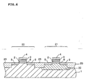
- Fig. 1 is a sectional view showing the first embodiment of the present invention.
- Fig. 2 is a diagram explaining a first manufacturing method relating to the first embodiment of the present invention.
- Fig. 3 is a diagram explaining a second manufacturing method relating to the-first embodiment of the present invention.
- Fig. 4 is a diagram showing an energy band diagram in an MOS structure of the present invention.
- Fig. 5 is a sectional view showing the second embodiment of the present invention.
- Fig. 6 is a sectional view showing the third embodiment of the present invention.
- Fig. 7 is a sectional view showing the fourth embodiment of the present invention.
- Fig. 8 is a diagram showing an example of a related art.
- Fig. 9 is a diagram showing an example of a related art.
- Fig. 1 is a diagram of the case in which the present invention is applied to a p-channel MOSFET.
- the polycrystalline germanium film 3 and the low resistance conductive film 4 are formed through the gate oxide 2 in a region of the p-type silicon substrate 1 where a gate electrode is formed.
- the germanium film 3 may be a single-crystalline germanium or an amorphous germanium film in addition to a polycrystalline germanium layer.
- a germanium film has a characteristic of a p-type semiconductor by doping p-type impurities, e.g. boron (B).
- a channel part 6 is provided and at both ends thereof a source and drain region 5 is provided, thereby forming a MOSFET.
- the use of a germanium film as a gate electrode can suppress the concentration raising of impurities doped in a channel and can prevent the deterioration of carrier mobility in a channel.
- a manufacturing method of the present invention is explained in reference to fig. 2 and fig. 3.
- an NMOS transistor is explained, but a PMOS transistor can also be manufactured in the same way by suitably changing the impurities to be doped to the channel part 6 and the source and drain region 5.
- Fig. 2 shows a first manufacturing method relating to this embodiment.
- borons (B*) are first doped into a p-type silicon substrate 1 having a specific resistance of 14 to 22 ⁇ /cm and the surface orientation (100) to obtain a region with a low concentration of 10 15 to 10 17 cm -3 and to form the channel 6, approximately 70 to 100 angstroms of a gate electrode is formed with thermal oxidation.
- Fig. 2(b) 200 to 400nm of the polycrystalline germanium film 3 is deposited by a CVD (Chemical vapor Deposition) method and borons (B+) are doped into such film by an ion implantation method to obtain a region with a concentration of approximately 10 17 to 10 20 cm -3 .
- CVD Chemical vapor Deposition
- borons (B+) are doped into such film by an ion implantation method to obtain a region with a concentration of approximately 10 17 to 10 20 cm -3 .
- the details on the concentration of borons to be doped into the polycrystalline germanium film 3 at this time is described later.
- a transition metal film e.g. a Ti film is formed by a spattering method, and a part of the polysilicon film 7 becomes a transition metal silicide film 8 (TiSi 2 film) through a high temperature annealing. Further, at this time, all of the polysilicon film 7 can become a refractory silicide. Furthermore, Co, Mo, etc. can be cited as examples of transition metals, in addition to Ti.
- phosphoruses (P+) are doped using this gate electrode pattern as a mask to obtain a region with a concentration of approximately 10 20 cm -3 . Consequently, the source and drain region 5 is obtained by self-alignment.
- the channel part 6 is formed on the p-type silicon substrate 1 having a specific resistance of 14 to 22 ⁇ /cm and the surface orientation (100), and approximately 70 to 100 angstroms of a gate electrode is formed with thermal oxidation.
- the polycrystalline germanium film 3 is deposited on the gate oxide 2 and borons (B+) are doped to become a p-type semiconductor by an ion implantation method.
- a resist not shown in the figure is applied and a gate electrode is patterned by a photo lithography method. Using this gate electrode pattern, the source and drain region 5 is formed by self-alignment.
- the process of up to here is the same as that in the first manufacturing method of Fig. 2.
- silicon dioxide spacers 9 are formed at both ends of the gate electrode, a transition metal film, e.g. a Ti film, Co film or Mo film is formed by a spattering method and a part of the polysilicon film 7 and a surface of the source and drain region 5 becomes the transition metal silicide film 8 through a high temperature annealing.
- the-manufacturing method in the embodiment of the present invention it is possible to bring a work function of a gate electrode close to an intrinsic mid gap energy of silicon, therefore, the concentration raising of impurities doped in a channel can be suppressed, thereby enabling the prevention of deterioration of carrier mobility in the channel.
- Fig. 4 is an energy band diagram of a MOS structure manufactured on the basis of the aforementioned first or second manufacturing method.
- An electron affinity energy ⁇ 1 of a p-type single-crystalline silicon film (channel part) is 4.05eV
- an energy gap E g1 is 1.12eV
- the intrinsic mid gap energy is 4 .61eV
- an electron affinity energy ⁇ 2 is 4.0eV
- an energy gap E g2 is 0.66eV
- an intrinsic mid gap energy E g2 is 4.33eV.
- K B indicates Boltzman's constant
- T indicates absolute temperature
- q indicates quantum of electric charge
- ni indicates an intrinsic carrier concentration of germanium
- Na indicates an impurity concentration doped into a polycrystalline germanium film.
- the required impurity concentration Na can be found as 1.2 X 10 18 cm -3 using the intrinsic carrier concentration of germanium of ni; 2.4 ⁇ 10 13 cm -3 .
- the condition of an ion implantation is that the B + implantation energy is 50keV and the doze amount is approximately 1,0m ⁇ 10 13 cm -2 per a 300nm polycrystalline germanium film thickness.
- the doze amount is no more than 0.01 V according to the formula (1), which shows the high controllability of the work function.
- an electrode of the same material can be used for an n-channel type transistor and a p-channel type transistor, but if any deviation of the work function of a Ti film ⁇ M from the intrinsic mid gap energy of Si causes a difference in a channel dope amount between the n-channel transistor and the p-channel transistor, thereby arising an unbalanced aspect in characteristic.
- a p-type polycrystalline germanium is used for a gate electrode, it is possible to bring such energy close to the intrinsic mid gap energy of Si by using polycrystalline germanium deeply doped to be n+ type. By this, a CMOS well-balanced in the characteristic, in which an electrode of the same material is used, can be obtained.
- the p-type polycrystalline germanium film 3 may also be formed by a CVD method using a mixed gas of GeH 4 and B 2 H 6 . This case brings an advantage that an ion plantation process and an impurity thermal diffusion process required subsequent to such ion implantation process can be omitted.
- the polycrystalline germanium film 3 is formed through the gate oxide 2 in the region of the p-type silicon substrate 1 where a gate electrode is formed.
- a transition metal film 10 is directly formed as a low resistance conductive film by a spattering method.
- Mo, etc. which is chemically stable and has a lower specific resistance among the transition metals, is desirable.
- high temperature annealing is not required. Therefore, this solves a problem that the impurities doped on the p-type polycrystalline germanium film 3 are penetrated into the gate oxide 2.
- this embodiment can be an effective means.
- Reference no. 5 indicates a source and drain region and Reference no. 6 indicates a channel part.
- Fig. 6 indicates a structure in which the PMOS transistor 21 and the NMOS transistor 20 are formed on the p-type silicon substrate 1, and in the region of the PMOS transistor 21 on the p-type silicon substrate 1, an n-well region 22 is formed and is separated from the NMOS transistor 20 through an element separation oxide 23.
- 200 to 400nm of the polycrystalline germanium film 3 is deposited on the gate insulation film 2 by a CVD (Chemical Vapor Deposition) method, and borons (B + ) are deeply doped into such films by an ion implantation method to obtain a region with a concentration of approximately 10 17 to 10 20 cm -3 .
- Reference no. 4 indicates a low resistance conductive film
- Reference no. 5 a source and drain region
- Reference no. 6 a channel part.
- an insulation film 24 is provided on the p-type silicon substrate 1, and the NMOS transistor 20 and the PMOS transistor 21, which have the same structures as those in the second embodiment shown in Fig. 5, are formed on the insulation film 24.
- the work function of the p-type polycrystalline germanium film 3 is also brought close to the intrinsic mid gap energy of silicon. Accordingly, no difference arises as to the concentration of the impurities doped in the channel parts of the NMOS and the PMOS, therefore, a well-balanced CMOS characteristic is obtained.
- MOSFET Silicon on Insulator
- SOI MOSFET is a device structure favorable for speeding up and lowering electric power consumption.
- an embedded oxide silicon dioxide
- an embedding technique techniques of implanting an oxygen ion and of bonding a wafer, on which a thermal oxide is formed, on another wafer, etc. are generally adopted.
- impurities of higher concentration should be doped into such thin film. This may cause the deterioration of carrier mobility. Therefore, compensating this deterioration by controlling the work function in accordance with the present invention, and suppressing the concentration of the impurities to be doped into the channel will be highly effective means for improving carrier mobility.
- a gate electrode can be well-controllably brought close to the intrinsic mid gap energy of silicon, it is possible, whether an NMOS transistor or PMOS transistor, to lower the concentration of impurities in a channel. Therefore, the deterioration of the carrier mobility can be prevented and a MOSFET having a high current driving ability can be provided.
Landscapes
- Metal-Oxide And Bipolar Metal-Oxide Semiconductor Integrated Circuits (AREA)
- Insulated Gate Type Field-Effect Transistor (AREA)
- Electrodes Of Semiconductors (AREA)
Abstract
Description

Claims (13)
- A semiconductor device comprising:a silicon substrate anda metal-oxide-semiconductor field-effect transistor formed on said silicon substrate,wherein a gate electrode of said transistor comprises a germanium film.
- A semiconductor device according to claim 1, wherein said germanium film comprises any one of a single-crystalline germanium film, a polycrystalline germanium film or an amorphous germanium film.
- A semiconductor device according to claim 1 or 2, wherein p-type impurities are doped into said germanium film.
- A semiconductor device according to claim 1, wherein said gate electrode comprises a multi-layer structure that includes a low resistance conductive film.
- A semiconductor device according to claim 4, wherein said low resistance conductive film comprises a transition metal, a transition metal silicide, or a transition metal nitride film, or a combination thereof.
- A semiconductor device according to claim 4, wherein said multi-layer structure is provided with a polysilicon film in between said germanium film and said low resistance conductive film.
- A semiconductor device comprising:an n-channel metal-oxide-semiconductor field-effect transistor anda p-channel metal-oxide-semiconductor field-effect transistor,wherein a gate electrode of each of said transistors comprises any one of a single-crystalline germanium film, a polycrystalline germanium film or an amorphous germanium film in which p-type impurities are doped.
- A manufacturing method of a semiconductor device comprising:a step of forming a gate oxide on a semiconductor substrate;a step of forming a germanium film on said gate oxide;a step of doping p-type impurities into said germanium film and patterning said germanium film to form a gate electrode; anda step of forming a source region and a drain region by using said gate electrode as a mask.
- A manufacturing method of a semiconductor device according to claim 8, wherein the step of forming said gate electrode comprises:a step of forming a polysilicon on said germanium film;a step of forming a transition metal on said polysilicon film; anda step of annealing said polysilicon so that a part or all of said polysilicon becomes a transition metal silicide.
- A manufacturing method of a semiconductor device according to claim 8, wherein the step of forming said gate electrode includes a step of forming a metal transition film or a metal transition nitride film on said germanium film.
- A manufacturing method of a semiconductor device according to claim 8, wherein said p-type impurities are doped by a CVD method.
- A manufacturing method of a semiconductor device according to claim 8, wherein said p-type impurities are doped by an ion implantation method.
- A manufacturing method of a semiconductor device comprising:a step of forming a gate oxide on a substrate of a semiconductor substrate;a step of forming a germanium film on said gate oxide;a step of doping p-type impurities into said germanium film and patterning said germanium film to form a gate electrode;a step of forming a source region and a drain region by using said gate electrode as a mask;a step of forming a spacer on both ends of said gate electrode; anda step of forming a transition metal film on said gate electrode and said source region and a drain region and annealing said transition metal film to form.
Applications Claiming Priority (3)
| Application Number | Priority Date | Filing Date | Title |
|---|---|---|---|
| JP17707899 | 1999-06-23 | ||
| JP17707899 | 1999-06-23 | ||
| PCT/JP2000/003968 WO2000079601A1 (en) | 1999-06-23 | 2000-06-16 | Semiconductor device and method of manufacture thereof |
Publications (2)
| Publication Number | Publication Date |
|---|---|
| EP1111686A1 true EP1111686A1 (en) | 2001-06-27 |
| EP1111686A4 EP1111686A4 (en) | 2005-05-11 |
Family
ID=16024751
Family Applications (1)
| Application Number | Title | Priority Date | Filing Date |
|---|---|---|---|
| EP00937291A Ceased EP1111686A4 (en) | 1999-06-23 | 2000-06-16 | SEMICONDUCTOR DEVICE AND METHOD FOR MANUFACTURING THE SAME |
Country Status (4)
| Country | Link |
|---|---|
| US (1) | US6787805B1 (en) |
| EP (1) | EP1111686A4 (en) |
| KR (1) | KR100695047B1 (en) |
| WO (1) | WO2000079601A1 (en) |
Cited By (3)
| Publication number | Priority date | Publication date | Assignee | Title |
|---|---|---|---|---|
| WO2002009178A3 (en) * | 2000-07-21 | 2002-10-10 | Motorola Inc | Semiconductor device and a process for forming the same |
| DE102004052581A1 (en) * | 2004-10-29 | 2006-05-04 | Advanced Micro Devices, Inc., Sunnyvale | CMOS gate structure having a pre-doped semiconductor gate material with improved uniformity of dopant distribution and methods of fabricating the structure |
| DE102006013721A1 (en) * | 2006-03-24 | 2007-09-27 | Infineon Technologies Ag | Analog silicon-on-insulator semiconductor circuit arrangement, has diode doped region formed in active semiconductor region of specific conductive type up to surface of insulating layer, and measuring diode realized over diode side |
Families Citing this family (7)
| Publication number | Priority date | Publication date | Assignee | Title |
|---|---|---|---|---|
| JP2005531158A (en) * | 2002-06-26 | 2005-10-13 | セムエキップ インコーポレイテッド | Semiconductor device and semiconductor device manufacturing method |
| US6905976B2 (en) * | 2003-05-06 | 2005-06-14 | International Business Machines Corporation | Structure and method of forming a notched gate field effect transistor |
| WO2006012544A2 (en) * | 2004-07-22 | 2006-02-02 | The Board Of Trustees Of The Leland Stanford Junior University | Germanium substrate-type materials and approach therefor |
| JP2006278873A (en) * | 2005-03-30 | 2006-10-12 | Seiko Epson Corp | Semiconductor device and manufacturing method thereof |
| KR100652426B1 (en) * | 2005-08-16 | 2006-12-01 | 삼성전자주식회사 | Capacitor of Semiconductor Device Preventing Dopant Penetration and Its Manufacturing Method |
| WO2021065578A1 (en) * | 2019-10-04 | 2021-04-08 | 国立大学法人東京工業大学 | Light modulation element |
| US20230209795A1 (en) * | 2021-12-23 | 2023-06-29 | Globalfoundries U.S. Inc. | Sram bit cells |
Family Cites Families (20)
| Publication number | Priority date | Publication date | Assignee | Title |
|---|---|---|---|---|
| JPS4822022B1 (en) | 1969-11-21 | 1973-07-03 | ||
| JPS63198373A (en) | 1987-02-13 | 1988-08-17 | Nec Corp | Semiconductor device and its manufacture |
| JP2518334B2 (en) | 1988-01-20 | 1996-07-24 | 日立電線株式会社 | Twist-resistant deformation self-bonding enameled wire |
| JPH01117182A (en) | 1988-06-14 | 1989-05-10 | Kunimune Kogyosho:Kk | Bobbin winder with stopper |
| US5801444A (en) * | 1989-09-29 | 1998-09-01 | International Business Machines Corporation | Multilevel electronic structures containing copper layer and copper-semiconductor layers |
| US5101247A (en) * | 1990-04-27 | 1992-03-31 | North Carolina State University | Germanium silicon dioxide gate MOSFET |
| JP3061406B2 (en) * | 1990-09-28 | 2000-07-10 | 株式会社東芝 | Semiconductor device |
| JP2876866B2 (en) | 1992-02-19 | 1999-03-31 | 日本電気株式会社 | Semiconductor device |
| US5227333A (en) * | 1992-02-27 | 1993-07-13 | International Business Machines Corporation | Local interconnection having a germanium layer |
| AU5669794A (en) | 1992-12-11 | 1994-07-04 | Intel Corporation | A mos transistor having a composite gate electrode and method of fabrication |
| US5572040A (en) * | 1993-07-12 | 1996-11-05 | Peregrine Semiconductor Corporation | High-frequency wireless communication system on a single ultrathin silicon on sapphire chip |
| JPH07202178A (en) | 1993-12-28 | 1995-08-04 | Toshiba Corp | Semiconductor device and manufacturing method thereof |
| JPH07288323A (en) | 1994-04-19 | 1995-10-31 | Sony Corp | Insulated gate type field effect transistor and its manufacturing method |
| US5608249A (en) * | 1995-11-16 | 1997-03-04 | Micron Technology, Inc. | Reduced area storage node junction |
| JPH1027854A (en) * | 1996-07-10 | 1998-01-27 | Sony Corp | Semiconductor device and manufacturing method thereof |
| KR100212693B1 (en) * | 1996-12-14 | 1999-08-02 | 권혁준 | Silicon / Silicon Germanium Morse Field Transistors and Manufacturing Method Thereof |
| JPH113999A (en) | 1997-06-13 | 1999-01-06 | Sony Corp | Method for manufacturing semiconductor device |
| FR2765394B1 (en) * | 1997-06-25 | 1999-09-24 | France Telecom | PROCESS FOR OBTAINING A SILICON-GERMANIUM GRID TRANSISTOR |
| JPH1117182A (en) | 1997-06-26 | 1999-01-22 | Sony Corp | Semiconductor device and manufacturing method thereof |
| JP3039493B2 (en) | 1997-11-28 | 2000-05-08 | 日本電気株式会社 | Substrate cleaning method and cleaning solution |
-
2000
- 2000-06-16 US US09/763,365 patent/US6787805B1/en not_active Expired - Fee Related
- 2000-06-16 WO PCT/JP2000/003968 patent/WO2000079601A1/en not_active Ceased
- 2000-06-16 EP EP00937291A patent/EP1111686A4/en not_active Ceased
- 2000-06-16 KR KR1020017002272A patent/KR100695047B1/en not_active Expired - Fee Related
Cited By (6)
| Publication number | Priority date | Publication date | Assignee | Title |
|---|---|---|---|---|
| WO2002009178A3 (en) * | 2000-07-21 | 2002-10-10 | Motorola Inc | Semiconductor device and a process for forming the same |
| DE102004052581A1 (en) * | 2004-10-29 | 2006-05-04 | Advanced Micro Devices, Inc., Sunnyvale | CMOS gate structure having a pre-doped semiconductor gate material with improved uniformity of dopant distribution and methods of fabricating the structure |
| US7419867B2 (en) | 2004-10-29 | 2008-09-02 | Advanced Micro Devices, Inc. | CMOS gate structure comprising predoped semiconductor gate material with improved uniformity of dopant distribution and method of forming the structure |
| DE102004052581B4 (en) * | 2004-10-29 | 2008-11-20 | Advanced Micro Devices, Inc., Sunnyvale | A method of fabricating a CMOS gate structure having a pre-doped semiconductor material |
| DE102006013721A1 (en) * | 2006-03-24 | 2007-09-27 | Infineon Technologies Ag | Analog silicon-on-insulator semiconductor circuit arrangement, has diode doped region formed in active semiconductor region of specific conductive type up to surface of insulating layer, and measuring diode realized over diode side |
| DE102006013721B4 (en) * | 2006-03-24 | 2011-12-08 | Infineon Technologies Ag | Semiconductor circuit arrangement and associated method for temperature detection |
Also Published As
| Publication number | Publication date |
|---|---|
| WO2000079601A1 (en) | 2000-12-28 |
| EP1111686A4 (en) | 2005-05-11 |
| US6787805B1 (en) | 2004-09-07 |
| KR20010072870A (en) | 2001-07-31 |
| KR100695047B1 (en) | 2007-03-14 |
Similar Documents
| Publication | Publication Date | Title |
|---|---|---|
| JP2978736B2 (en) | Method for manufacturing semiconductor device | |
| US6682965B1 (en) | Method of forming n-and p- channel field effect transistors on the same silicon layer having a strain effect | |
| US6974735B2 (en) | Dual layer Semiconductor Devices | |
| US7508053B2 (en) | Semiconductor MOS transistor device and method for making the same | |
| US7754570B2 (en) | Semiconductor device | |
| US5691225A (en) | Method for fabricating semiconductor device having CMOS structure | |
| WO2011163164A1 (en) | Advanced transistors with threshold voltage set dopant structures | |
| JPH04137528A (en) | Semiconductor device and its manufacture | |
| WO2011163169A1 (en) | Advanced transistors with punch through suppression | |
| EP0676799A2 (en) | Extended drain resurf lateral DMOS devices | |
| US7183182B2 (en) | Method and apparatus for fabricating CMOS field effect transistors | |
| US7645687B2 (en) | Method to fabricate variable work function gates for FUSI devices | |
| US6787805B1 (en) | Semiconductor device and manufacturing method | |
| JPH0951040A (en) | Method for manufacturing semiconductor device | |
| US6417038B1 (en) | Method of fabricating semiconductor device | |
| JP2876866B2 (en) | Semiconductor device | |
| US20070249149A1 (en) | Improved thermal budget using nickel based silicides for enhanced semiconductor device performance | |
| KR101028982B1 (en) | Semiconductor device and manufacturing method thereof | |
| US6905923B1 (en) | Offset spacer process for forming N-type transistors | |
| CN100421255C (en) | Fully depleted SOI multi-threshold voltage applications | |
| US6921709B1 (en) | Front side seal to prevent germanium outgassing | |
| EP1415337A2 (en) | Dual layer cmos devices | |
| JP2011061071A (en) | Semiconductor device and method of manufacturing the same | |
| US20060286759A1 (en) | Metal oxide semiconductor (MOS) device having both an accumulation and a enhancement mode transistor device on a similar substrate and a method of manufacture therefor | |
| JPH10275864A (en) | Method for manufacturing semiconductor device |
Legal Events
| Date | Code | Title | Description |
|---|---|---|---|
| PUAI | Public reference made under article 153(3) epc to a published international application that has entered the european phase |
Free format text: ORIGINAL CODE: 0009012 |
|
| AK | Designated contracting states |
Kind code of ref document: A1 Designated state(s): AT BE CH CY DE DK ES FI FR GB GR IE IT LI LU MC NL PT SE |
|
| AX | Request for extension of the european patent |
Free format text: AL;LT;LV;MK;RO;SI |
|
| 17P | Request for examination filed |
Effective date: 20010530 |
|
| RBV | Designated contracting states (corrected) |
Designated state(s): DE FR GB |
|
| A4 | Supplementary search report drawn up and despatched |
Effective date: 20050331 |
|
| RIC1 | Information provided on ipc code assigned before grant |
Ipc: 7H 01L 21/8238 B Ipc: 7H 01L 29/78 A Ipc: 7H 01L 21/28 B Ipc: 7H 01L 29/49 B |
|
| 17Q | First examination report despatched |
Effective date: 20050630 |
|
| 17Q | First examination report despatched |
Effective date: 20050630 |
|
| STAA | Information on the status of an ep patent application or granted ep patent |
Free format text: STATUS: THE APPLICATION HAS BEEN REFUSED |
|
| 18R | Application refused |
Effective date: 20071016 |