EP1109226A2 - Semiconductor device and its manufacturing method capable of reducing low frequency noise - Google Patents
Semiconductor device and its manufacturing method capable of reducing low frequency noise Download PDFInfo
- Publication number
- EP1109226A2 EP1109226A2 EP00250435A EP00250435A EP1109226A2 EP 1109226 A2 EP1109226 A2 EP 1109226A2 EP 00250435 A EP00250435 A EP 00250435A EP 00250435 A EP00250435 A EP 00250435A EP 1109226 A2 EP1109226 A2 EP 1109226A2
- Authority
- EP
- European Patent Office
- Prior art keywords
- layer
- semiconductor
- semiconductor layer
- diode
- conductivity type
- Prior art date
- Legal status (The legal status is an assumption and is not a legal conclusion. Google has not performed a legal analysis and makes no representation as to the accuracy of the status listed.)
- Withdrawn
Links
Images









Classifications
-
- H—ELECTRICITY
- H10—SEMICONDUCTOR DEVICES; ELECTRIC SOLID-STATE DEVICES NOT OTHERWISE PROVIDED FOR
- H10D—INORGANIC ELECTRIC SEMICONDUCTOR DEVICES
- H10D8/00—Diodes
- H10D8/01—Manufacture or treatment
- H10D8/051—Manufacture or treatment of Schottky diodes
-
- H—ELECTRICITY
- H10—SEMICONDUCTOR DEVICES; ELECTRIC SOLID-STATE DEVICES NOT OTHERWISE PROVIDED FOR
- H10D—INORGANIC ELECTRIC SEMICONDUCTOR DEVICES
- H10D10/00—Bipolar junction transistors [BJT]
- H10D10/80—Heterojunction BJTs
- H10D10/821—Vertical heterojunction BJTs
-
- H—ELECTRICITY
- H10—SEMICONDUCTOR DEVICES; ELECTRIC SOLID-STATE DEVICES NOT OTHERWISE PROVIDED FOR
- H10D—INORGANIC ELECTRIC SEMICONDUCTOR DEVICES
- H10D30/00—Field-effect transistors [FET]
- H10D30/40—FETs having zero-dimensional [0D], one-dimensional [1D] or two-dimensional [2D] charge carrier gas channels
- H10D30/47—FETs having zero-dimensional [0D], one-dimensional [1D] or two-dimensional [2D] charge carrier gas channels having two-dimensional [2D] charge carrier gas channels, e.g. nanoribbon FETs or high electron mobility transistors [HEMT]
- H10D30/471—High electron mobility transistors [HEMT] or high hole mobility transistors [HHMT]
- H10D30/473—High electron mobility transistors [HEMT] or high hole mobility transistors [HHMT] having confinement of carriers by multiple heterojunctions, e.g. quantum well HEMT
- H10D30/4732—High electron mobility transistors [HEMT] or high hole mobility transistors [HHMT] having confinement of carriers by multiple heterojunctions, e.g. quantum well HEMT using Group III-V semiconductor material
-
- H—ELECTRICITY
- H10—SEMICONDUCTOR DEVICES; ELECTRIC SOLID-STATE DEVICES NOT OTHERWISE PROVIDED FOR
- H10D—INORGANIC ELECTRIC SEMICONDUCTOR DEVICES
- H10D8/00—Diodes
- H10D8/60—Schottky-barrier diodes
-
- H—ELECTRICITY
- H10—SEMICONDUCTOR DEVICES; ELECTRIC SOLID-STATE DEVICES NOT OTHERWISE PROVIDED FOR
- H10D—INORGANIC ELECTRIC SEMICONDUCTOR DEVICES
- H10D84/00—Integrated devices formed in or on semiconductor substrates that comprise only semiconducting layers, e.g. on Si wafers or on GaAs-on-Si wafers
- H10D84/01—Manufacture or treatment
-
- H—ELECTRICITY
- H10—SEMICONDUCTOR DEVICES; ELECTRIC SOLID-STATE DEVICES NOT OTHERWISE PROVIDED FOR
- H10D—INORGANIC ELECTRIC SEMICONDUCTOR DEVICES
- H10D84/00—Integrated devices formed in or on semiconductor substrates that comprise only semiconducting layers, e.g. on Si wafers or on GaAs-on-Si wafers
- H10D84/01—Manufacture or treatment
- H10D84/0107—Integrating at least one component covered by H10D12/00 or H10D30/00 with at least one component covered by H10D8/00, H10D10/00 or H10D18/00, e.g. integrating IGFETs with BJTs
-
- H—ELECTRICITY
- H10—SEMICONDUCTOR DEVICES; ELECTRIC SOLID-STATE DEVICES NOT OTHERWISE PROVIDED FOR
- H10D—INORGANIC ELECTRIC SEMICONDUCTOR DEVICES
- H10D84/00—Integrated devices formed in or on semiconductor substrates that comprise only semiconducting layers, e.g. on Si wafers or on GaAs-on-Si wafers
- H10D84/01—Manufacture or treatment
- H10D84/02—Manufacture or treatment characterised by using material-based technologies
- H10D84/05—Manufacture or treatment characterised by using material-based technologies using Group III-V technology
-
- H—ELECTRICITY
- H10—SEMICONDUCTOR DEVICES; ELECTRIC SOLID-STATE DEVICES NOT OTHERWISE PROVIDED FOR
- H10D—INORGANIC ELECTRIC SEMICONDUCTOR DEVICES
- H10D84/00—Integrated devices formed in or on semiconductor substrates that comprise only semiconducting layers, e.g. on Si wafers or on GaAs-on-Si wafers
- H10D84/01—Manufacture or treatment
- H10D84/0112—Integrating together multiple components covered by H10D8/00, H10D10/00 or H10D18/00, e.g. integrating multiple BJTs
Definitions
- the present invention relates to a semiconductor device and its manufacturing method, and more particularly, to a diode such as a Schottky barrier diode (SBD), a tunnel diode and a PIN diode and its manufacturing method.
- a diode such as a Schottky barrier diode (SBD), a tunnel diode and a PIN diode and its manufacturing method.
- a first prior art Schottky barrier diode is of a lateral type which is constructed by a semi-insulating GaAs substrate, an n - -type GaAs contact layer formed on the GaAs substrate, an n + -type GaAs layer formed on the n - -type GaAs contact layer, an anode electrode (Schottky electrode) formed on the n - -type GaAs contact layer, and a cathode electrode (ohmic electrode) formed on the n + -type GaAs layer. This will be explained later in detail.
- a second prior art Schottky barrier diode is of a vertical type which is constructed by a semi-insulating GaAs substrate, an n + -type GaAs contact layer formed on the GaAs substrate, an n - -type GaAs layer formed on the n + -type GaAs layer, an anode electrode (Schottky electrode) formed on the n - -type GaAs layer 203, and a cathode electrode (ohmic electrode) formed on the n + -type GaAs contact layer (see JP-A-8-255838). This also will be explained later in detail.
- the path of the current adjacent to the surface of the n + -type GaAs contact layer is shortened, which would improve the low frequency characteristics.
- Another object is to provide such a semiconductor device incorporating a heterojunction field effect transistor and a heterojunction bipolar transistor and its manufacturing method.
- a first semiconductor layer is formed on a semiconductor substrate.
- a second semiconductor layer is formed on a part of the first semiconductor layer, and a third semiconductor layer is formed on a part of the second semiconductor layer.
- a first electrode is formed on the third semiconductor layer, and a second electrode is formed on the first semiconductor layer in contact with the second semiconductor layer and apart from said the semiconductor layer, thus forming a diode.
- the current path is distant from the surface level of the second semiconductor layer, to improve the low frequency noise characteristics.
- the cathode electrode is buried in the first semiconductor layer so that the current path is further distant from the surface level of the second semiconductor layer, to further improve the low frequency noise characteristics.
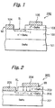
- the Schottky barrier diode SBD is of a lateral type which is constructed by a semi-insulating GaAs substrate 101, an n - -type GaAs contact layer 102 formed on the GaAs substrate 101, an n + -type GaAs layer 103 formed on the n - -type GaAs contact layer 102, an anode electrode 104 formed on the n - -type GaAs contact layer 102, and a cathode electrode 105 formed on the n + -type GaAs layer 103.
- a Schottky barrier SB is generated of at an interface between the anode electrode 104 and the n - -type GaAs contact layer 102.
- the Schottky barrier diode SBD of Fig. 1 since the path of the current I adjacent to the surface of the n - -type GaAs contact layer 102 is relatively long, and, is also very close thereto, the current I is strongly affected by a surface level SL of the n - -type GaAs contact layer 102. As a result, the low frequency noise characteristics of the Schottky barrier diode SBD of Fig. 1 remarkably deteriorate.
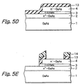
- the Shottky barrie diode SBD is of a vertical type which is constructed by a semi-insulating GaAs substrate 201, an n + -type GaAs contact layer 202 formed on the GaAs substrate 201, an n - -type GaAs layer 203 formed on the n + -type GaAs layer 202, an anode electrode 204 formed on the n - -type GaAs layer 203, and a cathode electrode 205 formed on the n + -type GaAs contact layer 202.
- a Schottky barrier SB is generated at an interface between the anode electrode 204 and the n - -type GaAs layer 203.
- the path of the current I adjacent to the surface of the n + -type GaAs contact layer 202 is shortened, which would improve the low frequency characteristics.
- the Schottky barrier diode SBD of Fig. 2 since the path of the current I adjacent to the surface of the n - -type GaAs contact layer 202 is still close thereto, the current I is still strongly affected by a surface level SL of the n + -type GaAs contact layer 202. As a result, the low frequency noise characteristics of the Schottky barrier diode SBD of Fig. 2 still deteriorate.
- a heterojunction bipolar transistor HBT and a high electron mobility transistor HEMT as well as the Schottky barrier diode SBD of Fig. 2 are formed in one chip.
- the heterojunction bipolar transistor HBT is constructed by an n + -type GaAs sub collector layer 206, an n - -type GaAs collector layer 207, a p + -type GaAs base layer 208 an n-type AlGaAs emitter layer 209, an n + -type GaAs emitter cap layer 210, collector electrodes 211, base electrodes 212 and a collector electrode 213.
- the Schottky barrier diode SBD and the heterojunction bipolar HBT are isolated by a p-type element isolation region 214 formed within the n + -type GaAs layer 202 and the n + -type GaAs layer 206 which are actually the same.
- the high electron mobility transistor HEMT is constructed by a superlattice buffer layer 215, an i-type InGaAs channel layer 216, an n-type silicon planar doped layer 217, an n-type AlGaAs layer donor layer 218, n + -type GaAs source/drain layers 219, a T-shaped gate electrode 220, a source electrode 221, and a drain electrode 222.
- an epitaxial layer for the layers 202, 203, 206, 207, 208, 209 and 210 is grown on the GaAs substrate 201 by a molecular beam epitaxy (MBE) process.
- MBE molecular beam epitaxy
- an area of the epitaxial layer for the high electron mobility transistor HEMT is etched by using a mask which covers an area of the opitaxial layer for the hetro junction bipolar transistor HBT and the Schottky barrier diode SBD.
- another epitaxial layer for the layers 215, 216, 217, 218 and 219 is regrown on the GaAs substrate 201.
- each layer of the epitaxial layers is patterned, and then, each electrode is formed to complete the semiconductor device of Fig. 3.
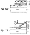
- the Shottky barrie diode SBD is of a vertical type which is constructed by a semi-insulating GaAs substrate 1, an n + -type GaAs contact layer 2 formed on the GaAs substrate 1, an undoped AlGaAs etching stopper layer 3 formed on the n + -type GaAs contact layer 2, an n - -type GaAs layer 4 formed on the i-type AlGaAs etching stopper layer 3, an anode electrode 5 formed on the n - -type GaAs layer 4, and a cathode electrode 6 formed on the n + -type GaAs contact layer 2.
- a Schottky barrier SB is generated at an interface between the anode electrode 5 and the n - -type GaAs layer 4.
- the Schottky barrier diode SBD of Fig. 4 although the path of the current I adjacent to the surface of the n + -type GaAs contact layer 2 is still close thereto, there is no surface level within the n + -type GaAs contact layer 2 due to the presence of the i-type AlGaAs etching stopper layer 3. In this case, a surface level SL may be generated in the i-type AlGaAs etching stopper layer 3; however, the path of the current I is distant from this surface level SL. Therefore, the eurrent I is hardly affected by the surface level SL of the i-type AlGaAs etching stopper layer 3. As a result, the low frequency noise characteristics of the Schottky barrier diode SBD of Fig. 4 can be improved.
- an n + -type GaAs contact layer 2, an i-type AlGaAs etching stopper layer 3 and an n - -type GaAs layer 4 are grown on a semi-insulating GaAs substrate 1 by an MBE process, a metal-organic chemical vapor deposition (MOCVD) process or a vapor-phase epitaxy (VFE) process.
- MOCVD metal-organic chemical vapor deposition
- VFE vapor-phase epitaxy
- a photoresist pattern layer 11 is formed by a photolithography process. Then, the n - -type GaAs layer 4 is etched by a selective dry etching process using BCl 3 gas and the i-type AlGaAs etching stopper layer 3 as an etching stopper. Then, the photoresist pattern layer 11 is removed.
- a photoresist pattern layer 12 is formed by a photolithography process. Then, the i-type AlGaAs etching stopper layer 3 is etched by a wet etching process using hydrogen peroxide water and the n + -type GaAs layer 2 as an etching stopper. Then, the photoresist pattern layer 12 is removed.
- a silicon oxide layer 13 is deposited by a CVD process.
- a photoresist pattern layer 14 is formed by a photolithography process. Then, the silicon oxide layer 13 is etched by a dry etching process using SF 6 gas.
- anode electrode 5 and a cathode electrode 6 are formed by a sputtering process and a lift-off process. Then, the photoresist pattern layer 14 is removed, to obtain the Schottky barrier diode SBD of Fig. 4. Note that the silicon oxide layer 13 is not shown in Fig. 4.
- the AlGaAs etching stopper layer 3 is undoped, the AlGaAs etching stopper layer 3 can be doped, i.e., of an n-type.
- Fig. 6 which illustrates the second embodiment of the diode according to the present invention
- the anode electrode 5 and the cathode electrode 6 of F ⁇ g. 4 are buried in the n - -type GaAs layer 4 and the n + -type GaAs contact layer 2, respectively, of Fig. 4.
- the Schottky barrier diode SBD of Fig. 6 the path of the current I adjacent to the surface of the n + -type GaAs contact layer 2 is distant therefrom, the path of the current I is further distant from the surface level SL. Therefore, the current I is hardly affected by the surface level SL of the i-type AlGaAs etching stopper layer 3. As a result, the low frequency noise characteristics of the Schottky barrier diode SBD of Fig. 6 can be further improved.
- the n + -type GaAs contact layer 2 and the n - -type GaAs layer 4 are etched by a wet etching process using phosphoric acid.
- the etching depth of the n + -type GaAs contact layer 2 and the n - -type GaAs layer 4 is about 100 ⁇ .
- the anode electrode 5 and the cathode electrode 6 are formed by a sputtering process and a lift-off process.
- the photoresist pattern layer 14 is removed, to obtain the Schottky barrier diode SBD of Fig. 6. Note that the silicon oxide layer 13 is not shown in Fig. 6.
- the AlGaAs etching stopper layer 3 is undoped, the AlGaAs etching stopper layer 3 can be doped, i.e., of an n-type.
- Fig. 8 which illustrates the third embodiment of the diode according to the present invention, the i-type GaAs etching stopper layer 3 of Fig. 6 is omitted.
- the path of the current I adjacent to the surface of the n + -type GaAs contact layer 2 is distant therefrom, the path of the current I is distant from the surface level SL within the n + -type GaAs contact layer 2. Therefore, the current I is hardly affected by the surface level SL of the n + -type GaAs layer 2. As a result, the low frequency noise characteristics of the Schottky barrier diode SBD of Fig. 8 can be improved.
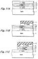
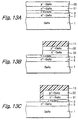
- an n + -type GaAs contact layer 2 and an n - -type GaAs layer 4 are grown on a semi-insulating GaAs substrate 1 by an MBE process, an MOCVD process or a VPE process.
- a photoresist pattern layer 11 is formed by a photolithography process. Then, the n - -type GaAs layer 4 is etched by a selective dry etching process using BCl 3 gas. Then, the photoresist pattern layer 11 is removed.
- a silicon oxide layer 13 is deposited by a CVD process.
- a photoresist pattern layer 14 is formed by a photolithography process. Then, the silicon oxide layer 13 is etched by a dry etching process using SF 6 gas.
- the n + -type GaAs contact layer 2 and the n - -type GaAs layer 4 are etched by a wet etching process using phosphoric acid.
- the etching depth of the n + -type GaAs contact layer 2 and the n - -type GaAs layer 4 is about 100 ⁇ .
- the anode electrode 5 and the cathode electrode 6 are formed by a sputtering process and a lift-off process.
- the photoresist pattern layer 14 is removed, to obtain the Schottky barrier diode SBD of Fig. 8. Note that the silicon oxide layer 13 is not shown in Fig. 8.
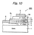
- Fig. 10 which illustrates the fourth embodiment of the diode according to the present invention that is, in this case, a Schottky barrier diode SBD, an i-type GaAs layer 21 and an i-type AlGaAs etching stopper layer 22 are added to the Schottky barrier diode SBD of Fig. 4.
- a surface level SL may be generated in the i-type AlGaAs etching stopper layer 22; however, the path of the current I is far away from this surface level SL. Therefore, the current I is hardly affected by the surface level SL of the i-type AlGaAs etching stopper layer 22. As a result, the low frequency noise characteristics of the Schottky barrier diode SBD of Fig. 10 can be further improved.
- the n + -type GaAs contact layer 2, the i-type AlGaAs etching stopper layer 3, an i-type GaAs layer 21, an i-type AlGaAs etching stopper layer 22 andthe n - -type GaAs layer 4 are grown on a semi-insulating substrate 1 by an MBE process, an MOCVD process or a VPE process.
- the i-type AlGaAs etching stopper layers 3 and 22 are about 50 ⁇ thick.
- the photoresist pattern layer 11 is formed by a photolithography process. Then, the n - -type GaAs layer 4 is etched by a 1 selective dry etching process using BCl 3 gas and the i-type AlGaAs etching stopper layer 22 as an etching stopper. Then, the photoresist pattern layer 11 is removed.
- the photoresist pattern layer 12 is formed by a photolithography process.
- the i-type AlGaAs etching stopper layer 22 is etched by a wet etching process using hydrogen peroxide water and the i-type GaAs layer 21 as an etching stopper.
- the i-type GaAs layer 21 is etched by a 1 selective dry etching process using BCl 3 gas and the i-type AlGaAs etching stopper layer 3 as an etching stopper.
- the i-type AlGaAs etching stopper layer 3 is etched by a wet etching process using hydrogen peroxide water and the n + -type GaAs layer 3 as an etching stopper. Then, the photoresist pattern layer 12 is removed.
- the silicon oxide layer 13 is deposited by a CVD process.
- the photoresist pattern layer 14 is formed by a photolithography process. Then, the silicon oxide layer 13 is etched by a dry etching process using SF 6 gas.
- the anode electrode 5 and the cathode electrode 6 are formed by a sputtering process and a lift-off process. Then, the photoresist pattern layer 14 is removed, to obtain the Schottky barrier diode SBD of Fig. 10. Note that the silicon oxide layer 13 is not shown in Fig. 10.
- the AlGaAs etching stopper layers 3 and 22 are undoped, the AlGaAs etching stopper layers 3 and 22 can be doped, i.e., of an n-type.
- the cathode electrode 6 can be buried in the n + -type GaAs contact layer 2 in the same way as in the third embodiment, so as to further improve the low frequency noise characteristics.
- the tunnel diode TD is of a vertical type which is constructed by a semi-insulating GaAs substrate 1, the n + -type GaAs contact layer 2 formed on the GaAs substrate 1, the undoped AlGaAs etching stopper layer 3 formed on the n + -type GaAs contact layer 2, an n + -type GaAs layer 31 formed on the i-type AlGaAs etching stopper layer 3, a p + -type GaAs layer 32 formed on the n + -type GaAs layer 31, the anode electrode 5 formed on the p + -type GaAs layer 32, and the cathode electrode 6 formed on the n + -type GaAs contact layer 2.
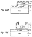
- the n + -type GaAs contact layer 2, the i-type AlGaAs etching stopper layer 3, the n + -type GaAs layer 31, the p + -type GaAs layer 32 and the n - -type GaAs layer 4 are grown on the semi-insulating substrate 1 by an MBE process, an MOCVD process or a VPE process.
- the i-type AlGaAs etching stopper layer 3 is about 50 ⁇ thick.
- the photoresist pattern layer 11 is formed by a photolithography process. Then, the p + -type GaAs layer 32 and the n + -type GaAs layer 31 are etched by a 1 selective dry etching process using BCl 3 gas and the i-type AlGaAs etching stopper layer 3 as an etching stopper. Then, the photoresist pattern layer 11 is removed.
- the photoresist pattern layer 12 is formed by a photolithography process. Then, the i-type AlGaAs etching stopper layer 3 is etched by a wet etching process using hydrogen peroxide water and the n + -type GaAs layer 2 as an etching stopper. Then, the photoresist pattern layer 12 is removed.
- the silicon oxide layer 13 is deposited by a CVD process.
- the photoresist pattern layer 14 is formed by a photolithography process. Then, the silicon oxide layer 13 is etched by a dry etching process using SF 6 gas.
- the anode electrode 5 and the cathode electrode 6 are formed by a sputtering process and a lift-off process. Then, the photoresist pattern layer 14 is removed, to obtain the tunnel diode TD of Fig. 12. Note that the silicon oxide layer 13 is not shown in Fig. 12.
- the AlGaAs etching stopper layer 3 is undoped, the AlGaAs etching stopper layer 3 can be doped, i.e., of an n-type.
- the cathode electrode 6 can be buried in the n + -type GaAs contact layer 2 in the same way as in the third embodiment, so as to further improve the low frequency noise characteristics.
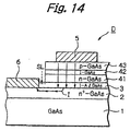
- the PIN diode D is of a vertical type which is constructed by the semi-insulating GaAs substrate 1, the n + -type GaAs contact layer 2 formed on the GaAs substrate 1, the undoped AlGaAs etching stopper layer 3 formed on the n + -type GaAs contact layer 2, an n-type GaAs layer 41 formed on the i-type AlGaAs etching stopper layer 3, an i-type GaAs layer 42 formed on the n-type GaAs layer 41 a p-type GaAs layer 43 formed on the i-type GaAs layer 42, the anode electrode 5 formed on the p-type GaAs layer 43, and the cathode electrode 6 formed on the n + -type GaAs contact layer 2.
- the n + -type GaAs contact layer 2, the i-type AlGaAs etching stopper layer 3, the n-type GaAs layer 41,the i-type GaAs layer 42 a p-type GaAs layer 43 and the n - -type GaAs layer 4 are grown on the semi-insulating substrate 1 by an MBE process, an MOCVD process or a VPE process.
- the i-type AlGaAs etching stopper layer 3 is about 50 ⁇ thick.
- the photoresist pattern layer 11 is formed by a photolithography process. Then, the p-type GaAs layer 43, the i-type GaAs layer 42 and the n-type GaAs layer 41 are etched by a 1 selective dry etching process using BCl 3 gas and the i-type AlGaAs etching stopper layer 3 as an etching stopper. Then, the photoresist pattern layer 11 is removed.
- the photoresist pattern layer 12 is formed by a photolithography process. Then, the i-type AlGaAs etching stopper layer 3 is etched by a wet etching process using hydrogen peroxide water and the n + -type GaAs layer 2 as an etching stopper. Then, the photoresist pattern layer 12 is removed.
- the silicon oxide layer 13 is deposited by a CVD process.
- the photoresist pattern layer 14 is formed by a photolithography process. Then, the silicon oxide layer 13 is etched by a dry etching process using SF 6 gas.
- the anode electrode 5 and the cathode electrode 6 are formed by a sputtering process and a lift-off process. Then, the photoresist pattern layer 14 isremoved, to obtain the PIN diode D of Fig. 14. Note that the silicon oxide layer 13 is not shown in Fig. 14.
- the AlGaAs etching stopper layer 3 is undoped, the AlGaAs etching stopper layer 3 can be doped, i.e., of an n-type.
- the cathode electrode 6 can be buried in the n + -type GaAs contact layer 2 in the same way as in the third embodiment, so as to further improve the low frequency noise characteristics.
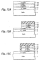
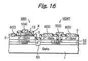
- Fig. 16 is a cross-sectional view illustrating a semiconductor device in which the Schottky diode SBD of Fig. 6 is combined with a high electron mobility transistor HEMT.
- an i-type InGaAs channel layer 51 and an n-type AlGaAs electron supply layer 52 are formed on the GaAs substrate 1 for the high electron mobility transistor HEMT.
- the i-type InGaAs channel layer 51 and the n-type AlGaAs electron supply layer 52 are meaningless for the Schottky barrier diode SBD.
- the Schottky barrier diode SBD and the high electron mobility transistor HEMT are isolated from each other by a p + -type isolation region 53.
- a gate electrode 5(G) is made of the same material as the anode electrode 5(A)
- a source electrode 6(S) and a drain electrode 6(D) are made of the same material as the cathode electrode 6(C).
- the i-type InGaAs channel layer 51, the n-type AlGaAs electron supply layer 52, the n + -type GaAs contact layer 2, the i-type AlGaAs etching stopper layer 3 and an n - -type GaAs layer 4 are grown on the semi-insulating GaAs substrate 1 by an MBE process, a MOCVD process or a VPE process.
- the i-type AlGaAs etching stopper layer 3 is about 50 ⁇ thick.
- the photoresist pattern layer 11 is formed by a photolithography process. Then, the n - -type GaAs layer 4 is etched by a selective dry etching process using BCl 3 gas and the i-type AlGaAs etching stopper layer 3 as an etching stopper. Then, the photoresist pattern layer 11 is removed.
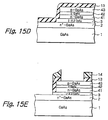
- a photoresist pattern layer 54 is formed by a photolithography process. Then, boron ions are implanted into the GaAs substrate 1 as well as the layers 51, 52, 2 and 3. As a result, a p + -type isolation region 53 is formed. Then, the photoresist pattern 54 is removed.
- the photoresist pattern layer 12 is formed by a photolithography process. Then, the i-type AlGaAs etching stopper layer 3 is etched by a wet etching process using hydrogen peroxide water and the n + -type GaAs layer 2 as an etching stopper. Then, the photoresist pattern layer 12 is removed.
- a photoresist pattern layer 55 is formed by a photolithography process. Then, the n + -type GaAs layer 2 is etched by a 1 selective dry etching process using BCl 3 gas and the n-type AlGaAs, etching stopper layer 52 as an etching stopper. Then, the photoresist pattern layer 55 is removed.
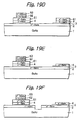
- the silicon oxide layer 13 is deposited by a CVD process.
- the silicon oxide layer 13 is perforated by a photolithography and dry etching process using SF 6 gas to form openings for the anode electrode 5(A) and the gate electrode 5(G). Then, the anode electrode 5(A) and the gate electrode 5(G) are buried in the openings by a sputtering and lift-off process.
- the silicon oxide layer 13 is perforated by a photolithography and dry etching process using SF 6 gas to form openings for the cathode electrode 6(C), the source electrode 5(G), 6(S) and the drain electrode 6(D).
- the n + -type GaAs contact layer 2 is etched by a wet etching process using phosphoric acid. In this case, the etching depth of the n + -type GaAs contact layer 2 is about 100 ⁇ .
- the cathode electrode 6(C), the source electrode 6(C) and the drain electrode 6(D) are buried in the openings by a sputtering and lift-off process, to obtain the semiconductor device of Fig. 16.
- the AlGaAs etching stopper layer 3 is undoped, the AlGaAs etching stopper layer 3 can be doped, i.e., of an n-type. Also, the anode electrode 5(A) can be buried in the n - -type GaAs layer 4, and the gate electrode 5(G) can be buried in the n-type AlGaAs layer 52.
- Fig. 18 is a cross-sectional view illustrating a semiconductor device in which the Schottky diode SBD of Fig. 6 is combined with a heterojunction bipolar transistor HBT.
- the InGaAs etching stopper layer 3 is of an n-type. Also, the n + -type GaAs contact layer 2 of the heterojunction bipolar transistor HBT serves as a collector contact layer, and the n-type GaAs layer 3 and the n-type GaAs layer 4 serve as a collector layer.
- the heterojunction bipolar transistor HBT is constructed by a p + -type GaAs base layer 61, an n-type AlGaAs emitter layer 62 and a n + -type InGaAs emitter cap layer 63.
- reference numeral 6(C') designates a collector electrode
- 65 designates a base electrode
- 66 designates an emitter electrode.
- the collector electrode 6(C') are made of the same material as the cathode electrode 6(C).
- the n + -type GaAs contact layer 2, then-type AlGaAs etching stopper layer 3,the n - -type GaAs layer 4, the p + -type GaAs base layer 61, the n-type AlGaAs emitter layer 62, and the n + -type InGaAs emitter cap layer 63 are grown on the semi-insulating GaAs substrate 1 by an MBE process, a MOCVD process or a CVE process.
- the n-type AlGaAs etching stopper layer 3 is about 50 ⁇ thick.
- a photoresist pattern layer (not shown) is formed by a photolithography process to cover an emitter area. Then, the n + -type InGaAs emitter cap layer 63 and the n-AlGaAs emitter layer 62 are etched by a wet or dry etching process using the photoresist pattern as a mask.
- a photoresist pattern layer (not shown) is formed by a photolithography process to cover a base area and an anode area. Then, the p + -type GaAs layer 61 and the n - -GaAs layer 4 are etched by a selective dry etching process using BCl 3 gas and the photoresist pattern as a mask.
- a photoresist pattern layer (not shown) is formed by a photolithography process to cover an area adjacent to the anode area. Then, the n-type InGaAs etching stopper layer 3 is etched by a wet etching process using hydrogen peroxide water.
- a photoresist pattern layer (not shown) is formed by a photolithography process to cover an area other than the anode area. Then, the p + -type GaAs layer 61 of the anode area is etched by a selective dry etching process using BCl 3 gas and the photoresist pattern layer as a mask.
- a photoresist patter layer (not shown) is formed by a photolithography process to cover an area where the Schottky barrier diode SBD and the heterojunction bipolar transistor HBT will be formed. Then, the n + -type GaAs contact layer 2 and the GaAs substrate 1 are etched by using the photoresist pattern layer as a mask.
- the silicon oxide layer 13 is deposited by a CVD process.
- the silicon oxide layer 13 is perforated by a photolithography and dry etching process using SF 6 gas to form openings for the anode electrode 5(A), the base electrode 65 and the emitter electrode 66. Then, the anode electrode 5(A), the base electrode 65 and the emitter electrode 66 are buried in the openings by a sputtering and lift-off process.
- the silicon oxide layer 13 is perforated by a photolithography and dry etching process using SF 6 gas to form openings for the cathode electrode 6(C) and the collector electrode 6(C').
- the n + -type GaAs contact layer 2 is etched by a wet etching process using phosphoric acid.
- the etching depth of the n + -type GaAs contact layer 2 is about 100 ⁇ .
- the cathode electrode 6(C) and the collector electrode 6(C') are buried in the openings by a sputtering and lift-off process, to obtain the semiconductor device of Fig. 18.
- the anode electrode 5(A) can be buried in the n - -type GaAs layer 4
- the base electrode 65 can be buried in the p + -type GaAs base layer 61
- the emitter electrode 66 can be buried in the n + -type InGaAs emitter cap layer 63.
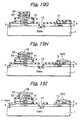
- Fig. 20 is a cross-sectional view illustrating a semiconductor device in which the Schottky diode SBD of Fig. 6 is combined with a high electron mobility transistor HEMT and a heterojunction bipolar transistor HBT.
- the semiconductor device of Fig. 16 and the semiconductor device of Fig. 18 are combined altogether.
- the i-type InGaAs channel layer 51 and the n-type AlGaAs electron supply layer 52 are also formed in the heterojunction bipolar transistor HBT, however, the i-type InGaAs channel layer 51 and the n-type AlGaAs electron supply layer 52 are meaningless for the heterojunction bipolar transistor HBT.
- one eptaxial layer is grown on the GaAs substrate 1. That is, as illustrated in Fig. 21, the i-type InGaAs channel layer 51, the n-type AlGaAs electron supply layer 52, an n + -type GaAs contact layer 2, the n-type AlGaAs etching stopper layer 3, the n - -type GaAs layer 4, the p + -type GaAs base layer 61, the n-type AlGaAs emitter layer 62, and the n + -type InGaAs emitter cap layer 63 are grown on the semi-insulating GaAs substrate 1 by an MBE process, a MOCVD process or a VPE process. In this case, the n-type AlGaAs etching stopper layer 3 is about 50 ⁇ thick.
- the Schottky barrier diode of Fig. 6 is combined with a high electron mobility transistor HEMT and/or a heterojunction bipolar transistor HBT
- the Schottky barrier diode SBD of Figs. 4 and 7 the tunnel diode TD of Fig. 8 and the PIN diode of Fig. 10 can be combined with a high electron mobility transistor HEMT and/or a heterojunction bipolar transistor HBT.
- the path of a current is distant from the surface level which would generate low frequency noise, the low frequency characteristics can be improved.
Landscapes
- Electrodes Of Semiconductors (AREA)
- Junction Field-Effect Transistors (AREA)
- Element Separation (AREA)
- Semiconductor Integrated Circuits (AREA)
- Bipolar Integrated Circuits (AREA)
- Bipolar Transistors (AREA)
Abstract
Description
by a surface level of the n--type GaAs contact layer. As a result, the low frequency noise characteristics such as 1/f noise of the Schottky barrier diode remarkably deteriorates.
Claims (42)
- A semiconductor device comprising:a semiconductor substrate (1);a first semiconductor layer (2) formed on said semiconductor substrate;a second semiconductor layer (3) formed on a part of said first semiconductor layer;a third semiconductor layer (4) formed on a part of said second semiconductor layer;a first electrode (5) formed on said third semiconductor layer; anda second electrode (6) formed on said first semiconductor layer in contact with said second semiconductor layer and apart from said third semiconductor layer,thus forming a diode.
- The semiconductor device as set forth in claim 1, wherein said first and third semiconductor layers (2, 4) are of one conductivity type, and said second semiconductor layer (3) is undoped, so that said diode is a Schottky barrier diode.
- The semiconductor device as set forth in claim 1, wherein said first, second and third semiconductor layers (2, 3, 4) are of one conductivity type, so that said diode is a Schottky barrier diode.
- The semiconductor device as set forth in claim 1, wherein said first and third semiconductor layers (2, 4) have a different material from that of said second semiconductor layer (2).
- The semiconductor device as set forth in claim 1, wherein said second electrode is buried in said first semiconductor layer,
- The semiconductor device as set forth in claim 1, further comprising:a fourth semiconductor layer (21) formed on said second semiconductor layer; anda fifth semiconductor layer (22) formed on said fourth semiconductor layer,said second and fifth semiconductor layers being made of a material different from that of said first, third and fourth semiconductor layers.
- The semiconductor device as set forth in claim 1, further comprising a fourth semiconductor layer (32) formed on said third semiconductor layer,
said first and third semiconductor layers (2, 31) being of a first conductivity type, said fourth semiconductor layer (32) being a second conductivity type opposite to said first conductivity type, so that said diode is a tunnel diode. - The semiconductor device as set forth in claim 6, wherein said second semiconductor layer is undoped.
- The semiconductor device as set forth in claim 6, wherein said second semiconductor layer is of said first conductivity type.
- The semiconductor device as set forth in claim 1, further comprising:a fourth semiconductor layer (42) of an i-type conductivity type formed on said third semiconductor layer; anda fifth semiconductor layer (43) formed on said fourth semiconductor layer,said first and third semiconductor layers being of a first conductivity type, said fifth semiconductor layer being of a second conductivity type opposite to said first conductivity type, so that said diode is a PIN diode.
- The semiconductor device as set forth in claim 10, wherein said second semiconductor layer is undoped.
- The semiconductor device as set forth in claim 10, wherein said second semiconductor layer is of said first conductivity type.
- The semiconductor device as set forth in claim 1, further comprising:an i-type channel layer (51) between said semiconductor substrate and said first semiconductor layer; anda charge supply layer (52) formed between said i-type channel layer and said first semiconduct layer,said i-type channel layer, said charge supply layer and said first semiconductor layer forming a heterojunction field effect transistor (HEMT) separated from said diode.
- The semiconductor device as set forth in claim 13, wherein said diode and said field effect transistor are separated by an isolation region (53) therebetween in said i-type channel layer and said charge supply layer.
- The semiconductor device as set forth in claim 1, further comprising;a semiconductor base layer (61) having a conductivity type opposite to that of said third semiconductor layer formed on said third semiconductor layer;a semiconductor emitter layer (62) having the same conductivity type as that of said third semiconductor layer formed on said semiconductor base layer; anda semiconductor emitter cap layer (63) having the same conductivity type as that of said third semiconductor layer formed on said semiconductor emitter layer;said first, second and third semiconductor layers, said semiconductor base layer, said semiconductor emitter layer and said semiconductor emitter cap layer forming a heterojunction bipolar transistor (HBT) separated from said diode.
- The semiconductor device as set forth in claim 15, wherein said diode and said bipolar transistor are separated by a groove formed in said first semiconductor layer and said semiconductor substrate.
- A semiconductor device comprising:a semiconductor substrate (1);a first semiconductor layer (2) formed on said semiconductor substrate;a second semiconductor layer (4) formed on a part of said first semiconductor layer;a first electrode (5) formed on said second semiconductor layer; anda second electrode (6) buried in said first semiconductor layer and apart from said second semiconductor layer,thus forming a diode.
- The semiconductor device as set forth in claim 17, wherein said first and second semiconductor layers (2, 4) are of one conductivity type, so that said diode is a Schottky barrier diode.
- The semiconductor device as set forth in claim 17, further comprising:a third semiconductor layer (21) formed on said first semiconductor layer; anda fourth semiconductor layer (22) formed on said third semiconductor layer,said second and fourth semiconductor layers being made of a material different from that of said first, second and third semiconductor layers.
- The semiconductor device as set forth in claim 17, further comprising a third semiconductor layer (32) formed on said second semiconductor layer,
said first and second semiconductor layers (2, 31) being of a first conductivity type, said third semiconductor layer (32) being a second conductivity type opposite to said first conductivity type, so that said diode is a tunnel diode. - The semiconductor device as set forth in claim 17, further comprising:a third semiconductor layer (42) of an i-type conductivity type second on said second semiconductor layer; anda fourth semiconductor layer (43) formed on said third semiconductor layer,said first and second semiconductor layers being of a first conductivity type, said fourth semiconductor layer being of a second conductivity type opposite to said first conductivity type, so that said diode is a PIN diode.
- The semiconductor device as set forth in claim 17, further comprising:an i-type channel layer (51) between said semiconductor substrate and said first semiconductor layer: anda charge supply layer (52) formed between said i-type channel layer and said first semiconductor layer,said i-type channel layer, said charge supply layer and said first semiconductor layer forming a heterojunction field effect transistor (HEMT) separated from said diode.
- The semiconductor device as set forth in claim 22, wherein said diode and said field effect transistor are separated by an isolation region (53) therebetween in said i-type channel layer and said charge supply layer.
- The semiconductor device as set forth in claim 17, further comprising:a semiconductor base layer (61) having a conductivity type opposite to that of said third semiconductor layer formed on said second semiconductor layer;a semiconductor emitter layer (62) having the same conductivity type as that of said second semiconductor layer formed on said semiconductor base layer; anda semiconductor emitter cap layer (63) having the same conductivity type as that of said second semiconductor layer formed on said semiconductor emitter layer,said first and second semiconductor layers, said semiconductor base layer, said semiconductor emitter layer and said semiconductor emitter cap layer forming a heterojunction bipolar transistor (HBT) separated from said diode.
- The semiconductor device as set forth in claim 24, wherein said diode and said bipolar transistor are separated by a groove formed in said first semiconductor layer and said semiconductor substrate.
- A method for manufacturing a semiconductor device, comprising the steps of:forming first, second and third semiconductor layers (2, 3, 4) on a semiconductor substrate (1) by an epitaxial growing process;patterning said third semiconductor layer by an etching process using said second semiconductor layer as an etching stopper;patterning said second semiconductor layer by an etching process using said first semiconductor layer as an etching stopper, so that said third semiconductor layer is formed on a part of said second semiconductor layer;forming a first electrode (5) on said third semiconductor layer; andforming a second electrode (6) on said first semiconductor layer adjacent to said second semiconductor layer and apart from said third semiconductor layer,thus completing a diode.
- The method as set forth in claim 26, further comprising a step of partly etching said first semiconductor layer after said second semiconductor layer is patterned and before said second electrode is formed, so that said second electrode is buried in said first semiconductor layer.
- The method as set forth in claim 26, wherein said epitaxial growing step further forms a fourth semiconductor layer (21) and a fifth semiconductor layer (22) between said second and fourth semiconductor layers,
said second and fifth semiconductor layers being made of a material different from that of said first, third and fourth semiconductor layers. - The method as set forth in claim 26, wherein said epitaxial growing step further forms a fourth semiconductor layer (32) on said third semiconductor layer,
said first and third semiconductor layers (2, 31) being of a first conductivity type, said fourth semiconductor layer (32) being a second conductivity type opposite to said first conductivity type, so that said diode is a tunnel diode. - The method as set forth in claim 26, wherein said epitaxial growing step further forms a fourth semiconductor layer (42) of an i-type conductivity type and a fifth semiconductor layer (43) on said fourth semiconductor layer,
said first and third semiconductor layers being of a first conductivity type, said fifth semiconductor layer being of a second conductivity type opposite to said first conductivity type, so that said diode is a PIN diode. - The method as set forth in claim 26, wherein said epitaxial growing step further forms an i-type channel layer (51) and a charge supply layer (52) between said semiconductor substrate and said first semiconduct layer,
said i-type channel layer, said charge supply layer and said first semiconductor layer forming a heterojunction field effect transistor (HEMT) separated from said diode. - The method as set forth in claim 31, further comprising a step of forming an isolation region (53) in said i-type channel layer and said charge supply layer, so that said diode and said field effect transistor are separated by said isolation region.
- The method as set forth in claim 26, wherein said epitaxial growing step further forms a semiconductor base layer (61) having a conductivity type opposite to that of said third semiconductor layer;a semiconductor emitter layer (62) having the same conductivity type as that of said third semiconductor layer, and a semiconductor emitter cap layer (63) having the same conductivity type as that of said third semiconductor layer on said third semiconductor layer;said first, second and third semiconductor layers, said semiconductor base layer, said semiconductor emitter layer and said semiconductor emitter cap layer forming a hetero junction bipolar transistor (HBT) separated from said diode.
- The method as set forth in claim 33 , further comprising a step of forming a groove in said first semiconductor layer and said semiconductor substrate, so that said diode and said bipolar transistor are separated by said groove,
- A method for manufacturing a semiconductor device, comprising the steps of:forming first and second semiconductor layers (2, 4) on a semiconductor substrate (1) by an epitaxial growing process substrate;patterning said second semiconductor layer so that said second semiconductor layer is formed on a part of said first semiconductor layer;partly etching said first semiconductor layer after said second semiconductor layer is patterned;forming a first electrode (5) on said second semiconductor layer; andburying a second electrode (6) in said first semiconductor layer and apart from said second semiconductor layer,thus forming a diode.
- The method as set forth in claim 35, wherein said epitaxial growing step further forms a third semiconductor layer (21) and a fourth semiconductor layer (22) between.said first and third semiconductor layers,
said third semiconductor layer being made of a material different from that of said first and second semiconductor layers. - The method as set forth in claim 35, wherein said epitaxial process further forms a third semiconductor layer (32) on said second semiconductor layer,
said first and second semiconductor layers (2, 31) being of a first conductivity type, said third semiconductor layer (32) being a second conductivity type opposite to said first conductivity type, so that said diode is a tunnel diode. - The method as set forth in claim 35, wherein said epitaxial growing step further forms a third semiconductor layer (42) of an i-type conductivity type and a fourth semiconductor layer (43) on said second semiconductor layer,
said first and second semiconductor layers being of a first conductivity type, said fourth semiconductor layer being of a second conductivity type opposite to said first conductivity type, so that said diode is a PIN diode. - The method as set forth in claim 35, wherein said epitaxial growing step further forms an i-type channel layer (51) and a charge supply layer (52) between said first semiconductor substrate and said first semiconduct layer,
said i-type channel layer, said charge supply layer and said first semiconductor layer forming a field effect transistor (HEMT) having hetero junctions separated from said diode. - The method as set forth in claim- 39, further comprising a step of forming an isolation region (53) in said i-type channel layer and said charge supply layer, so that said diode and said field effect transistor are separated by said isolation region (53).
- The method as set forth in claim 35, wherein said epitaxial growing step further forms a semiconductor base layer (61) having a conductivity type opposite to that of said third semiconductor layer, a semiconductor emitter layer (62) having the same conductivity type as that of said second semiconductor layer, and a semiconductor emitter cap layer (63) having the same conductivity type as that of said second semiconductor layer on said second semiconductor layer,
said first and second semiconductor layers, said semiconductor base layer, said semiconductor emitter layer and said semiconductor emitter cap layer forming a heterojunction bipolar transistor (HBT) separated from said diode . - The method as set forth in claim 41, further comprising a step of forming a groove formed in said first semiconductor layer and said semiconductor substrate, so that said diode and said bipolar transistor are separated by said groove.
Applications Claiming Priority (2)
| Application Number | Priority Date | Filing Date | Title |
|---|---|---|---|
| JP35511399 | 1999-12-14 | ||
| JP35511399A JP2001177060A (en) | 1999-12-14 | 1999-12-14 | Monolithic integrated circuit device and method of manufacturing the same |
Publications (2)
| Publication Number | Publication Date |
|---|---|
| EP1109226A2 true EP1109226A2 (en) | 2001-06-20 |
| EP1109226A3 EP1109226A3 (en) | 2004-01-14 |
Family
ID=18442020
Family Applications (1)
| Application Number | Title | Priority Date | Filing Date |
|---|---|---|---|
| EP00250435A Withdrawn EP1109226A3 (en) | 1999-12-14 | 2000-12-14 | Semiconductor device and its manufacturing method capable of reducing low frequency noise |
Country Status (3)
| Country | Link |
|---|---|
| US (2) | US6525346B2 (en) |
| EP (1) | EP1109226A3 (en) |
| JP (1) | JP2001177060A (en) |
Cited By (2)
| Publication number | Priority date | Publication date | Assignee | Title |
|---|---|---|---|---|
| US20160005848A1 (en) * | 2010-06-24 | 2016-01-07 | Fujitsu Limited | Semiconductor device |
| CN116598310A (en) * | 2023-07-17 | 2023-08-15 | 河源市众拓光电科技有限公司 | GaN-based wide-input-power-range rectifying chip, manufacturing method thereof and rectifier |
Families Citing this family (30)
| Publication number | Priority date | Publication date | Assignee | Title |
|---|---|---|---|---|
| DE10102201C2 (en) * | 2001-01-18 | 2003-05-08 | Epcos Ag | Electrical switching module, switching module arrangement and use of the switching module and the switching module arrangement |
| US6946717B2 (en) * | 2001-01-30 | 2005-09-20 | M/A-Com, Inc. | High voltage semiconductor device |
| JP2005026242A (en) * | 2001-07-19 | 2005-01-27 | Advantest Corp | Semiconductor device and method for manufacturing semiconductor device |
| US20050059371A1 (en) * | 2001-09-28 | 2005-03-17 | Christian Block | Circuit arrangement, switching module comprising said circuit arrangement and use of switching module |
| US6852615B2 (en) * | 2002-06-10 | 2005-02-08 | Hrl Laboratories, Llc | Ohmic contacts for high electron mobility transistors and a method of making the same |
| DE10246098A1 (en) * | 2002-10-02 | 2004-04-22 | Epcos Ag | circuitry |
| JP4954463B2 (en) * | 2004-10-22 | 2012-06-13 | 三菱電機株式会社 | Schottky barrier diode |
| JP5237535B2 (en) * | 2005-07-28 | 2013-07-17 | パナソニック株式会社 | Semiconductor device |
| US7339209B2 (en) * | 2005-09-07 | 2008-03-04 | The Boeing Company | Integrated semiconductor structure including a heterojunction bipolar transistor and a Schottky diode |
| US7842591B2 (en) * | 2006-06-05 | 2010-11-30 | Win Semiconductors Corp. | Method of fabricating short-gate-length electrodes for integrated III-V compound semiconductor devices |
| US7936041B2 (en) | 2006-09-15 | 2011-05-03 | International Business Machines Corporation | Schottky barrier diodes for millimeter wave SiGe BICMOS applications |
| SE532625C2 (en) * | 2007-04-11 | 2010-03-09 | Transic Ab | Semiconductor component in silicon carbide |
| US7989277B1 (en) | 2007-09-11 | 2011-08-02 | Hrl Laboratories, Llc | Integrated structure with transistors and Schottky diodes and process for fabricating the same |
| GB2453115A (en) * | 2007-09-25 | 2009-04-01 | Filtronic Compound Semiconduct | HBT and FET BiFET hetrostructure and substrate with etch stop layers |
| JP5295593B2 (en) * | 2008-03-13 | 2013-09-18 | パナソニック株式会社 | Semiconductor device |
| US20090296300A1 (en) * | 2008-05-30 | 2009-12-03 | Casey Kelly C | SCR circuit for protecting customer end of telephone line |
| JP2010238975A (en) * | 2009-03-31 | 2010-10-21 | Asahi Kasei Electronics Co Ltd | Semiconductor device, and method of manufacturing the same |
| US9087926B2 (en) * | 2009-12-23 | 2015-07-21 | Avago Technologies General Ip (Singapore) Pte. Ltd. | Low capacitance semiconductor device |
| US20120112243A1 (en) * | 2010-11-04 | 2012-05-10 | Zampardi Peter J | Bipolar and FET Device Structure |
| US9105488B2 (en) | 2010-11-04 | 2015-08-11 | Skyworks Solutions, Inc. | Devices and methodologies related to structures having HBT and FET |
| US9679869B2 (en) | 2011-09-02 | 2017-06-13 | Skyworks Solutions, Inc. | Transmission line for high performance radio frequency applications |
| US9461153B2 (en) | 2011-11-16 | 2016-10-04 | Skyworks Solutions, Inc. | Devices and methods related to a barrier for metallization of a gallium based semiconductor |
| US9847407B2 (en) * | 2011-11-16 | 2017-12-19 | Skyworks Solutions, Inc. | Devices and methods related to a gallium arsenide Schottky diode having low turn-on voltage |
| JP2013197315A (en) * | 2012-03-19 | 2013-09-30 | Fujitsu Ltd | Semiconductor device and semiconductor device manufacturing method |
| KR102250612B1 (en) | 2012-06-14 | 2021-05-10 | 스카이워크스 솔루션즈, 인코포레이티드 | Power amplifier modules with harmonic termination circuit and related systems, devices, and methods |
| JP2014056938A (en) * | 2012-09-12 | 2014-03-27 | Fujitsu Semiconductor Ltd | Semiconductor device and manufacturing method of the same |
| JP6143598B2 (en) * | 2013-08-01 | 2017-06-07 | 株式会社東芝 | Semiconductor device |
| WO2015163908A1 (en) * | 2014-04-25 | 2015-10-29 | The Texas State University-San Marcos | Material selective regrowth structure and method |
| WO2018004527A1 (en) * | 2016-06-28 | 2018-01-04 | Intel Corporation | Cell for n-negative differential resistance (ndr) latch |
| TWI680580B (en) * | 2018-07-04 | 2019-12-21 | 穩懋半導體股份有限公司 | Compound semiconductor monolithic integrated circuit device with transistors and diodes |
Family Cites Families (8)
| Publication number | Priority date | Publication date | Assignee | Title |
|---|---|---|---|---|
| JPS6490581A (en) | 1987-10-01 | 1989-04-07 | Matsushita Electric Industrial Co Ltd | Optoelectronic integrated circuit and manufacture thereof |
| JPH0644614B2 (en) | 1988-02-29 | 1994-06-08 | 住友電気工業株式会社 | Method for manufacturing optoelectronic integrated circuit |
| KR920009898B1 (en) | 1989-12-30 | 1992-11-05 | 재단법인 한국전자통신연구소 | Photo-electric integrated circuit devices and its manufacturing method for receiver |
| US5166083A (en) * | 1991-03-28 | 1992-11-24 | Texas Instruments Incorporated | Method of integrating heterojunction bipolar transistors with heterojunction FETs and PIN diodes |
| JPH07263643A (en) | 1994-03-17 | 1995-10-13 | Fujitsu Ltd | Semiconductor device and manufacturing method thereof |
| EP0710984B1 (en) | 1994-11-02 | 2001-08-08 | Trw Inc. | Method of fabricating monolithic multifunction integrated circuit devices |
| US5930636A (en) | 1996-05-13 | 1999-07-27 | Trw Inc. | Method of fabricating high-frequency GaAs substrate-based Schottky barrier diodes |
| US5837589A (en) * | 1996-12-27 | 1998-11-17 | Raytheon Company | Method for making heterojunction bipolar mixer circuitry |
-
1999
- 1999-12-14 JP JP35511399A patent/JP2001177060A/en active Pending
-
2000
- 2000-12-13 US US09/734,685 patent/US6525346B2/en not_active Expired - Fee Related
- 2000-12-14 EP EP00250435A patent/EP1109226A3/en not_active Withdrawn
-
2002
- 2002-12-13 US US10/318,065 patent/US20030116782A1/en not_active Abandoned
Cited By (4)
| Publication number | Priority date | Publication date | Assignee | Title |
|---|---|---|---|---|
| US20160005848A1 (en) * | 2010-06-24 | 2016-01-07 | Fujitsu Limited | Semiconductor device |
| US10453948B2 (en) * | 2010-06-24 | 2019-10-22 | Fujitsu Limited | Semiconductor device which comprises transistor and diode |
| CN116598310A (en) * | 2023-07-17 | 2023-08-15 | 河源市众拓光电科技有限公司 | GaN-based wide-input-power-range rectifying chip, manufacturing method thereof and rectifier |
| CN116598310B (en) * | 2023-07-17 | 2023-11-14 | 河源市众拓光电科技有限公司 | GaN-based wide input power range rectifier chip and manufacturing method thereof, rectifier |
Also Published As
| Publication number | Publication date |
|---|---|
| EP1109226A3 (en) | 2004-01-14 |
| US20030116782A1 (en) | 2003-06-26 |
| JP2001177060A (en) | 2001-06-29 |
| US20010016377A1 (en) | 2001-08-23 |
| US6525346B2 (en) | 2003-02-25 |
Similar Documents
| Publication | Publication Date | Title |
|---|---|---|
| US6525346B2 (en) | Semiconductor device and its manufacturing method capable of reducing low frequency noise | |
| US11031399B2 (en) | Semiconductor device and manufacturing method of the same | |
| US8779438B2 (en) | Field-effect transistor with nitride semiconductor and method for fabricating the same | |
| US7038253B2 (en) | GaN-based field effect transistor of a normally-off type | |
| US7071499B2 (en) | Heterojunction field effect type semiconductor device having high gate turn-on voltage and low on-resistance and its manufacturing method | |
| US5903018A (en) | Bipolar transistor including a compound semiconductor | |
| US5283448A (en) | MESFET with indium gallium arsenide etch stop | |
| JP2005129696A (en) | Semiconductor device and manufacturing method thereof | |
| US4751195A (en) | Method of manufacturing a heterojunction bipolar transistor | |
| US12166119B2 (en) | Gallium nitride transistor with a doped region | |
| US5648294A (en) | Integrated circuit and method | |
| US6429471B1 (en) | Compound semiconductor field effect transistor and method for the fabrication thereof | |
| US20210202728A1 (en) | Enhancement-mode high-electron-mobility transistor | |
| US7208777B1 (en) | Field-effect semiconductor device | |
| US9876082B2 (en) | Transistor with hole barrier layer | |
| JP2643890B2 (en) | Tunnel transistor | |
| JPH0810701B2 (en) | Method for manufacturing junction field effect transistor | |
| JPH11204544A (en) | Compound semiconductor field effect transistor and method of manufacturing the same | |
| KR19980018005A (en) | Semiconductor device and manufacturing method thereof | |
| JPH07221274A (en) | Compound semiconductor device and manufacturing method thereof | |
| JPH05243260A (en) | Semiconductor device | |
| JPH0372637A (en) | Semiconductor device and its manufacture | |
| JPH10229185A (en) | Semiconductor device and manufacturing method thereof |
Legal Events
| Date | Code | Title | Description |
|---|---|---|---|
| PUAI | Public reference made under article 153(3) epc to a published international application that has entered the european phase |
Free format text: ORIGINAL CODE: 0009012 |
|
| AK | Designated contracting states |
Kind code of ref document: A2 Designated state(s): AT BE CH CY DE DK ES FI FR GB GR IE IT LI LU MC NL PT SE TR |
|
| AX | Request for extension of the european patent |
Free format text: AL;LT;LV;MK;RO;SI |
|
| RAP1 | Party data changed (applicant data changed or rights of an application transferred) |
Owner name: NEC ELECTRONICS CORPORATION |
|
| PUAL | Search report despatched |
Free format text: ORIGINAL CODE: 0009013 |
|
| AK | Designated contracting states |
Kind code of ref document: A3 Designated state(s): AT BE CH CY DE DK ES FI FR GB GR IE IT LI LU MC NL PT SE TR |
|
| AX | Request for extension of the european patent |
Extension state: AL LT LV MK RO SI |
|
| AKX | Designation fees paid |
Designated state(s): DE FR GB IT SE |
|
| STAA | Information on the status of an ep patent application or granted ep patent |
Free format text: STATUS: THE APPLICATION IS DEEMED TO BE WITHDRAWN |
|
| 18D | Application deemed to be withdrawn |
Effective date: 20040701 |