EP1107224A2 - Image display system and method comprising a host device and an image display device - Google Patents
Image display system and method comprising a host device and an image display device Download PDFInfo
- Publication number
- EP1107224A2 EP1107224A2 EP00310577A EP00310577A EP1107224A2 EP 1107224 A2 EP1107224 A2 EP 1107224A2 EP 00310577 A EP00310577 A EP 00310577A EP 00310577 A EP00310577 A EP 00310577A EP 1107224 A2 EP1107224 A2 EP 1107224A2
- Authority
- EP
- European Patent Office
- Prior art keywords
- display
- panel
- image data
- image
- host
- Prior art date
- Legal status (The legal status is an assumption and is not a legal conclusion. Google has not performed a legal analysis and makes no representation as to the accuracy of the status listed.)
- Withdrawn
Links
Images







Classifications
-
- H—ELECTRICITY
- H04—ELECTRIC COMMUNICATION TECHNIQUE
- H04N—PICTORIAL COMMUNICATION, e.g. TELEVISION
- H04N5/00—Details of television systems
- H04N5/76—Television signal recording
- H04N5/765—Interface circuits between an apparatus for recording and another apparatus
-
- G—PHYSICS
- G09—EDUCATION; CRYPTOGRAPHY; DISPLAY; ADVERTISING; SEALS
- G09G—ARRANGEMENTS OR CIRCUITS FOR CONTROL OF INDICATING DEVICES USING STATIC MEANS TO PRESENT VARIABLE INFORMATION
- G09G5/00—Control arrangements or circuits for visual indicators common to cathode-ray tube indicators and other visual indicators
- G09G5/003—Details of a display terminal, the details relating to the control arrangement of the display terminal and to the interfaces thereto
- G09G5/005—Adapting incoming signals to the display format of the display terminal
-
- G—PHYSICS
- G06—COMPUTING OR CALCULATING; COUNTING
- G06F—ELECTRIC DIGITAL DATA PROCESSING
- G06F3/00—Input arrangements for transferring data to be processed into a form capable of being handled by the computer; Output arrangements for transferring data from processing unit to output unit, e.g. interface arrangements
- G06F3/14—Digital output to display device ; Cooperation and interconnection of the display device with other functional units
- G06F3/1423—Digital output to display device ; Cooperation and interconnection of the display device with other functional units controlling a plurality of local displays, e.g. CRT and flat panel display
- G06F3/1446—Digital output to display device ; Cooperation and interconnection of the display device with other functional units controlling a plurality of local displays, e.g. CRT and flat panel display display composed of modules, e.g. video walls
-
- G—PHYSICS
- G09—EDUCATION; CRYPTOGRAPHY; DISPLAY; ADVERTISING; SEALS
- G09G—ARRANGEMENTS OR CIRCUITS FOR CONTROL OF INDICATING DEVICES USING STATIC MEANS TO PRESENT VARIABLE INFORMATION
- G09G5/00—Control arrangements or circuits for visual indicators common to cathode-ray tube indicators and other visual indicators
- G09G5/14—Display of multiple viewports
-
- G—PHYSICS
- G09—EDUCATION; CRYPTOGRAPHY; DISPLAY; ADVERTISING; SEALS
- G09G—ARRANGEMENTS OR CIRCUITS FOR CONTROL OF INDICATING DEVICES USING STATIC MEANS TO PRESENT VARIABLE INFORMATION
- G09G2300/00—Aspects of the constitution of display devices
- G09G2300/02—Composition of display devices
- G09G2300/026—Video wall, i.e. juxtaposition of a plurality of screens to create a display screen of bigger dimensions
-
- G—PHYSICS
- G09—EDUCATION; CRYPTOGRAPHY; DISPLAY; ADVERTISING; SEALS
- G09G—ARRANGEMENTS OR CIRCUITS FOR CONTROL OF INDICATING DEVICES USING STATIC MEANS TO PRESENT VARIABLE INFORMATION
- G09G2320/00—Control of display operating conditions
- G09G2320/02—Improving the quality of display appearance
- G09G2320/0271—Adjustment of the gradation levels within the range of the gradation scale, e.g. by redistribution or clipping
- G09G2320/0276—Adjustment of the gradation levels within the range of the gradation scale, e.g. by redistribution or clipping for the purpose of adaptation to the characteristics of a display device, i.e. gamma correction
-
- G—PHYSICS
- G09—EDUCATION; CRYPTOGRAPHY; DISPLAY; ADVERTISING; SEALS
- G09G—ARRANGEMENTS OR CIRCUITS FOR CONTROL OF INDICATING DEVICES USING STATIC MEANS TO PRESENT VARIABLE INFORMATION
- G09G2340/00—Aspects of display data processing
- G09G2340/04—Changes in size, position or resolution of an image
-
- G—PHYSICS
- G09—EDUCATION; CRYPTOGRAPHY; DISPLAY; ADVERTISING; SEALS
- G09G—ARRANGEMENTS OR CIRCUITS FOR CONTROL OF INDICATING DEVICES USING STATIC MEANS TO PRESENT VARIABLE INFORMATION
- G09G2360/00—Aspects of the architecture of display systems
- G09G2360/02—Graphics controller able to handle multiple formats, e.g. input or output formats
-
- G—PHYSICS
- G09—EDUCATION; CRYPTOGRAPHY; DISPLAY; ADVERTISING; SEALS
- G09G—ARRANGEMENTS OR CIRCUITS FOR CONTROL OF INDICATING DEVICES USING STATIC MEANS TO PRESENT VARIABLE INFORMATION
- G09G2370/00—Aspects of data communication
- G09G2370/04—Exchange of auxiliary data, i.e. other than image data, between monitor and graphics controller
- G09G2370/045—Exchange of auxiliary data, i.e. other than image data, between monitor and graphics controller using multiple communication channels, e.g. parallel and serial
- G09G2370/047—Exchange of auxiliary data, i.e. other than image data, between monitor and graphics controller using multiple communication channels, e.g. parallel and serial using display data channel standard [DDC] communication
-
- G—PHYSICS
- G09—EDUCATION; CRYPTOGRAPHY; DISPLAY; ADVERTISING; SEALS
- G09G—ARRANGEMENTS OR CIRCUITS FOR CONTROL OF INDICATING DEVICES USING STATIC MEANS TO PRESENT VARIABLE INFORMATION
- G09G5/00—Control arrangements or circuits for visual indicators common to cathode-ray tube indicators and other visual indicators
- G09G5/003—Details of a display terminal, the details relating to the control arrangement of the display terminal and to the interfaces thereto
- G09G5/006—Details of the interface to the display terminal
Definitions
- the present invention relates to a video interface mechanism used at the time when an image is displayed on a display panel, more particularly to a driving method, a driving device and a display device for driving a plurality of display panels and a high-resolution panel.
- a display image is generally processed by a graphics controller of a host device composed of a personal computer (PC) or the like, and then transferred to a display device.
- a graphics controller of a host device composed of a personal computer (PC) or the like
- PC personal computer
- a display device a liquid crystal display (LCD) panel
- a high resolution of the panel itself is developed, and an ultra-high-resolution panels showing a resolution of a very high resolution, such as Quad Extended Graphics Array (QXGA, 2048 x 1536 dots), Quad Super Extended Graphics Array (QSXGA, 2560 x 2048 dots) and Quad Ultra Extended Graphics Array (QUXGA, 3200 x 2400 dots)
- system power and power of the graphics controller come to be incapable of following the advance of the panel, and a satisfactory display on the ultra-high-resolution panel is practically impossible.
- Performance of an image processing system as typified by the graphics controller is limited to the QXGA level in terms of general display functions, and in a three-dimensional (3D) computer graphics (CG), as typified by home video game machines, the performance of the image processing system only can exhibit a processing capability of a resolution as low as Video Graphics Array (VGA, 640 x 480 dots).
- VGA Video Graphics Array
- 640 x 480 dots Video Graphics Array
- the display device as typified by the LCD panel has recently a further smaller picture frame that is a periphery of its display portion, and a so-called tiling in which a magnified panel is made by gathering a plurality of panels together comes to be possible.
- tiling in which a magnified panel is made by gathering a plurality of panels together comes to be possible.
- a system constitution for example, shown in Fig. 18 is conceived.
- a high-resolution panel 201 on the panel side 200 is divided into four regions, and a plurality of panel control chips 202 of the number corresponding to that of the four regions are provided.
- Reference numeral 203 denotes a display dividing line for dividing the panel 201.
- graphics chips 211 of the same number as that of the panel control chips 202 are provided, and connected to the corresponding control chips 202, respectively, via the digital interface (I/F) lines 220 of the same number as the graphics chips 211.
- the graphics memory 212 are respectively provided.
- Display data from an application is multi-inputted to the respective graphics chips 211 via the system bus 213. According to this technology, even though a processing capability of each graphics chip 211 is low, the display data can be processed, for example, by four graphics chips 211, and hence the problem of the processing capability can be solved.
- a method in which a memory is provided on a display device side, and a transfer speed is lowered to a technically feasible transfer rate is conceived.
- only one graphics chip is provided on the host side, and is connected to a graphics memory in which a capacity for all panels is secured.
- a panel memory is provided for the panel control chip on the monitor side.
- the transfer speed is lowered in accordance with a shortfall of the processing capability, and then the image data is transmitted to the monitor side.
- the image data transmitted to the monitor side is once stored in the panel memory by means of the panel control chip, and then refreshing of the screen is performed.
- the intact refreshing rate can be adopted by lowering the transfer speed, and a high-resolution still picture can be displayed.
- the foregoing first means poses a first problem that an image processing of divided screens is greatly constrained, the divided screens striding the display dividing line 203 of the panel 201 shown in Fig. 18.
- the divided image data when original image data is not QXGA, the divided image data must be transmitted to the graphics chip 211 from the beginning in a state where VGA and Extended Graphics Array (XGA, 1024 x 768 dots) are magnified. Specifically, it is required that they are magnified beyond the boundary, and the image data is outputted to the magnified screen.
- VGA and Extended Graphics Array XGA, 1024 x 768 dots
- the host side 210 splits the image data every time the resolution of the display screen changes depending on the system, and transfers the split image data to the graphics chip 211.
- Most of the current applications are scheduled only for an operation to write the image data onto one screen, it is substantially impossible to execute an operation to split the screen and division ally develop the image data for each chip by the current application.
- the performance of the system bus 213 becomes a bottleneck of the processing for the whole of the system.
- this system bus 213 there are two types that are a peripheral component interconnect (PCI) bus and an accelerated graphics port (AGP).
- PCI peripheral component interconnect
- AGP accelerated graphics port
- the AGP has a performance eight times or higher than that of the PCI bus.
- the PCI bus shows a lack of capability, and it is necessary to use the AGP exhibiting a high transfer speed.
- the AGP has no bus structure because of its high speed processing, and cannot be multi-connected to the graphics chips, so that the AGP adopts the one-to-one data processing. For this reason, in the case where the plurality of graphics chips 211 exist as shown in Fig. 18, the AGP cannot be employed, so that the performance of the system bus 213 cannot be improved.
- the foregoing second means can solve the foregoing two problems of the system bus and the scaling of the screen discontinuity in the first means.
- the second means can display the image data if the transfer speed is lowered to one-quarter, the reduction in the transfer speed poses a new problem. Specifically, when a moving picture is displayed, frames are missed due to the slow transfer speed. It is impossible to perform writing with the expected speed, for example, of 60 Hz. The second means cannot realize the window display in which still and moving pictures with high resolution mixedly exist.
- An image display system of the present invention achieves a distribution of processings performed in a host and a display.
- an image display system comprises a host for executing an application, and a display connected to the host, the display displaying an image, wherein the host transfers undeveloped image data to the display when the host requests the display to display the image; and the display includes a panel memory for developing the image, develops the image in the panel memory based on the image data transferred from said host, and displays the image on its panel, which is developed in the panel memory.
- the display of the image display device refreshes the panel based on the image developed in the panel memory.
- power that has been consumed for refreshing on the host side (system side) can be taken over on the display side, resulting in reducing power consumption for a data transfer.
- the host may transfer image data with a first resolution to the display, based on an output from an application executed with the first resolution, and the display then converts the transferred image data having the first resolution to that having a second resolution higher than the first resolution, and develops the image data for the panel memory.
- the image display device of the present invention it is unnecessary to transfer image data, in which its scale is magnified (scaled-up), from the host. Even when the image data is magnified to four times in high-resolution displaying, an increase in a quantity of transfer data may be prevented.
- the host may transfer compressed image data to the display as it is compressed; and the display then expand the compressed image data transferred thereto, and develop the expanded image data for the panel memory. Accordingly, when a screen of Digital Versatile Disc (DVD), in which compressed data is loaded, is partially displayed, a quantity of data transfer can be significantly reduced.
- DVD Digital Versatile Disc
- a configuration in which a host side and a display side exist in the same unit box like a notebook type PC is conceived.
- conceived is a configuration in which a system device on the host side and a display device on the display side exist in different unit boxes and they are connected to each other via an interface (I/F) cable.
- I/F interface
- An image display system may perform individual processings simultaneously using a plurality of systems.
- an image display system comprises a plurality of system devices for executing the same application; and a display device having panel controlling means for dividing a display area into a plurality of areas and controlling driving of the divided areas, wherein the plurality of system devices are connected to respective panel control means provided in the display device, and output first control signals to the respective panel control means for synchronization with the display device; and the panel control means in the display device outputs second control signals to the system devices for synchronization with the system device, based on the first control signals outputted from the system devices.
- 3D three-dimensional
- the panel control means may be divided into a plurality of chips or constituted by one chip.
- the first control signals outputted from each of the system devices are job information which can be processed in a next frame by each of the system devices; and the second control signal, which is outputted from the panel control means, is information indicating a job which shows the lowest processing speed, detected from the job information, which is outputted from said system devices.
- the largest (last) job number which is executable in the next frame can be adopted.
- the system device determines a job to be executed based on the second control signal outputted from the panel control means, and outputs image data to request a display of the display means by executing the job.
- each of the system devices can synchronize with the display device in exchanging the control signal therebetween, thus reducing complicated processings of the system side for synchronizing the system device and the display device with each other.
- An image display device may develop and display mixed image on the display side in response to display requests from the plurality of applications.
- an image display system which comprises a host for executing a plurality of applications showing different display characteristics and data quantities, which are required; and a display for displaying an image; and a digital interface for transferring image data from the host to the display, the digital interface changes a transfer format depending on an application executed by the host and transfers image data to the display; and the display develops the image data in a panel memory for developing, the image data being transferred via the digital interface, and then displays an image on a panel.
- the digital interface transfers the image data by a packet, and transfers the image data by specifying a data transfer mode in the packet; and the display develops the image data in the panel memory based on the data transfer mode specified.
- the display side receives the image data transferred from the host side by different applications having different numbers of bits, resolutions, transfer modes and transfer speeds, and the like, develops the image on the panel side and displays the image.
- a host device comprises: executing means for executing a plurality of applications having different display characteristics and data quantities, which are required; window managing means for managing a window ID defined for a window that is an area which makes definite sense in an image space, of which the application is conscious; and image transfer means for adding the window ID managed by the window managing means to undeveloped image data, for which the application requests a display, and transferring the undeveloped image data.
- the image data transfer means transfers the image data in the form of a packet and transfers the image data after changing a transfer data format depending on the application.
- a refreshing operation that has been heretofore performed on the host side can be placed under the control of the display side, and a processing capability of the host device can be exhibited by performing processing individually on the host side and the display side.
- a host device comprises: image transfer means for transferring image data to a display connected thereto; and control means for supplying image data to the data transfer means based on an executed application of a still picture and an executed application of a moving picture, wherein the control means supplies the image data with respect to the application of the still picture regardless of refresh timing required for the display, and supplies the image data in synchronization with refresh timing required for the display with respect to the application of the moving picture.
- the control means supplies the image data with respect to the application of the still picture regardless of refresh timing required for the display, and supplies the image data in synchronization with refresh timing required for the display with respect to the application of the moving picture.
- an image display device comprises: a panel for displaying an image; image data receiving means for receiving undeveloped image data from a host device which executes an application; a panel memory for developing the image data received from the image data receiving means; and panel control means for developing image data for the panel memory and writing a developed image for said panel.
- the image data receiving means may thus receive a plurality of undeveloped image data showing different display characteristics and data quantities, which are required; and the panel control means develops the plurality of undeveloped image data, thus forming a display screen.
- the panel control means may execute refreshing for the panel based on the image data developed in the panel memory.
- the image data receiving means may receive image data having a first resolution; and the panel control means performs scaling for the image data to a second resolution different from the first resolution, and develops the image data for the panel memory.
- an image display device which is connected to a plurality of system devices for executing the same job and displays an image based on image data transferred from the plurality of system devices, comprises: a display section for displaying the image, either as panels divided into a plurality of display areas or as one panel obtained by collecting a plurality of display panels; and panel control means for controlling an image display of the display section, wherein the panel control means receives a control signal concerning a job from the plurality of system devices, and transmits a control signal used for achieving synchronization of the system with the display device thereto.
- the case where one panel is constituted by collecting the plurality of display panels and used for displaying as one panel includes the constitution where one planar panel is constituted by tiling a plurality of display panels, and the case of a three-dimensional display panel and further the constitution in which the display panel are spatially separated from each other, e.g., in front and in rear.
- the panel control means is sometimes constituted by a single chip.
- a plurality of panel control means may be provided, each of which corresponds to a corresponding one of divided panels in the display section or to each of said display panels constituting the plurality of display panels dealt with as one panel; and an internal bus for allowing the control signal received by specified panel control means to be recognized by other panel control means, is further provided.
- an internal bus for allowing the control signal received by specified panel control means to be recognized by other panel control means is further provided.
- control signal received by the control means may be a job number executable in a next frame by the system device and the control means transmits a control signal including a job number to be executed in the next frame by said system device, based on the job number on the bus. Therefore a synchronization of the display device with the system devices may be achieved by exchanging the control signal therebetween using the job number.
- an image display device comprises: a panel for displaying an image; image data receiving means for receiving undeveloped image data from a host side which executes a plurality of applications; a panel memory for developing the image data received from the image data receiving means; and panel control means for developing image data for the panel memory and for performing a color adjustment for each image data corresponding to said different applications, thus writing an image to said panel.
- a conversion of a color adjustment for each window such as gamma correction, may be controlled with respect to image data divided for each window that is a transfer processing unit for each application.
- an image display device comprises a panel for displaying an image; image data receiving means for receiving color image data of a first number of bits and monochrome image data of a second number of bits different from the first number of bits from a host side; a panel memory for developing the image data received from the image data receiving means; and panel control means for developing image data for said panel memory, wherein the panel control means develops the color and the monochrome image data, which are received from the image data receiving means, in the panel memory in different data formats.
- the constitution of the image display device of the present invention it may be possible to display different types of images simultaneously on the panels.
- Such an image display may have a feature wherein said panel control means writes identification bits for discriminating between said color image data and said monochrome image data, and executes a developing processing based on the identification bits.
- an image display method for displaying an image on a display connected to a host comprises the steps of transferring image data undeveloped for displaying an image from the host to the display via a digital interface; developing the transferred image data into a memory of the display, by the display itself; and displaying the image developed in the memory, onto the display.
- refreshing of the display is performed based on the image developed in the memory of the display, for example, it is possible to perform the processing such as refreshing individually by the host side and the display side, and hence it is unnecessary to transfer a large quantity of developed image data from the host side to the display side every time the refreshing is performed.
- an image display method for displaying an image on a display connected to a host, based on a signal from the host which executes an application comprises the steps of transferring image data from the host to the display, the image data being executed with a first resolution by the application; scaling the image data showing the first resolution by the display, which is transferred from the host; developing an image with a second resolution different from the first resolution by the display; and outputting the image to a panel of the display so as to display the image on the panel.
- the display panel is a multi-panel in which a plurality of panels are tiled or a high-resolution panel with a high resolution, and scaling of the image data is an enlarged display.
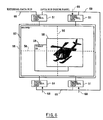
- a panel 55 that is the display screen is a high-resolution liquid crystal display panel of, for example, QUXGA (3200 x 2400 dots).
- the panel 55 is divided into four sub-panels by display dividing lines 56.
- the image developing onto these panels is driven by each of later described separate panel control chips 51. This is because in the actual panel 55 too many dots are to be processed and only one panel control chip 51 cannot drive the panel 55.
- One of the panel control chips 51 is connected to an external data bus 68, and each panel is connected to an intra-panel data bus 69.
- the external data bus 68 connected to the panel control chip 61 which is represented by dotted lines, is used for external input to each of the sub-panels from each system provided outside the display screen when a multi-system later described in an embodiment 2 is adopted.
- the window means an area which makes definite sense on an image space, of which the host is conscious, and a unit of a transfer processing of image data.
- a window 58 for displaying a three-dimensional (3D) moving picture screen and a window 59 used for a text display are illustrated.
- the size becomes one fourth since a resolution of a screen is usually 100 dpi. Therefore, in the text display, the text characters are displayed using a larger font having a four-hold size.
- the data is originally made by VGA (640 x 480 dots), and the 3D moving picture is displayed so as to have a 2.5-fold size vertically and horizontally, namely with 1600 x 1200 dots.
- Figs. 9(a) and 9(b) are explanatory views for explaining processing for each data and a data processing quantity.
- Fig. 9(a) shows a systematic view showing a data source and each constituent component for processing the data.
- pre-handlers 26 to be described later which correspond to respective applications, such as text data, 3D animation, 32-bit color image and a DVD, are provided in a pre-processor 20 in a graphics chip 11 on the host side.
- the image data from the pre-handler 26 passes through an I/F transceiver 15, and is transmitted out to the panel side via a digital I/F line 49.
- the image data is inputted to a later described post-handler 78 in the panel control chip 51 via an I/F receiver 53.
- the post-handler 78 is a processing unit in charge of processing one window, and processing for the window is executed by the post-handler 78.
- the image is displayed on the panel 55.
- Fig. 9(b) shows a state where the data band width is limited in the prior art in which image data is developed on a host side and the developed image data is transferred to a panel side.
- image data is developed in a graphics memory 212 by a graphics chip 211 on the host side.
- the image data passes through the I/F transceiver 15 and is transmitted to the panel side via a digital interface (I/F) line 220 at a refreshing timing on the panel side.
- the image data is transferred to a panel control chip 202 via the I/F receiver 53, and displayed on a panel (not shown).
- Processing of 3D animation as typified by, for example games, is practically performed at most with a VGA resolution. Such resolution is not satisfactory, and a further increase in processing capability is expected. Processing capability several ten times as much as the VGA resolution is required for processing a display screen having a resolution equal to a UXGA resolution or more, as refreshing data quantity for generating the screen for the panel 55 with a resolution of QUXGA (3200 x 2400 dots), 3200 x 2400 x 24 (8 bits for each of R, G and B) x 60 [Hz] x 2.5 3.45 [G byte/s] is required.
- QUXGA 2000 x 2400 dots
- the maximum processing capability is determined by the bus widths of the graphics chip 211, the graphics memory 212 and the panel control chip 202.
- 90 % of 2.3 [Gbyte/s] is the maximum capability that can be used. Accordingly, when the panel 55 is a high-resolution screen, it is very difficult to develop the memory processing chip.
- the number of the panel control chips 51 can be increased in accordance with the number of the sub-panels.
- the processing data quantity can be reduced to 1/4 for one panel control chip 51.
- the processing style required varies significantly depending on the display data. The whole of the display data is not processed in the same processing style, and if the display date is processed by the best processing style according to a sort thereof, the processing capability is greatly improved as a whole.
- the concept of the window is introduced in this embodiment.
- the data format is sorted, and the distributed processing is performed, thus solving the foregoing problems.
- a window for the 3D animation is generated with, for example, a VGA resolution, and its 2.5-fold enlarged display is performed.
- the SXGA screen showing a slow transfer speed of, for example, 30 [Hz] can be updated.
- the transfer speed between the graphics chip 211 and the graphics memory 212 must be about 3 [Gbyte/s].
- the transfer speed of 1.5 [Gbyte/s] is necessary for the digital I/F line 220, and four sets are necessary when a DVI interface is used.
- the half of the transfer speed of VGA and SXGA is satisfactory for the digital I/F line 49, and its transfer speed is 300 [Mbyte/s], which is 1/5 of that of the digital I/F line 220.
- the transfer speed between the panel control chip 51 and a panel memory to be described later on the panel side is 1 [Gbyte/s] or less, which is satisfactory.
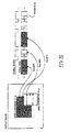
- Fig. 10 is an explanatory view for briefly explaining a transfer method of image data using a packet used in this embodiment, in conjunction with the foregoing window. It is now assumed that an area A and an area B exist as an image generated by an application on the host. In this embodiment, a developing operation of the image is not executed on the host side 10 to be described later, but executed on the panel side 50 to be described later. On the host side 10, a window ID: 4 is set for the area A and a window ID: 5 is set for the area B. The transfer of the image information to the panel side 50 is executed in a packet method in which the image information is sorted for each area.
- an image signal is transferred after, for example, packetizing of the image signal at each scan, in response to a Display Enable signal. ID information is added to each packetized image signal, and then the packetized image signal is transferred. If each handler to be described later in a specified sub-panel is set so as to process the window ID: 4 and the window ID: 5, the image information, which is transferred in the form of a packet and to which the window ID is added, can be developed on a specified panel. Note that the data transfer in the form of a packet will be described later in detail.
- Fig. 1 is a block diagram showing an embodiment of the image display system to which the present invention is applied.
- reference numeral 10 denotes a host side composed of a personal computer (PC and the like), which serves as a driver for driving the display device in this embodiment.
- reference numeral 11 denotes a graphics chip, and a pre-processing of the image data is executed by a pre-processor 20 built in the graphics chip 11.
- Reference numeral 12 denotes a graphics memory, which is constituted by a smaller capacity compared to conventional ones because the graphics chip 11 needs not perform continuous refreshing by a later described distributed processing.
- Reference numeral 13 denotes a system bus connected to a host system (not shown) for executing an application.
- Reference numeral 14 denotes a graphics memory bus arranged between the graphics chip 11 and the graphics memory 12. Furthermore, reference numeral 15 denotes an interface (I/F) transceiver, which serializes the image data and transmits the image data to the panel side 50 through the digital I/F line 49.
- I/F interface
- a plurality of panel control chips 51 are provided on the panel side 50.
- the divided panel 55 is driven by use of the four panel control chips 51.
- Reference numeral 52 denotes a panel memory provided in each panel control chip 51.
- Reference numeral 54 denotes a panel data outputted for transmitting the output from the panel control chip 51 to the panel 55.
- reference numeral 55 denotes a panel for actually displaying an image, and the panel 55 is divided into the four areas in Fig. 1.
- This panel 55 is constituted by a high-resolution panel, and to support this high-resolution screen, the panel control chip 51 makes it possible to perform plural parallel processings.
- reference numeral 68 denotes an external data bus
- reference numeral 69 denotes an intra-panel data bus.
- This embodiment has a feature in that the pre-processor 20 in the graphics chip 11 executes pre-processing of the data and the post-processor 70 in the panel control chip 51 executes post-processing.
- the job concerning the image generation is executed by the display device side (panel side 50), the job having been executed by the graphics chip 11 on the host side 10.
- a tag, an attribute of the image date and an error protection are added to the undeveloped image data by the pre-processor 20 or to the unmixed image data, in other words, and the post-processor 70 first develops the image data in the panel memory 52.
- the post-processor 70 uncompresses the image data and mixes, then the post-processor 70 transfers it to a refreshing circuit (not shown).
- the graphics chip 11 on the host side 10 performs reading/writing from/to the graphics memory 12 through the graphics memory bus 14.
- An application system (not shown) for executing an application is handled by use of the system bus 13.
- the foregoing AGP is adopted for the system bus 13. Although this AGP has performance doubled to eightfold that of the conventional PCI bus, the AGP is not a bus, only one AGP becomes active in the system.
- a digital output of the graphics chip 11 is sent to the I/F transceiver 15, and serialized and transferred with a high speed therefrom.
- the image data serialized by the I/F transceiver 15 is transmitted to the I/F receiver 53 on the reception side via the digital I/F line 49.
- This I/F receiver 53 converts the serialized image data back to the original parallel video data.
- the image data converted to the parallel data is transmitted to the panel control chip 51.
- the panel control chip 51 the image data packetized as described later is first uncompressed by the post-processor 70, and a window ID to be described later is recognized. A data operation in accordance with the window ID is performed, then the image data is developed and stored in the panel memory 52.
- the panel control chip 51 sequentially reads out the display data from the panel memory 52, and sends out the read-out display data to the panel 55.
- the greater part of the jobs concerning display processings are performed by the post-processor 70 and circuits located at the rear stage thereof, the jobs which including image data developing, refreshing for displaying, timing generation in the horizontal (H)/vertical (V) direction, allocation of memories depending on a screen size of the display device and allocation of the number of colors.
- These processings have heretofore been performed by the graphics chip 11.
- the graphics chip 11 because a load of the graphics chip 11 on the host side 10 is reduced and the display processing is performed by the panel control chip 51 which can be constituted by a multi-chip, the system of this embodiment is capable of functioning sufficiently as a technique for displaying a high-resolution display.
- the image data is simply processed, for example, with the VGA resolution, and processed so as to magnify it by the panel control chip 51. Accordingly, it is possible to display a moving picture such as 3D graphics.
- Fig. 2 is a view for explaining the graphics system on the host side 10 which was described in Fig. 1.
- a D/A converter hereinafter referred to as a DAC 16 and an address generator 17 for generating synchronized signals.
- the address generator 17 outputs the synchronized signals including H-Sync and V-Sync together with the display enable signal, as the form that can be immediately displayed in the display device.
- This embodiment is constituted such that processing to be executed by the graphics chip 11 is reduced, the image data is not developed and the undeveloped image data is transferred to the panel side. Color data composed of, for example, 24 bits is outputted to the pre-processor 20.
- a DE signal for indicating data valid that is, indicating that the data is sent, and an address signal for setting a start point, are outputted from the address generator 17 to the pre-processor 20.
- the pre-processor 20 executes processing for adding a window ID and address information to the image data.
- a 12C base interface known as Display Data Channel (DDC) is used for information exchange between the host side 10 and the panel side 50.
- DDC Display Data Channel
- Fig. 3 is a block diagram showing an internal structure of the pre-processor 20.
- An input latch 21 latches video data inputted from an application thereto.
- an ID register 22 a window ID to be added to the packet is set, and a pre-handler 26 corresponding to this window ID is selected.
- the pointer 23 converts simple information such as an address and an order of data.
- the sync bit 24 is a bit for making synchronization of the display screen with the writing data. A synchronization of a vertical counter of the display screen is made in response to this bit.
- the check bit generator 25 Upon receipt of data inputted from the input latch 21 and a Display Enable signal indicating data valid, the check bit generator 25 generates check bits of the image data including parity, sum and CRC.
- the pre-handler 26 is a handler on the pre-processor 20 side, and has data for each window ID.
- the handler means a processing unit in charge of processing one window, and is provided also in the post-processor 70 on the panel side 50, to be described later.
- the handler has various kinds of registers.
- a window ID register 27 shows an ID indicating to which window each handler in the pre-handler 26 corresponds.
- a clip register 28 is a register indicating an actually writable area.
- a position register 29 indicates a position of the transfer data.
- a scale register 30 is a register indicating a magnifying power for scaling the image data.
- a mode register 31 indicates a transfer mode and a writing mode of the image data.
- a priority register 32 indicates a priority for each window ID.
- a DDC handler 37 transmits/receives a control signal of DDC between the host side 10 and the panel side 50.
- a job number output register 33 is a register for writing the job number, and the job number is transmitted to the panel side 50 via the DDC handler 37.
- a job number input register 34 the smallest job number in all is read thereinto via the DDC.
- the job number is used for making synchronization when a multi-system constitution is adopted as is described in a later described second embodiment.
- a sync back register 35 is used for making synchronization with the panel side 50, and is constituted such that normalized vertical information of the panel side 50 can be read.
- An error status register 36 is constituted such that error information processed on the panel side 50 is returned to the host side 10.
- a muliplexer 38 multiplexes header information from the ID register 22, the pointer 23 and the sync bit 24, body information that is video image data from the input latch 21, footer information from the check bit generator 25 and a command from the pre-handler 26, and packetizes them to transfer them to the panel side 50.
- Fig. 4 is a block diagram showing a schematic constitution of a display circuit on the panel side 50.
- the panel control chip 51 comprises a post-processor 70, an input first-in-first-out memory (FIFO) 61, an output FIFO 62, an input address register 63, and an output register 64 having an H counter 65 and a V counter 66.
- the image data which is serialized and transferred from the host side 10 is converted to parallel image data and a control signal DE by the I/F receiver 53.
- the data from the I/F receiver 53 adopts the form of packet unlike the prior art, and is uncompressed and processed by the post-processor 70.
- the post-processor 70 is provided within the panel control chip 51 on the panel side 50, and processes the packet transmitted from the host side 10.
- Processing such as scaling is one of the processings executed by the post-processor 70.
- the image data is read out from the panel memory 52 and written thereto while timing its reading-out and writing by the input FIFO 61 and the output FIFO 62, and then transmitted to a next processing.
- the image data processed by the post-processor 70 is X/Y address, and is converted to memory address by the input address register 63.
- the memory address which is converted from the image data is inputted to the panel memory 52 and the output address register 64.
- the output address register 64 comprises the H counter 65 and the V counter 66, and outputs synchronized signals in the horizontal/vertical directions to the panel 55. Conversion of the display mode is executed by the post-processor 70.
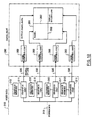
- Fig. 5 is a block diagram showing an internal constitution of the post-processor 70.
- An input latch 71 latches packet data inputted thereto.
- a window ID stored in the packet is set in an ID register 72.
- a pointer 73 converts simple information such as packetized addresses and information relating to data order.
- a sync bit 74 is a bit for making synchronization of the display screen with writing data. Synchronization of the vertical counter for the display screen is made in response to this bit.
- An error generator 75 detects a data error based on check bits of the data.
- an address generator 76 generates addresses from pointers and packet information from the ID register 72, the pointer 73 and the sync bit 74.
- a clipping circuit 77 is constituted to detect a writable area from the clip register 80 in the post-handler 78 and the priority control circuit 89, and to cut out data of that portion for the image data from the input latch 71.
- the post-handler 78 is a handler on the post-processor 70, and functions as a processing unit in charge of processing the window.
- a window ID register 79 in the post-handler 78 indicates a window ID of a packet to be processed by each handler in the post-handler 78.
- the clip register 80 is a register indicating an actually writable area.
- a position register 81 indicates a position of the transfer data.
- a scale register 82 is a register indicating a magnifying power for scaling the image data.
- a mode register 83 indicates a transfer mode for the image data and a writing mode for the image data.
- a priority register 84 indicates a priority of a clip area of each handler.
- An error status register 85 is a register showing an error status in processing on the panel side 50.
- a DDC controller 86 executes processing of a DDC control signal transmitted/received between the host side 10 and the panel side 50.
- the scaling circuit 87 the image data outputted from the clipping circuit 77 is magnified and reduced, and outputted to the panel 55.
- a FIFO memory 88 is a memory used for magnifying/reducing the image data in the scaling circuit 87.
- a priority control circuit 89 sets a writable area of the image data for the window ID based on a processing area (clipping area) of the respective post-handler 78 and each priority.
- a synchronization control circuit 90 is a circuit which uses the normalized vertical counter and is used for making a vertical synchronization of the panel and for a synchronization of data processing. The synchronization control circuit 90 outputs a vertically synchronized signal.
- a job number register 91 is connected to an internal bus that is a low speed bus, and is used when a multi-system is adopted. The job number register 91 stores the smallest
- each register of the pre-handler 26 in the pre-processor 20 is set in accordance with a window by an application (step 301). This information is transferred to the post-processor 70 via the DDC handler 37 by the DDC control signal, and the window ID register 79 of the post-handler 78 is set (step 302). On the other hand, the ID register 22, the pointer 23 and the sync bit 24 are written as header information of a packet, which is used when the image data is transferred (step 303). Furthermore, the pre-processor 20 transfers information of the post-handler 78 in the form of a packet after allowing the information of the post-handler 78 to be included in a body of the packet (step 304). The transferred data is stored in the post-handler 78 having the same ID as the transferred data (step 305).
- the video data is inputted to the packet body, and the video data is transferred from the system in the form of header-body-footer (step 306).
- the panel side 50 first cuts out the header from the packet, and then selects the post-handler 78 corresponding to ID in the header. Processing is executed by the selected handler (step 307). A data portion is processed based on clip information, and its priority, position information and address information of the header. Thereafter, data and an address are sent to the next stage (step 308). At the same time, an error detection is executed, and error information is stored (step 309).
- step 306 to step 309 are executed for each line (for example, 1280 dots) or for each block (for example, a block of 32 x 32 dots) (step 310).
- Error information is read from the system on the host side 10 via the DDC, periodically, and a necessary processing such as transfer stop and re-transfer is performed (step 311).
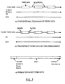
- Figs. 7(a), 7(b) and 7(c) are explanatory views showing a comparison of a data transfer of the prior art with that of this embodiment, and a data format.
- Fig. 7(a) shows a conventional transfer of video data.
- video data of R(Red), G(Green) and B(Blue), V-sync, H-sync, DE and other about two control signals are serially sent out.
- the video data is sequentially transferred one line by one line from upper left to lower right in accordance with the display screen. Furthermore, during the data transfer, a period in which no data is transferred exists as a blanking time.
- a transfer of video data in this embodiment shown in Fig. 7(b) utilizes a blanking time in the conventional transfer.
- Information of 16 dots or less is added to the header and the footer. This is called packetization. Since packets from a plurality of sources are dealt with in this embodiment, a synchronized signal of V-sync and H-sync does not make sense, so that the V-sync information is included in the header. Accordingly, one DE that is a signal indicating a quantity of data transfer is satisfactorily used as the synchronized signal. This synchronized signal is used for error processing in this embodiment. A quantity of information processed by the DDC increases, and bidirectional use is adopted. Furthermore, the quantity of data is not invariable.
- data format is considered so as to make it similar to that of the prior art. This is because in consideration of the case where the conventional PCs and the conventional monitoring apparatus are placed on the market, to keep compatibility of the appliance of this embodiment with that adopting the conventional system is intended. To minimize the change of the graphics chip, this embodiment is considered so as to be able to be supported without changing the data format so much.
- the data format in this embodiment is shown in Fig. 7(c).
- the body is an ordinary image data portion, and variable in length.
- the header portion includes a window ID corresponding to a name tag of the image data, a pointer indicating a write position, and a synchronous bit in lieu of V-sync.
- a footer exists in the final packet bit, and is used for the error detection. This is because since data is transmitted via a transmission system, the case where a phase error may occur is considered.
- the screen refresh work it is possible to move the screen refresh work toward the display device side (panel side 50) and reduce the work load by scaling the image data in the display device.
- a window display is performed in the ultra-high-resolution panel, characters and the like must be naturally displayed with a high resolution, and they must be displayed with a high resolution also in the case of a still picture.
- a screen with VGA resolution is displayed, for example. According to this embodiment, by separating these two portions, the portion of the still picture is refreshed using a memory on the panel side 50.
- the system side (host side 10) performs only the 3D work, processing capability can be increased to be double with respect to, for example, SXGA.
- the display of the 3D display portion with a resolution of VGA (640 x 480 dots) and at a size of XGA (1024 x 768 dots)
- data transfer has been heretofore performed after scaling up the image data to about 1.5 times on the system side.
- image data is magnified by four times with a ultra-high-resolution, and under strict conditions relating to power consumption charged on, for example, notebook type personal computers, such idea is particularly a large merit.
- the display processing of moving pictures by the multi-system in this embodiment has roughly two features.
- each system controls the corresponding one of the screens divided, but also one system can control the whole of the screen.
- the OS of one system can control only 1/4 of the whole of the screen, but cannot control the whole of the screen.
- one system can perform an ordinary window processing. At the same time, such a constitution is possible in that only for a specified 3D window, a support is made by a plurality of systems.
- the other feature is the difference in the ways how to get synchronization.
- the system had a high speed LA and a special communication means, and the plurality of systems heretofore has been synchronized with each other by the high speed LA and the communication means.
- this method has been complicated, and highly interdependent among the systems.
- Fig. 11 is a block diagram for explaining a system constitution of the multi-system in this embodiment.
- the panel 55 is divided into four parts by the display dividing lines 56, and the four parts are connected to the respective panel control chips 51.
- the panel 55 is divided into four parts by the display dividing lines 56, and the four parts are connected to the respective panel control chips 51.
- the respective panel control chips 51 there is not always necessary to provide a plurality of panel control chips 51, but it is possible to constitute the multi-system so that the panel 55 is controlled by one control panel.
- video data is sent from the corresponding graphics chip 11 in different systems 100.
- the panel control chips 51 are connected to each other by the intra-panel data bust 69 so that one system 100 can simultaneously control the whole of the screen.
- the screen refresh has one timing, as a matter of course, and each system must be synchronized with this timing of the screen refresh. For example, suppose that a person is displayed on the upper and lower screens, and refreshing data is rewritten supposing that the person is moving toward the right. If each system is not synchronized with the timing of the screen refresh, phenomenon in which only the upper portion moves toward the right by one dot and the lower portion is left as it is will occur, on the display dividing line 56 that is the seam of the screens.
- the other is the problem of synchronization of moving picture processing itself.
- Such problems occur when an application of the moving picture is not controlled by time.
- a work load to be processed during 16 [msec] that is one frame is not decided, but a display frame is advanced in accordance with performance of the system or the screen is more finely displayed.
- image data transmitted from these systems is joined and displayed, the data quantity processed in each of the screens is different, so that phenomenon may occur in which the left side screen performs processing quickly and performs an image processing such as fogging, and the right side screen performs processing slowly and does not perform the image processing such as fogging.
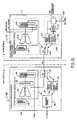
- Fig. 12 is an explanatory view showing a constitution for performing a synchronization processing between the host side 10 and the panel side 50 in this embodiment.
- the above described two problems concerning synchronization are solved by use of a DDC signal.
- the pre-processor 20 in the graphics chip 11 comprises a synchronization control circuit 40, a read/write control 45 and the like.
- the synchronization control circuit 40 comprises an offset register 41, an adder 42, a multiplexer 43 and a vertical synchronization counter 44.
- the post-processor 70 of the panel control chip 51 on the panel side 50 comprises a synchronization control circuit 111, a DDC handler 115 and job number controller 116.
- the synchronization control circuit 111 comprises a vertical synchronization counter 112, an offset register 113 and adder 114.
- the job number controller 116 comprises a job number input register 117, a job number output register 118, a comparator 119, an internal bus controller 120 and an internal bus 121.
- a vertical synchronization counter 112 having position information of the screen refresh is provided on the panel side 50.
- all chips have the same value by two internal synchronization signals (INT#VSYNC and INT#HSYNC). However, when only one panel control chip 51 is provided, this is not required.
- An output from the offset register 113 is added to the adder 114 for each INT#HSYNC, and normalized so as not to be affected by the number of vertical lines of the panel 55. This value is read out by the DDC, and written to the vertical synchronization counter 44 in the graphics chip 11 on the system side 100.
- the output from the vertical synchronization counter 44 is added to the adder 42 together with the output from the offset register 41.
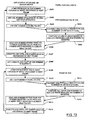
- Fig. 13 is a diagram showing a process flow in this embodiment.
- the left hand of Fig. 13 shows a processing flow of an application of the system 100 or on the device driver side.
- the right hand of Fig. 13 shows a processing flow in the panel control chip 51 on the panel side 50.
- This embodiment is constituted such that a work from each system 100 is managed by a job, and the multi-system composed of the plurality of systems 100 can share the drawing of an image.
- the job (task) is a division unit to define the extent of image to be drawn, defining to which polygon (triangular shape in 3D) the image is drawn in the case of a moving picture, for example, and a job (task) number is given to divided image processing by an arbitrary unit and is expressed by sequence number.
- a unit of the image processing is arbitrarily selectable, and since processing in one frame is delimited, there is no problem when image processing is delimited to several ten or more units.
- the application computes the maximum job number of processing which can be executed in a next frame at a certain timing (step 401). Further, to execute synchronization of the job, the job number of the master PC serving as a master in the plurality of systems 100 is set to zero (or minimum) and an operation is stopped (step 402). The maximum job number computed is transferred to the panel control chip 51 on the panel side 50 via the DDC.
- the image processing presupposes that it is split up into a specified unit, and numbered in the processing order.
- Each panel control chip 51 passes the respective job number sequentially to the internal bus (INT#BUS) 121 on the panel side 50 (step 404).
- the value of the job number on the bus is compared with others by the comparator 119, and the smaller job number than others is read.
- the smaller number read is written to the job number output register 118 (step 405).
- the job number is read via the DDC, and the job number is read from the job number output register 118 of the panel control chip 51 or the job number input register 34 already read (step 406).
- jobs until the job number read are executed as a processing in a next frame, based on the job number read (step 407).
- the master PC sets the job number to zero, and thus a startup of each application is stopped. The operation is started when the master PC starts to operate, and each system 100 can acquire the job number to be processed by the application. A series of processing is executed until a correct job number is set to the master PC, and thus synchronization of the jobs with each other in the plurality of systems 100 is performed.
- the processing flow can achieve the synchronization with the slowest system 100 in the plurality of systems 100.
- the correct number is set to the master PC (step 408).
- the job starts.
- the maximum job number that can be processed in a next frame is computed (step 409).
- the job number is set with respect to the panel 55 via the DDC (step 410).
- each panel control chip 51 passes the respective job number sequentially to the internal bus (INT#BUS) 121 on the panel side 50 (step 411).
- the value of the job number on the bus is compared with others, and the smaller job number than others is read.
- the smaller job number is written to the job number output register 118 (step 412).
- the job number is read via the DDC, and the job number is read from the job number output register 118 of the panel control chip 51 and the job number input register 34 already read (step 413).
- jobs are executed as a processing in a next frame until the job number read, based on the job number read (step 414). Thereafter, the procedure returns to step 409.
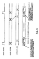
- Fig. 14 is a timing chart for further explaining the synchronization processing operation by the multi-system, which was explained by the foregoing flowchart.
- the panel vertical counter Panel V-CNTR
- V-SYNC vertical synchronization
- This register is read at a certain time point, and the value of the register is written to the vertical synchronization counter 44 on the system side 100.
- a little delay takes place in writing to the vertical synchronization counter 44. It is possible for the system side 100 to recognize the synchronization after waiting for this delay.
- the vertical synchronization counter 44 of the system 100 uses the timing close to the maximum value, and each starts to compute the job number.
- the vertical counter (VCNTR) starts the processing after passage of (N + X) time.
- the data transfer from a double buffer (not shown) of the system side 100 to the panel side 50 is begun.
- the counted value is written to the job number input register 117 on the panel side 50.
- the value of each panel control chip 51 is loaded on the internal bus 121 at a suitable timing.
- Each panel control chip 51 reads the value to be loaded on the internal bus 121 from the internal bus controller 120.
- the value of the job number input register 117 and the value written to the job number output register 118 are compared with each other, and the smallest value is obtained from the comparator 119. The smallest value obtained is written to the job number output register 118 again.
- the system 100 which read the smallest value of the job number executes the job having the smallest job number in the next processing, and, at the same time, performs the setting of the vertical counter (V-CNTR).
- the job number and the value of the vertical counter (V-CNTR) are read via the DDC.
- the job number for processing a next frame is determined, and, at the same time, the vertical counter (V-CNTR) is set.
- the present invention even in the case of the 3D display in which the power on the system side is lacking, it is possible to perform the display, for example, by dividing the display portion into four parts.
- the divided four parts are driven by the four systems, respectively, it is possible to display a large screen having a size nearly equal to SXGA (1280 x 1024 dots), which is the quadruple of the divided four parts, and showing a ultra-high-resolution of 10"UXGA (200dpi).
- SXGA 1280 x 1024 dots
- 10"UXGA 200dpi
- plural kinds of systems that is, PCs loading entirely different OSs, can display the respective screens, and display the screen cooperatively.
- the support of the displayed colors of 24 bits or more has been heretofore limited to a high-end work station.
- One factor of such limitation is that the system becomes expensive due to an increase in a processing speed for each portion to support the display colors of 24 bits or more.
- this embodiment by executing the distributed processing by the host side and the system side, it is possible to slow the processing speed of the system, and it is made easy to support the display colors of 24 bits or more.
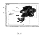
- Fig. 15 shows a state where a color image and a monochrome image are mixedly displayed on the display screen.
- the window 58 of a 3D moving picture screen and the window 130 of a monochrome image are displayed in addition to the window 59 composed of an ordinary text screen.
- the window 58 of the 3D moving picture screen is a color screen of 30 bits
- the window 130 of the monochrome image is a unicolor screen. It is possible to display the images of different types mixedly on the panel 55 which was described in the embodiments 1 and 2.
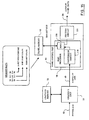
- Fig. 16 is a diagram for explaining a control flow and a block constitution which execute processing in this embodiment.
- the panel control chip 51 has a FRC/dither circuit 131 for enhancing a gradation for display.
- the conversion circuit 132 for performing gamma adjustment and processing of color matching and the FIFO buffer 133 for adjusting timing of reading/writing from/to the panel memory 52 are provided.
- Image data of 32 bits sent from an application of the system is inputted to the graphics chip 11 via the system bus 13.
- the image data is processed by the graphics chip 11, and sent to the panel control chip 51 via the digital I/F line 49.
- the image data is transferred as 24 bit data by use of a data format to be described later.
- the image data sent via the digital I/F line is converted to 30 bit data again by the post-processor 70, and written to the panel memory 52.
- the image data takes the form in which red (R), green (G) and blue (B) are respectively 10 bits as shown in the memory data format of Fig. 16.
- the image data read into the FRC/dither circuit 131 is converted to 8 bit data for each of R, G and B, and transferred to an X-driver (not shown) of the panel 55 from the panel data output 54.
- the FRC/dither circuit 131 functions so as to enhance a gradation display for R data, G data and B data by means of temporal distribution and spatial distribution.
- Figs. 17(a) and 17(b) show a data format example by the digital I/F line 49.
- Fig. 17(a) shows a Transition Minimized Differential Signaling (TMDS) data transfer.
- Fig. 17(b) shows bit assign of 30 bit color using the TMDS.
- the three TMDSO to the TMDS2 shown in Fig. 17(a) correspond to the three signals other than clocks, and perform coding from R data of 8 bit, G data of 8 bits and B data of 8 bits to R data of 10 bits, G data of 10 bits and B data of 10 bits, respectively, and transfer them.
- R data of 8 bit, G data of 8 bits and B data of 8 bits correspond to the three signals other than clocks, and perform coding from R data of 8 bit, G data of 8 bits and B data of 8 bits to R data of 10 bits, G data of 10 bits and B data of 10 bits, respectively, and transfer them.
- data for each one dot is illustrated vertically as a matter of convenience, coded
- a data transfer mode can be specified in the header of the packet, and data processing is performed in accordance with the specified transfer mode.
- two control bits are actually added to each dot in the 30 bit transfer, and these two bits are assigned dynamically in the data transfer mode.
- data transfer mode is used, as Write-per-bit (a mode in which a portion showing ON of the bit is written) and vertical parity bit, by strengthening error check of the data.
- write-per-bit a mode in which a portion showing ON of the bit is written
- vertical parity bit by strengthening error check of the data.
- This 30 bit data has a constitution in that high order 6 bits of monochrome are shared by R, G and B, and low order 6 bits are allocated (8 bits x 3) to gamma adjustment and color matching for each R, G and B, respectively, making 30 bits in total.
- One bit is added for an identification bit, thus 31 bits are written to the panel memory 52.
- the bits in which the identification bit is ON perform monochrome processing, and the bits in which the identification bit is OFF performs the ordinary color processing.
- Fig. 16 shows an example of these memory data formats.
- R8/G8/B8 is 8 bit color data
- R10/G10/B10 is 10 bit color data
- R8/G14/B8 is 14 bit monochrome data.
- 6 bits from 14 bits of G are the above described shared bits.
- processing to be executed subsequently is changed in accordance with the identification bit written to the panel memory 52 in the above described manner.
- the identification bit With reference to the image data read out from the panel memory, it is decided by the identification bit whether or not the image data is monochrome. If the image data is monochrome, the low order 8 bits are added to the high order 6 bits shared by R/G/B, and 6 bits are converted to 8 bits of R/G/B by the FRC/dither circuit 131. Then, the converted 8 bits are transferred to the X-driver of the panel 55.
- this identification bit can be used for the processing such as gamma adjustment, color matching and scaling.
- the number of displayed colors is increased, a transfer speed of the image data can be varied freely, and a transfer format of the image data is constituted freely.
- the processing such as the gamma adjustment and the color matching can be executed on the system side and the panel side without any problem.
- such processing is executed on both of the system side, and the image data can be transferred in a 30 bit color mode.
- the panel side has a conversion table, and the data transferred to the panel side in a 24 bit color mode can be converted to 30 bit color by a selection table.
- identification bit for deciding whether the data is color or monochrome is used, release from processing R/G/B individually is brought about.
- a monochrome image composed of multi-bit such as 14 bits
- an application to an X-ray display in which monochrome showing a multi-gradation is required is possible.
- a partial display of a screen of Digital Versatile Disc (DVD) is enumerated.
- Original DVD data is compressed, and the compressed DVD data must be uncompressed by the system and the graphics chip in the past. On the contrary, if the compressed portion is separated and data as compressed can be transferred, a transfer quantity is greatly reduced.
- the ultra-high-resolution image data of which dots are invisible is to be outputted, the ultra-high-resolution image data can be displayed without any deterioration of performance of the whole of the system such as lacking in capacity and a delay of a processing speed.
- the present invention it is possible to achieve the distributed processing on the host side and the panel side (monitor side), and a work load of the whole of the system including the graphics chip can be optimized.
- the processing capability of the image display system including the transfer capability can be exhibited sufficiently, and the problem such as lack in the display capability on the ultra-high-resolution panel and the multi-panel can be solved.
Landscapes
- Engineering & Computer Science (AREA)
- Theoretical Computer Science (AREA)
- Physics & Mathematics (AREA)
- General Physics & Mathematics (AREA)
- Computer Hardware Design (AREA)
- Multimedia (AREA)
- Human Computer Interaction (AREA)
- General Engineering & Computer Science (AREA)
- Signal Processing (AREA)
- Controls And Circuits For Display Device (AREA)
- Control Of Indicators Other Than Cathode Ray Tubes (AREA)
Abstract
Description
Claims (11)
- An image display system comprising:a host for executing an application; anda display connected to the host, the display displaying an image,wherein said host transfers undeveloped image data to the display when the host requests the display to display the image; andsaid display includes a panel memory for developing the image, develops the image in the panel memory based on the image data transferred from said host, and displays the image on its panel, which is developed in the panel memory.
- An image display system comprising:a plurality of system devices for executing the same application; anda display device having panel controlling means for dividing a display area into a plurality of areas and controlling driving of the divided areas,wherein the plurality of system devices are connected to respective panel control means provided in said display device, and output first control signals for a synchronization with said display device to the respective panel control means; andsaid panel control means in said display device outputs a second control signals for a synchronization with said display device to the system devices, based on the first control signals outputted from said plurality of system devices.
- An image display system comprising:a host for executing a plurality of applications showing different display characteristics and data quantities, which are required;a display for displaying an image; anda digital interface for transferring image data from said host to said display,wherein said digital interface changes a transfer format depending on an application executed by said host, and transfers image data to said display; andsaid display develops said image data transferred via said digital interface in a panel memory for developing, and then displays an image on a panel.
- A host device comprising:executing means for executing a plurality of applications having different display characteristics and data quantities, which are required;window managing means for managing a window ID defined for a window that is an area which makes definite sense in an image space, of which said application is conscious; andimage data transfer means for adding the window ID managed by said window managing means to undeveloped image data, for which said application requests a display, and transferring the undeveloped image data.
- A host device comprising:image transfer means for transferring image data to a display connected thereto; andcontrol means for supplying image data to said data transfer means based on an executed application of a still picture and an executed application of a moving picture,wherein said control means supplies the image data regardless of refresh timing required for said display with respect to the application of said still picture, and supplies the image data in synchronization with refresh timing required for said display with respect to the application of said moving picture.
- An image display device comprising:a panel for displaying an image;image data receiving means for receiving undeveloped image data from a host device which executes an application;a panel memory for developing said image data received from said image data receiving means; andpanel control means for developing image data for said panel memory and writing a developed image for said panel.
- An image display device which is connected to a plurality of system devices for executing the same job, and displays an image based on image data transferred from the plurality of system devices, comprising:a display section for displaying the image, either as panels divided into a plurality of display areas or as one panel obtained by collecting a plurality of display panels; andone or more panel control means for controlling an image display of said display section,wherein said panel control means receives a control signal concerning a job from said plurality of system devices, and transmits a control signal used for achieving synchronization of the system devices to said plurality of system devices.
- An image display device comprising:a panel for displaying an image;image data receiving means for receiving undeveloped image data from a host side which executes a plurality of applications;a panel memory for developing said image data received from said image data receiving means; andpanel control means for developing image data for said panel memory and performing a color adjustment for each image data, each image data transferred by one of said different applications, thus writing an image to said panel.
- An image display device comprising:a panel for displaying an image;image data receiving means for receiving color image data of the first number of bits and monochrome image data of the second number of bits different from the first number of bits from a host side;a panel memory for developing said image data received from said image data receiving means; andpanel control means for developing image data for said panel memory,wherein said panel control means develops said color image data and said monochrome image data, which are received from said image data receiving means, in said panel memory, the color image data and said monochrome image data being developed in different data formats.
- An image display method for displaying an image on a display connected to a host, based on a signal from the host which executes an application, comprising the steps of:transferring undeveloped image data for an image display from said host to said display via a digital interface;developing said transferred image data by said display itself, for a memory of said display; anddisplaying an image developed in said memory on said display.
- An image display method for displaying an image on a display connected to a host, based on a signal from the host which executes an application, comprising the steps of:transferring image data showing a first resolution executed by said application from said host to said display;scaling the image data showing the first resolution by said display, which is transferred from said host;developing an image with a second resolution different from said first resolution; andoutputting the image to a panel of said display so as to display the image on the panel.
Applications Claiming Priority (2)
| Application Number | Priority Date | Filing Date | Title |
|---|---|---|---|
| JP34146199 | 1999-11-30 | ||
| JP34146199A JP3526019B2 (en) | 1999-11-30 | 1999-11-30 | Image display system, image display device, and image display method |
Publications (2)
| Publication Number | Publication Date |
|---|---|
| EP1107224A2 true EP1107224A2 (en) | 2001-06-13 |
| EP1107224A3 EP1107224A3 (en) | 2008-03-26 |
Family
ID=18346255
Family Applications (1)
| Application Number | Title | Priority Date | Filing Date |
|---|---|---|---|
| EP00310577A Withdrawn EP1107224A3 (en) | 1999-11-30 | 2000-11-29 | Image display system and method comprising a host device and an image display device |
Country Status (7)
| Country | Link |
|---|---|
| US (2) | US20010002124A1 (en) |
| EP (1) | EP1107224A3 (en) |
| JP (1) | JP3526019B2 (en) |
| KR (1) | KR100383751B1 (en) |
| CN (1) | CN1182469C (en) |
| CA (1) | CA2323995A1 (en) |
| TW (1) | TW487900B (en) |
Cited By (8)
| Publication number | Priority date | Publication date | Assignee | Title |
|---|---|---|---|---|
| WO2002071380A3 (en) * | 2001-03-06 | 2003-09-18 | Ibm | Image display system |
| WO2006075879A1 (en) * | 2005-01-12 | 2006-07-20 | Samsung Electronics Co., Ltd. | Host device, display device and display system |
| WO2009024523A1 (en) * | 2007-08-23 | 2009-02-26 | Seereal Technologies S.A. | Electronic display unit and device for actuating pixels of a display |
| EP2040245A1 (en) * | 2007-11-27 | 2009-03-25 | Samsung Electronics Co., Ltd. | Display apparatus and control method thereof |
| EP2129106A1 (en) * | 2008-05-09 | 2009-12-02 | Nexcom International Co. Ltd. | Method and system for processing video signals |
| EP1632844A3 (en) * | 2004-09-07 | 2010-07-28 | Samsung Electronics Co., Ltd. | Apparatus for and method of generating graphic data, and information recording medium |
| EP2131275A3 (en) * | 2008-05-09 | 2010-12-29 | Nexcom International Co. Ltd. | Video control system, display system control device and video controlling method for e.g. video wall |
| US8866915B2 (en) | 2005-11-15 | 2014-10-21 | Lawrence Livermore National Security, Llc | High speed, real-time, camera bandwidth converter |
Families Citing this family (64)
| Publication number | Priority date | Publication date | Assignee | Title |
|---|---|---|---|---|
| JP2002116729A (en) | 2000-10-04 | 2002-04-19 | Internatl Business Mach Corp <Ibm> | Data processing method, picture display method, picture processing device, picture display device, picture display system, and picture processing system |
| JP2002323876A (en) * | 2001-04-24 | 2002-11-08 | Nec Corp | Picture display method in liquid crystal display and liquid crystal display device |
| KR100471062B1 (en) * | 2001-12-08 | 2005-03-08 | 삼성전자주식회사 | Lcd monitor with dualinterface and control method thereof |
| JP4300001B2 (en) * | 2002-07-31 | 2009-07-22 | ソニー株式会社 | Clipping device |
| JP3942986B2 (en) | 2002-08-09 | 2007-07-11 | Necディスプレイソリューションズ株式会社 | Display device, display system and cable |
| JP3945355B2 (en) * | 2002-09-11 | 2007-07-18 | ソニー株式会社 | Video display device |
| JP2004219759A (en) * | 2003-01-15 | 2004-08-05 | Chi Mei Electronics Corp | Image display processing method, image display processing apparatus, image display device, and image display processing system |
| US7091980B2 (en) * | 2003-08-28 | 2006-08-15 | Evans & Sutherland Computer Corporation | System and method for communicating digital display data and auxiliary processing data within a computer graphics system |
| JP2005348170A (en) * | 2004-06-03 | 2005-12-15 | Ricoh Co Ltd | Image reading apparatus, image processing apparatus, image forming apparatus, image processing method, computer program, and recording medium |
| JP4468238B2 (en) | 2004-07-12 | 2010-05-26 | シャープ株式会社 | Display device and driving method thereof |
| JP3792238B2 (en) * | 2004-07-16 | 2006-07-05 | シャープ株式会社 | Video signal line driving circuit and display device including the same |
| US8022894B2 (en) * | 2004-08-30 | 2011-09-20 | Mitsubishi Electric Corporation | Screen synchronous control apparatus |
| KR100710301B1 (en) * | 2005-01-14 | 2007-04-23 | 엘지전자 주식회사 | Multi-screen system and its implementation |
| JP2006268260A (en) | 2005-03-23 | 2006-10-05 | Seiko Epson Corp | Data transfer control device and electronic device |
| US20060227809A1 (en) * | 2005-03-23 | 2006-10-12 | Miller Rodney D | System and method for base band-directional communication protocol for time-division multiplexing graphic data applications |
| US7456833B1 (en) * | 2005-06-15 | 2008-11-25 | Nvidia Corporation | Graphical representation of load balancing and overlap |
| US8209620B2 (en) * | 2006-01-31 | 2012-06-26 | Accenture Global Services Limited | System for storage and navigation of application states and interactions |
| US20070115270A1 (en) * | 2005-11-23 | 2007-05-24 | Rai Barinder S | Image manipulation apparatus |
| JP4810214B2 (en) * | 2005-12-13 | 2011-11-09 | キヤノン株式会社 | VIDEO DISTRIBUTION DEVICE, VIDEO DISTRIBUTION METHOD, VIDEO DISPLAY METHOD, AND COMPUTER PROGRAM |
| JP4907220B2 (en) * | 2006-04-27 | 2012-03-28 | 三菱電機株式会社 | Large screen display system and multicaster |
| CN101617354A (en) | 2006-12-12 | 2009-12-30 | 埃文斯和萨瑟兰计算机公司 | Be used for calibrating the system and method for the rgb light of single modulator projector |
| US8451279B2 (en) | 2006-12-13 | 2013-05-28 | Nvidia Corporation | System, method and computer program product for adjusting a refresh rate of a display |
| JP2008178075A (en) * | 2006-12-18 | 2008-07-31 | Sony Corp | Display control apparatus, display control method, and program |
| KR101308295B1 (en) | 2007-04-12 | 2013-09-17 | 엘지디스플레이 주식회사 | Display device and driving method thereof |
| KR101467935B1 (en) * | 2007-12-11 | 2014-12-03 | 삼성전자주식회사 | Display device and control method thereof |
| WO2009086316A1 (en) * | 2007-12-21 | 2009-07-09 | Citrix Systems, Inc. | Systems and methods for efficient processing of data displayed by a window |
| US7907142B2 (en) * | 2008-01-15 | 2011-03-15 | Verint Systems Inc. | Video tiling using multiple digital signal processors |
| US8610727B1 (en) * | 2008-03-14 | 2013-12-17 | Marvell International Ltd. | Dynamic processing core selection for pre- and post-processing of multimedia workloads |
| US8358317B2 (en) | 2008-05-23 | 2013-01-22 | Evans & Sutherland Computer Corporation | System and method for displaying a planar image on a curved surface |
| US8702248B1 (en) | 2008-06-11 | 2014-04-22 | Evans & Sutherland Computer Corporation | Projection method for reducing interpixel gaps on a viewing surface |
| KR100973561B1 (en) * | 2008-06-25 | 2010-08-03 | 삼성전자주식회사 | Display |
| US8077378B1 (en) | 2008-11-12 | 2011-12-13 | Evans & Sutherland Computer Corporation | Calibration system and method for light modulation device |
| JP5578400B2 (en) | 2009-07-16 | 2014-08-27 | Nltテクノロジー株式会社 | Image display device and driving method used for the image display device |
| US8674935B2 (en) * | 2009-10-21 | 2014-03-18 | Qualcomm Incorporated | System delay mitigation in interactive systems |
| US20110148934A1 (en) * | 2009-12-18 | 2011-06-23 | Nokia Corporation | Method and Apparatus for Adjusting Position of an Information Item |
| US8963797B2 (en) | 2010-01-06 | 2015-02-24 | Apple Inc. | Display driving architectures |
| JP5210348B2 (en) * | 2010-04-23 | 2013-06-12 | 株式会社ナナオ | Image display device, image region detection method, and computer program |
| US20120033036A1 (en) * | 2010-08-04 | 2012-02-09 | Disney Enterprises, Inc. | System and method for displaying three-dimensional video |
| JP6070544B2 (en) * | 2011-04-28 | 2017-02-01 | 株式会社ソシオネクスト | Video display device and video display method |
| US9641826B1 (en) | 2011-10-06 | 2017-05-02 | Evans & Sutherland Computer Corporation | System and method for displaying distant 3-D stereo on a dome surface |
| JP6027739B2 (en) * | 2011-12-15 | 2016-11-16 | キヤノン株式会社 | Video processing apparatus, video processing method, video processing system, and program |
| WO2013105347A1 (en) * | 2012-01-10 | 2013-07-18 | ソニー株式会社 | Display device and display method |
| KR20130088686A (en) * | 2012-01-31 | 2013-08-08 | 삼성전자주식회사 | Display apparatus, display panel and method thereof |
| JP5486700B2 (en) * | 2013-01-23 | 2014-05-07 | Eizo株式会社 | Image display device, image region detection method, and computer program |
| TWI523516B (en) * | 2013-04-11 | 2016-02-21 | 威盛電子股份有限公司 | Video wall |
| CN103730097B (en) * | 2013-12-27 | 2016-04-13 | 广东威创视讯科技股份有限公司 | The display packing of ultrahigh resolution image and system |
| CN103903548B (en) * | 2014-03-07 | 2016-03-02 | 京东方科技集团股份有限公司 | A kind of driving method of display panel and drive system |
| JP2015210375A (en) * | 2014-04-25 | 2015-11-24 | キヤノン株式会社 | Image processing apparatus, control method thereof, and program |
| US9471955B2 (en) * | 2014-06-19 | 2016-10-18 | Apple Inc. | Multiple display pipelines driving a divided display |
| KR102164798B1 (en) * | 2014-09-11 | 2020-10-13 | 삼성전자 주식회사 | Display driving circuit and display device comprising the same |
| JP6420139B2 (en) * | 2014-12-26 | 2018-11-07 | シナプティクス・ジャパン合同会社 | Semiconductor device |
| CN105611213A (en) * | 2016-01-04 | 2016-05-25 | 京东方科技集团股份有限公司 | Image processing method, image play method and related device and system |
| KR102557935B1 (en) * | 2016-03-10 | 2023-07-21 | 삼성전자주식회사 | Electronic device and method for controlling display thereof |
| CN109471603A (en) * | 2017-09-07 | 2019-03-15 | 华为终端(东莞)有限公司 | A kind of interface display method and device |
| KR102491608B1 (en) * | 2017-10-17 | 2023-01-26 | 삼성디스플레이 주식회사 | Display device and driving method thereof |
| TWI663591B (en) * | 2018-04-23 | 2019-06-21 | 宏碁股份有限公司 | Synchronization control circuit for display |
| CN109086084B (en) * | 2018-07-24 | 2021-06-29 | 中国人民解放军火箭军工程大学 | A HDMI-based resistor array drive control method |
| WO2020112134A1 (en) | 2018-11-30 | 2020-06-04 | Danfoss Power Solutions, Inc. | Method and system for remote machine control |
| CN109509424B (en) * | 2019-01-28 | 2021-12-24 | 京东方科技集团股份有限公司 | Display driving device, control method thereof and display device |
| US10803833B1 (en) * | 2019-11-25 | 2020-10-13 | Himax Technologies Limited | Display systems and integrated source driver circuits |
| CN114625329A (en) | 2020-12-11 | 2022-06-14 | 慧荣科技股份有限公司 | Multi-screen display control device |
| CN114625330A (en) * | 2020-12-11 | 2022-06-14 | 慧荣科技股份有限公司 | Multi-screen display control device |
| CN116758841B (en) * | 2023-05-12 | 2026-04-17 | 硅谷数模(苏州)半导体股份有限公司 | Color correction methods, apparatus, systems, storage media and electronic devices |
| US12586509B2 (en) * | 2024-01-30 | 2026-03-24 | Novatek Microelectronics Corp. | Display apparatus, display driving device and driving method |
Family Cites Families (40)
| Publication number | Priority date | Publication date | Assignee | Title |
|---|---|---|---|---|
| JP2501965B2 (en) * | 1991-02-12 | 1996-05-29 | パイオニア株式会社 | Data transfer control device |
| JP2868650B2 (en) * | 1991-07-24 | 1999-03-10 | キヤノン株式会社 | Display device |
| US5247363A (en) * | 1992-03-02 | 1993-09-21 | Rca Thomson Licensing Corporation | Error concealment apparatus for hdtv receivers |
| US5636631A (en) * | 1992-05-12 | 1997-06-10 | Advanced Technology Laboratories, Inc. | Ultrasonic image data formats |
| JPH05344317A (en) | 1992-06-06 | 1993-12-24 | Olympus Optical Co Ltd | Picture transmission system |
| JPH0635420A (en) * | 1992-07-14 | 1994-02-10 | Ricoh Co Ltd | Flat panel display |
| JPH0651721A (en) * | 1992-07-29 | 1994-02-25 | Canon Inc | Display controller |
| US5731796A (en) * | 1992-10-15 | 1998-03-24 | Hitachi, Ltd. | Liquid crystal display driving method/driving circuit capable of being driven with equal voltages |
| JPH07146671A (en) * | 1993-06-16 | 1995-06-06 | Mitsubishi Electric Corp | Large image display device |
| JPH07175445A (en) | 1993-12-20 | 1995-07-14 | Hitachi Ltd | LCD driver with built-in memory and LCD display |
| JPH07261721A (en) * | 1994-03-18 | 1995-10-13 | Fujitsu General Ltd | Multi video system |
| JPH07319440A (en) * | 1994-05-26 | 1995-12-08 | Fuji Electric Co Ltd | Display method on operation display panel |
| JPH0844322A (en) * | 1994-07-28 | 1996-02-16 | Hitachi Ltd | Multi screen display |
| US6150996A (en) * | 1998-08-26 | 2000-11-21 | Addco, Inc. | Changeable message sign system with reconfigurable sign screen |
| US5914698A (en) * | 1996-04-15 | 1999-06-22 | Addco Manufacturing, Inc. | Modular message board |
| JP2746129B2 (en) | 1994-08-10 | 1998-04-28 | 日本電気株式会社 | Drawing equipment |
| JP3429866B2 (en) | 1994-09-09 | 2003-07-28 | 株式会社日立製作所 | Matrix panel display |
| US5757365A (en) * | 1995-06-07 | 1998-05-26 | Seiko Epson Corporation | Power down mode for computer system |
| JPH096306A (en) | 1995-06-19 | 1997-01-10 | Nippon Telegr & Teleph Corp <Ntt> | Image frame memory |
| US5828383A (en) * | 1995-06-23 | 1998-10-27 | S3 Incorporated | Controller for processing different pixel data types stored in the same display memory by use of tag bits |
| DE69535818D1 (en) | 1995-09-20 | 2008-10-02 | Hitachi Ltd | IMAGE DISPLAY DEVICE |
| JP3339284B2 (en) * | 1996-01-29 | 2002-10-28 | 三菱電機株式会社 | Large screen display method |
| JPH09281933A (en) | 1996-04-17 | 1997-10-31 | Hitachi Ltd | Data driver, liquid crystal display device and information processing device using the same |
| KR100416737B1 (en) * | 1996-10-31 | 2004-03-24 | 삼성전자주식회사 | Image data processing device and method |
| JP3407850B2 (en) | 1997-03-19 | 2003-05-19 | 富士通株式会社 | Image control system and image system using the same |
| US6075546A (en) * | 1997-11-10 | 2000-06-13 | Silicon Grahphics, Inc. | Packetized command interface to graphics processor |
| JPH11149283A (en) | 1997-11-17 | 1999-06-02 | Hitachi Ltd | Multi-display synchronization method |
| US6339434B1 (en) * | 1997-11-24 | 2002-01-15 | Pixelworks | Image scaling circuit for fixed pixed resolution display |
| US6611241B1 (en) * | 1997-12-02 | 2003-08-26 | Sarnoff Corporation | Modular display system |
| US6008794A (en) * | 1998-02-10 | 1999-12-28 | S3 Incorporated | Flat-panel display controller with improved dithering and frame rate control |
| JP3703283B2 (en) | 1998-02-24 | 2005-10-05 | キヤノン株式会社 | Image display system |
| KR100293523B1 (en) * | 1998-02-25 | 2001-09-17 | 구본준, 론 위라하디락사 | LCD Display |
| US7148909B2 (en) * | 1998-05-27 | 2006-12-12 | Canon Kabushiki Kaisha | Image display system capable of displaying and scaling images on plurality of image sources and display control method therefor |
| JP2004500731A (en) * | 1998-06-18 | 2004-01-08 | ソニー エレクトロニクス インク | Method and apparatus for splitting, scaling and displaying video and / or graphic images across multiple display devices |
| US6323854B1 (en) * | 1998-10-31 | 2001-11-27 | Duke University | Multi-tile video display system with distributed CRTC |
| JP2000305553A (en) | 1999-04-20 | 2000-11-02 | Hitachi Ltd | LCD multi-display system controller and drive circuit |
| JP2000330536A (en) | 1999-05-25 | 2000-11-30 | Hitachi Ltd | LCD multi-display device |
| US6446155B1 (en) * | 1999-06-30 | 2002-09-03 | Logitech Europe S. A. | Resource bus interface |
| JP3577434B2 (en) | 1999-11-26 | 2004-10-13 | 日本電信電話株式会社 | Digital image display device |
| JP4058888B2 (en) | 1999-11-29 | 2008-03-12 | セイコーエプソン株式会社 | RAM built-in driver and display unit and electronic device using the same |
-
1999
- 1999-11-30 JP JP34146199A patent/JP3526019B2/en not_active Expired - Lifetime
-
2000
- 2000-10-20 CA CA002323995A patent/CA2323995A1/en not_active Abandoned
- 2000-10-30 TW TW089122813A patent/TW487900B/en not_active IP Right Cessation
- 2000-11-20 KR KR10-2000-0068908A patent/KR100383751B1/en not_active Expired - Lifetime
- 2000-11-20 CN CNB001309048A patent/CN1182469C/en not_active Expired - Lifetime
- 2000-11-29 US US09/725,979 patent/US20010002124A1/en not_active Abandoned
- 2000-11-29 EP EP00310577A patent/EP1107224A3/en not_active Withdrawn
-
2007
- 2007-03-16 US US11/687,157 patent/US7456836B2/en not_active Expired - Lifetime
Cited By (14)
| Publication number | Priority date | Publication date | Assignee | Title |
|---|---|---|---|---|
| WO2002071380A3 (en) * | 2001-03-06 | 2003-09-18 | Ibm | Image display system |
| US8199136B2 (en) | 2001-03-06 | 2012-06-12 | Au Optronics Corporation | Image data transmission apparatus and method for image display system |
| US7187372B2 (en) | 2001-03-06 | 2007-03-06 | Au Optronics Corporation | Image data transmission apparatus and method for image display system |
| EP1632844A3 (en) * | 2004-09-07 | 2010-07-28 | Samsung Electronics Co., Ltd. | Apparatus for and method of generating graphic data, and information recording medium |
| US8184127B2 (en) | 2004-09-07 | 2012-05-22 | Samsung Electronics Co., Ltd. | Apparatus for and method of generating graphic data, and information recording medium |
| WO2006075879A1 (en) * | 2005-01-12 | 2006-07-20 | Samsung Electronics Co., Ltd. | Host device, display device and display system |
| US8866915B2 (en) | 2005-11-15 | 2014-10-21 | Lawrence Livermore National Security, Llc | High speed, real-time, camera bandwidth converter |
| WO2009024523A1 (en) * | 2007-08-23 | 2009-02-26 | Seereal Technologies S.A. | Electronic display unit and device for actuating pixels of a display |
| DE102007040712B4 (en) * | 2007-08-23 | 2014-09-04 | Seereal Technologies S.A. | Electronic display device and device for driving pixels of a display |
| EP2040245A1 (en) * | 2007-11-27 | 2009-03-25 | Samsung Electronics Co., Ltd. | Display apparatus and control method thereof |
| US8711180B2 (en) | 2007-11-27 | 2014-04-29 | Samsung Electronics Co., Ltd. | Display apparatus and control method thereof |
| EP2129106A1 (en) * | 2008-05-09 | 2009-12-02 | Nexcom International Co. Ltd. | Method and system for processing video signals |
| EP2131275A3 (en) * | 2008-05-09 | 2010-12-29 | Nexcom International Co. Ltd. | Video control system, display system control device and video controlling method for e.g. video wall |
| TWI381715B (en) * | 2008-05-09 | 2013-01-01 | Nexcom Int Co Ltd | A video signal controlling system and method |
Also Published As
| Publication number | Publication date |
|---|---|
| EP1107224A3 (en) | 2008-03-26 |
| TW487900B (en) | 2002-05-21 |
| CA2323995A1 (en) | 2001-05-30 |
| US7456836B2 (en) | 2008-11-25 |
| JP3526019B2 (en) | 2004-05-10 |
| US20010002124A1 (en) | 2001-05-31 |
| KR20010060356A (en) | 2001-07-06 |
| US20070171229A1 (en) | 2007-07-26 |
| JP2001166761A (en) | 2001-06-22 |
| CN1182469C (en) | 2004-12-29 |
| CN1305155A (en) | 2001-07-25 |
| KR100383751B1 (en) | 2003-05-14 |
Similar Documents
| Publication | Publication Date | Title |
|---|---|---|
| US7456836B2 (en) | Image display system | |
| US8035645B2 (en) | Graphics processing system including at least three bus devices | |
| US7027058B2 (en) | Host device, image display device, image display system, image display method, panel attribute reading-out method and image display control method | |
| US6714172B2 (en) | Display control system and its control method, switching device, connection device, peripheral device, peripheral device system, and their control method, and computer readable memory | |
| US6877106B2 (en) | Image display method, image display system, host device, image display device and display interface | |
| US6067071A (en) | Method and apparatus for expanding graphics images for LCD panels | |
| US7623126B2 (en) | Method and apparatus for asynchronous display of graphic images | |
| EP1418495A2 (en) | Display controller permitting connection of multiple displays with a single video cable | |
| US6266042B1 (en) | Display system with resolution conversion | |
| US5508714A (en) | Display control apparatus for converting CRT resolution into PDP resolution by hardware | |
| KR940006350B1 (en) | Image data controller and display system | |
| US5880741A (en) | Method and apparatus for transferring video data using mask data | |
| JP2968729B2 (en) | Graphic image display device and graphic image display method | |
| JP4018058B2 (en) | Image display system and image display apparatus | |
| JP4191212B2 (en) | Image display system | |
| US20070195111A1 (en) | Device and method for overlapping multi-channel digital display signals | |
| JP4369499B2 (en) | Image display system | |
| Ohara et al. | 13.2: Invited Paper: Recent Progress and Future Trend of Ultra‐High‐Resolution Large‐Sized TFT‐LCD Monitor Electronics | |
| Millman et al. | LP‐5: Late‐News Poster: Update to VESA Digital Packet Video Link (DPVL) Proposed Standard | |
| KR20250132175A (en) | Display driving device, processor, and electronic system | |
| JP2000267642A (en) | Image display device | |
| JPWO2000070596A1 (en) | Image processing device and image display device | |
| JP2002525684A (en) | Apparatus for controlling a plurality of displays, system having the apparatus, and method therefor | |
| JP2003099025A (en) | Digital display system | |
| JPH0683282A (en) | Display controller |
Legal Events
| Date | Code | Title | Description |
|---|---|---|---|
| PUAI | Public reference made under article 153(3) epc to a published international application that has entered the european phase |
Free format text: ORIGINAL CODE: 0009012 |
|
| AK | Designated contracting states |
Kind code of ref document: A2 Designated state(s): AT BE CH CY DE DK ES FI FR GB GR IE IT LI LU MC NL PT SE TR |
|
| AX | Request for extension of the european patent |
Free format text: AL;LT;LV;MK;RO;SI |
|
| RAP1 | Party data changed (applicant data changed or rights of an application transferred) |
Owner name: AU OPTRONICS CORPORATION |
|
| PUAL | Search report despatched |
Free format text: ORIGINAL CODE: 0009013 |
|
| AK | Designated contracting states |
Kind code of ref document: A3 Designated state(s): AT BE CH CY DE DK ES FI FR GB GR IE IT LI LU MC NL PT SE TR |
|
| AX | Request for extension of the european patent |
Extension state: AL LT LV MK RO SI |
|
| STAA | Information on the status of an ep patent application or granted ep patent |
Free format text: STATUS: THE APPLICATION IS DEEMED TO BE WITHDRAWN |
|
| AKX | Designation fees paid | ||
| 18D | Application deemed to be withdrawn |
Effective date: 20081003 |
|
| REG | Reference to a national code |
Ref country code: DE Ref legal event code: 8566 |