EP1100201B1 - Digitaler Phasenregelkreis - Google Patents
Digitaler Phasenregelkreis Download PDFInfo
- Publication number
- EP1100201B1 EP1100201B1 EP00403067A EP00403067A EP1100201B1 EP 1100201 B1 EP1100201 B1 EP 1100201B1 EP 00403067 A EP00403067 A EP 00403067A EP 00403067 A EP00403067 A EP 00403067A EP 1100201 B1 EP1100201 B1 EP 1100201B1
- Authority
- EP
- European Patent Office
- Prior art keywords
- charge
- output
- phase
- circuit
- current
- Prior art date
- Legal status (The legal status is an assumption and is not a legal conclusion. Google has not performed a legal analysis and makes no representation as to the accuracy of the status listed.)
- Expired - Lifetime
Links
- 238000002347 injection Methods 0.000 claims description 16
- 239000007924 injection Substances 0.000 claims description 16
- 230000003071 parasitic effect Effects 0.000 claims description 5
- 238000000034 method Methods 0.000 claims description 4
- 230000035484 reaction time Effects 0.000 description 11
- 230000008859 change Effects 0.000 description 8
- 230000001276 controlling effect Effects 0.000 description 5
- 238000001228 spectrum Methods 0.000 description 4
- 230000010363 phase shift Effects 0.000 description 3
- 230000001960 triggered effect Effects 0.000 description 3
- 230000008901 benefit Effects 0.000 description 2
- 238000001514 detection method Methods 0.000 description 2
- 238000004519 manufacturing process Methods 0.000 description 2
- 239000000243 solution Substances 0.000 description 2
- 230000001052 transient effect Effects 0.000 description 2
- 235000014698 Brassica juncea var multisecta Nutrition 0.000 description 1
- 241000251184 Rajiformes Species 0.000 description 1
- 239000013256 coordination polymer Substances 0.000 description 1
- 230000007547 defect Effects 0.000 description 1
- 230000003111 delayed effect Effects 0.000 description 1
- 238000010586 diagram Methods 0.000 description 1
- 230000003292 diminished effect Effects 0.000 description 1
- 230000000694 effects Effects 0.000 description 1
- 230000012447 hatching Effects 0.000 description 1
- 238000012986 modification Methods 0.000 description 1
- 230000004048 modification Effects 0.000 description 1
- 239000013642 negative control Substances 0.000 description 1
- 230000010355 oscillation Effects 0.000 description 1
- 244000045947 parasite Species 0.000 description 1
- 230000000737 periodic effect Effects 0.000 description 1
- 239000010453 quartz Substances 0.000 description 1
- 230000008929 regeneration Effects 0.000 description 1
- 238000011069 regeneration method Methods 0.000 description 1
- 230000001105 regulatory effect Effects 0.000 description 1
- 230000000717 retained effect Effects 0.000 description 1
- VYPSYNLAJGMNEJ-UHFFFAOYSA-N silicon dioxide Inorganic materials O=[Si]=O VYPSYNLAJGMNEJ-UHFFFAOYSA-N 0.000 description 1
- 230000003595 spectral effect Effects 0.000 description 1
- 230000002123 temporal effect Effects 0.000 description 1
- 230000007704 transition Effects 0.000 description 1
Images




Classifications
-
- H—ELECTRICITY
- H03—ELECTRONIC CIRCUITRY
- H03L—AUTOMATIC CONTROL, STARTING, SYNCHRONISATION OR STABILISATION OF GENERATORS OF ELECTRONIC OSCILLATIONS OR PULSES
- H03L7/00—Automatic control of frequency or phase; Synchronisation
- H03L7/06—Automatic control of frequency or phase; Synchronisation using a reference signal applied to a frequency- or phase-locked loop
- H03L7/08—Details of the phase-locked loop
- H03L7/085—Details of the phase-locked loop concerning mainly the frequency- or phase-detection arrangement including the filtering or amplification of its output signal
- H03L7/089—Details of the phase-locked loop concerning mainly the frequency- or phase-detection arrangement including the filtering or amplification of its output signal the phase or frequency detector generating up-down pulses
- H03L7/0891—Details of the phase-locked loop concerning mainly the frequency- or phase-detection arrangement including the filtering or amplification of its output signal the phase or frequency detector generating up-down pulses the up-down pulses controlling source and sink current generators, e.g. a charge pump
Definitions
- the invention lies in the field of phase-locked digital loops. It also relates to a method of reducing the parasitic line level of a phase loop controlled oscillator.
- Phase-loop circuits are used, for example, whenever in an electronic apparatus there is a need to create a frequency, having a determined value, which remains stable over time.
- the utility of such a device is to generate a high frequency signal (100 MHz to several GHz) in a precise and controlled manner.
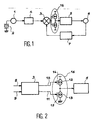
- Figure 1 shows the classical structure of a digital loop (PLL).
- a reference signal Fref generally derived from an oscillator 1 driven by a quartz 2, is applied to a phase comparator 3 via a frequency divider 4.
- the phase comparator 3 constitutes the heart of the PLL. It controls, via a loop filter 5, a voltage controlled oscillator VCO 6.
- the signal from the VCO 6 is applied, generally via a loop divider 7, to the comparator 3, which constitutes the loopback.
- the output of the device may be the signal from the VCO 6 or an intermediate signal of the loop divider 7.
- the frequency of the output signal can be changed.
- the frequency of the output signal is then slaved to the reference frequency Fref.
- the spectral purity and stability of the output signal are determined by the characteristics of the loop, and by the performance of the reference signal.
- Phase comparator circuit embodiments are given, for example, in the manual already cited for example on page 11 of this manual.
- the tri-state frequency phase comparator a state where the phase of the VCO is late on the reference phase, a state where the phase of the VCO is ahead of the reference phase and a so-called equilibrium state where these phases are in phases or in zones of delay or phase advance for which the phase loop can not react.
- the PFD tri-state phase comparator has the best capture performance and of linearity, making it the most used phase comparators in modern circuits.
- This PFD is done by adding a charge pump 16 whose role is to deliver a current function of the relative position of the inputs Fref and Fvco of the comparator.
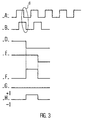
- FIG. 2 shows in more detail the phase comparator 3 and a charge pump circuit 16 immediately at the output of the tri-state comparator 3.
- the phase comparator 3 comprises a first 8 and a second 9 input respectively receiving the reference frequency Fref and a frequency from the VCO which is called F vco . It comprises two logic outputs 10, 11 respectively called up and down. These outputs 10, 11 respectively control current generators 12, 13 having control inputs 14, 15 respectively.
- the current generators 12, 13 together constitute the so-called charge pump 16 of the voltage controlled oscillator VCO 6.
- the generators 12, 13 deliver currents that are in principle equal, but in the opposite direction. Due to manufacturing tolerances, an imbalance generally exists between the absolute values of the currents delivered by the generators 12 and 13.
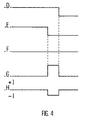
- the signals represented in line A and B of FIG. 3 represent the form of square periodic signals obtained in a known manner from the frequencies generated by reference oscillator 1 and VCO 6 respectively.
- the falling edge of the VCO signal is delayed with respect to the corresponding falling edge of the signal Fref as materialized in box C.
- the value present on the logic outputs 10 and 11 is represented on lines F and G respectively.
- the charging current of the pump 16 is represented on the line H. It can be a positive current of value + I, a negative current of value - I, or a zero current if none or the two generators of current 12 and 13 flow.
- a falling edge of the frequency Fref arriving before the falling edge of the frequency VCO will set the output 10 up (line F) to a logic value, for example 1, controlling a current output by the generator 12.
- the generator 12 will thus charge the pump for a period equal to the phase delay between Fvco and Fref. This charge has the effect of reducing the phase delay to O.
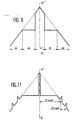
- FIG. 5 shows the case where the delay of the falling edge of the signal Fvco is little late or slightly in advance on the falling edge of the signal Fref and is for example in the shaded area shown in FIG. hatching of FIG. 5 corresponds to twice the minimum time necessary to put in flow the current generator 12 or 13.
- the charge pump 16 has not yet reacted to the order of debiting when it receives the order to no longer discharge.
- This curve represents the output power in ordinate with respect to the frequency in abscissa.
- This curve has two bearing zones substantially symmetrical to one another with respect to an axis YY 'corresponding to the value F vco .
- a marked frequency range C for which the axis YY 'is an axis of symmetry corresponds to a zone where, because of the reaction times Tpfd and Tcp, there is in fact no control over the output frequency Fvco.
- Frequency zones marked a and b in FIG. 6 correspond to the zones where, because of the phase control loop, the operation of the VCO will be enslaved in a stable manner, zones d and e placed in a substantially symmetrical manner, one by compared to the other, correspond again to frequency ranges where regulation is no longer exercised.
- the output power is regulated by the specific characteristics of the oscillator VC06.
- a known solution to remedy this defect is to reinject systematically a current pulse of predetermined duration triggered by the falling edge of Fref.
- the feedback is on the slowest channel triggered by Fref and the duration is set by design to ensure a current pulse regardless of the conditions of use of the phase loop.
- US-A-5699387 discloses a phase locked loop in which the charge re-injection time is set by a monostable multivibrator or a delay line.
- FIG. 1 A diagram showing an example circuit used for reinjection, is shown in FIG.
- the known feedback circuit intended to avoid the non-control zone c includes a charge feedback circuit 17 in the form of a generator 17 of a pulse of predetermined duration.
- An input 18 of this generator 17 receives Fref, and an output 19 carrying the output pulse, feeds a first input 23 of an OR gate 20.
- a second input 22 of this gate receives the output 10 (up) of the comparator 3.
- An output 21 of the OR gate 20 controls the current generator 12.
- the current generator 12 is controlled in flow rate for at least the duration ⁇ of the pulse supplied by the pulse generator 17.
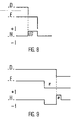
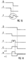
- FIGS. 8-10 show the same annotations as those in Figures 3-5.
- FIG. 8 represents the case where the phase delay of the signal Fvco is greater than the duration ⁇ , represented by a shaded area line H, of the pulse supplied by the pulse generator 17.
- the generator of current 12 will be controlled in flow rate by the two inputs of the OR gate 20.
- the flow rate of the generator 12 due to the pulse of the generator 17 is less than the flow time required to return to phase, the operation is identical to that described in connection with FIG. 3.
- the pulse of duration ⁇ does not change anything.
- the spectrum then has the appearance shown in FIG. 11. There is a power peak at the frequency Fvco, but moreover, repeated peaks at frequency intervals separated by the value of the frequency Fref.
- the inventor has noted that the spurious peaks are separated from each other by intervals equal to the value of the frequency Fref, and have an amplitude which is increasing with the duration of charge.
- the invention therefore consists in minimizing the charging time and therefore the amplitude of the variation of the charge, which is proportional to the duration ⁇ of the pulse generated by the generator 17. This reduces the amplitude of the peaks. parasites at the frequency Fref.
- the duration ⁇ of the pulse of the generator 17 according to the prior art shown in FIG. 7 must be greater than the reaction time T PFD of the phase comparator 3 plus the reaction time T CP of the current generator 12 or 13.
- the reaction time of the phase loop is, as explained above, the time that elapses between the arrival of a charge command and the moment when the charge current generator delivers with a current level. significant.
- a detector of the current delivered by the charge current generator said detector changing of logic level when the value of the current generated by the current generator becomes greater than a threshold value and we will use the change of this value. logic level to change the logic level at the output of the pulse generator.
- the invention relates to a phase-locked loop of a voltage-controlled oscillator, the loop comprising a phase comparator receiving as input a reference frequency and a frequency coming from the oscillator, and delivering values logic for controlling a pump charge, a charge feedback circuit receiving one of the inputs of the comparator and delivering a logic value for controlling the charge pump, loop characterized in that it further comprises a detector with a threshold value of one current representative of the current delivered by the charge pump, a logic output of the detector being applied back to the charge feedback circuit so as to limit the charge re-injection time.
- the current detector may be coupled to either the current generator actually included in the charge pump, or to an additional generator identical to the current generator included in the pump.
- the solution with additional generator has the disadvantage due to the manufacturing tolerances of having a trip threshold which can be slightly offset in time with respect to the tripping threshold of the generator included in the pump. To remedy this drawback, it will be possible to set the threshold of the current value triggering the change of logic level of the detector to a value slightly higher than that which one would have retained for the generator of the pump.
- the advantage of the additional generator is that the presence of the detector and the additional generator does not disturb the operation of the charge pump.
- the input of the charge feedback circuit is coupled not to the input of the comparator receiving the reference frequency, but to the input of the comparator receiving the frequency constructed from the output frequency of the oscillator.
- This embodiment has the advantage of further reducing the value of the average load current so that the height of the parasitic peaks separated from each other by the value of the frequency Fref. it is diminished.
- the invention also relates to a method as defined in claim 3, in which the reinjection duration is limited, not according to a predetermined reaction time of the phase loop but by limiting the duration of reinjection through detecting a current threshold value representative of the current supplied by the charge pump and applying, in return, a logic output of the detector to the charge feedback circuit.
- FIG. 12 represents a first example of a circuit including means for limiting the charge re-injection duration in accordance with the invention.
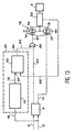
- the circuit according to the invention furthermore comprises a current detector receiving the charging current delivered by the charge pump 16. Moreover, a circuit 30 charge feedback 31 has an input 32 for limiting the duration of the charge feedback pulse.
- the charge regeneration circuit 31 comprises a generator 17 of a pulse of predetermined length ⁇ , as in the prior art. Instead of directly supplying the OR gate 20, the output 19 of the generator 17 feeds a first input 35 of a logic circuit 33. A second input of this logic circuit 33 is constituted by the input 32 carrying the logic value at the output of the detector 30. An output 34 of the logic circuit 33 constitutes the output of the charge feedback circuit 31. This output 34 is coupled to the first input 23 of the OR gate 20.
- the operation of the logic circuit 33 is as follows: when the first input 35 receives the logic value, for example 1, at the output 19 of the pulse generator 17, the output 34 of the circuit 33 takes a logic value, for example 1, controlling the flow of the current generator 12 of the pump 16. After a reaction time, the generator 12 will output. The flow rate of the generator 12 will be detected by the detector 30. As a result of this detection, the logic value at the output of the detector 30 will change to, for example, set to 1. As a result, the logic value at input 32 of the logic circuit 33 will also change.
- the circuit 33 is designed such that in this case the output 34 of this circuit steadily resumes the logic value, for example O, which controls a stop of the generator 12.
- the duration ⁇ of the pulse at the output of the feedback circuit 31, as modified by the invention is limited strictly to the time required to start up the current generator 12 and time to detect this startup.
- the operation of the circuit shown in FIG. 12 is identical to that of the circuit shown in FIG. 7 in conjunction with FIGS. 8 to 10, but because of the means for limiting the duration of the feedback pulse delivered by the feedback circuit 31, amplitude of variation of the charge level due to the charge pump 16 is limited.
- FIG. 13 A preferred embodiment of the loop portion around the phase comparator 3 is shown in FIG. 13. This embodiment is identical to that shown in FIG. 12 with the exception of the input of the pulse generator 17. According to this mode embodiment, the input 18 of the pulse generator 17 receives not the signal Fref but the signal F vco .
- the signal Fref line D is late on the signal F vco line E.
- the input 18 of the pulse generator 31 receives a logic signal which triggers an output having a logic value triggering the current of the current generator 12 for a duration ⁇ corresponding to the duration of the pulse of the feedback circuit 31.
- the current represented line H delivered by the current pump 16 is the algebraic sum of the opposite currents delivered by the generators 12 and 13.
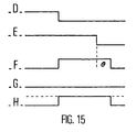
- FIG. 15 shows the operation of the device represented in FIG. 13 when the signal F vco (line E) is out of phase with respect to the signal Fref (line D).
- the arrival of the falling edge of Fref triggers the transition to 1 of the output 10 (up) of the comparator 3 (line F).
- the control of the generator 12 is positive and the rest (line F) until the arrival of the falling edge of the signal F vco .
- the output 10 returns to 0, which is represented by a dotted line F.
- the arrival of the falling edge of the signal F vco triggers for a duration ⁇ the pulse of the generator 31.
- the other input 23 of the OR gate 20 becomes positive when the input 22 returns to 0. Under these conditions, the output 21 of the OR gate 20 remains at 1 and the generator (up) 12 continues to debit. .
- the value of the current delivered by the pump 16, represented as line H, is equal to + I for a duration equal to the time separating the falling edges of the signals Fref and F vco plus the duration ⁇ of the pulse delivered. by the pulse generator 31.
- the level of the first stray line is 18 dB below the reinjection circuits according to the prior art.
- FIG. 17 An embodiment of the invention with an auxiliary current generator for detection is shown in FIG. 17.
- This variant embodiment is shown in FIG. 17 as a variant of the circuit represented in FIG. 13. It is applicable exactly under the same conditions to the circuit represented in FIG. 12.
- the circuit comprises an additional charge pump 40.
- This additional charge pump receives the output of the OR gate 21 and the output 11 of the comparator 3.
- the detector 30 receives the output current of the additional pump 40.
- the invention is also applicable to oscillators with a negative control slope.
Landscapes
- Stabilization Of Oscillater, Synchronisation, Frequency Synthesizers (AREA)
Claims (3)
- Phasenverriegelungsschleife eines spannungsgesteuerten Oszillators (6), wobei die Schleife einen Phasenkomparator (3), der als Eingang (8, 9) eine Referenzfrequenz und eine von dem Oszillator (6) stammende Frequenz erhält und logische Werte zur Steuerung einer Ladepumpe (16) liefert, und einen Ladungswiedereinspeisungs-Schaltkreis (31) umfasst, der einen der Eingänge (8, 9) des Komparators (3) erhält und einen logischen Wert zur Steuerung der Ladepumpe (16) liefert,
dadurch gekennzeichnet, dass sie außerdem einen Detektor (30) eines Schwellenwerts eines für den durch die Ladepumpe (16) gelieferten Strom repräsentativen Stroms umfasst und ein logischer Ausgang des Detektors (30) auf den Ladungswiedereinspeisungs-Schaltkreis (31) rückgekoppelt ist, um die Dauer der Ladungswiedereinspeisung zu begrenzen. - Schleife nach Anspruch 1, dadurch gekennzeichnet, dass der Ladungswiedereinspeisungs-Schaltkreis umfasst:- einen Impulsgenerator (17) mit einem Eingang (18), wobei dieser Eingang (18) der Eingang (18) des Wiedereinspeisungs-Schaltkreises (31) ist, und einem Ausgang (19);- einen Logikschaltkreis (33) mit zwei Eingängen (19, 32) und einem Ausgang (34), wobei einer der Eingänge (19) des genannten Logikschaltkreises (33) gekoppelt ist mit dem Ausgang (19) des Impulsgenerators (17), und der andere Eingang (32) gekoppelt ist mit dem Ausgang (34) des genannten Logikschaltkreises (33), der den Ausgang (34) des Wiedereinspeisungs-Schaltkreises (31) bildet.
- Verfahren zur Reduzierung eines Pegels von Störlinien, geliefert durch einen Oszillator (6), der spannungsgesteuert ist und kontrolliert wird durch eine Phasenschleife, die einen Phasenkomparator, der als Eingang (8, 9) eine Referenzfrequenz und eine von dem Oszillator (6) stammende Frequenz erhält und logische Werte zur Steuerung einer Ladepumpe (16) liefert, und einen Ladungswiedereinspeisungs-Schaltkreis (31) umfasst, der einen der Eingänge (8, 9) des Komparators (3) erhält und einen logischen Wert zur Steuerung der Ladepumpe (16) liefert, wobei dieses Verfahren dadurch gekennzeichnet ist, dass man die Dauer der Wiedereinspeisung begrenzt, indem man in einem Detektor (30) einen Schwellenwert eines für den durch die Ladepumpe (16) gelieferten Strom repräsentativen Stroms detektiert und indem man einen logischen Ausgang des Detektors auf den Ladungswiedereinspeisungs-Schaltkreis (31) rückkoppelt.
Applications Claiming Priority (2)
| Application Number | Priority Date | Filing Date | Title |
|---|---|---|---|
| FR9914055 | 1999-11-09 | ||
| FR9914055A FR2800939B1 (fr) | 1999-11-09 | 1999-11-09 | Boucle numerique a verrouillage de phase |
Publications (2)
| Publication Number | Publication Date |
|---|---|
| EP1100201A1 EP1100201A1 (de) | 2001-05-16 |
| EP1100201B1 true EP1100201B1 (de) | 2007-04-11 |
Family
ID=9551898
Family Applications (1)
| Application Number | Title | Priority Date | Filing Date |
|---|---|---|---|
| EP00403067A Expired - Lifetime EP1100201B1 (de) | 1999-11-09 | 2000-11-06 | Digitaler Phasenregelkreis |
Country Status (4)
| Country | Link |
|---|---|
| US (1) | US6388531B1 (de) |
| EP (1) | EP1100201B1 (de) |
| DE (1) | DE60034292D1 (de) |
| FR (1) | FR2800939B1 (de) |
Families Citing this family (4)
| Publication number | Priority date | Publication date | Assignee | Title |
|---|---|---|---|---|
| US6717475B2 (en) * | 2001-11-01 | 2004-04-06 | Skyworks Solutions, Inc. | Fast-acquisition phase-locked loop |
| CN1671050B (zh) * | 2004-09-30 | 2010-04-14 | 东南大学 | 压控振荡器用稳幅电路 |
| US8648634B2 (en) * | 2012-05-10 | 2014-02-11 | International Business Machines Corporation | Input jitter filter for a phase-locked loop (PLL) |
| CN104617950A (zh) * | 2015-01-31 | 2015-05-13 | 复旦大学 | 一种集成的调频连续波数字频率综合器 |
Family Cites Families (7)
| Publication number | Priority date | Publication date | Assignee | Title |
|---|---|---|---|---|
| US4814726A (en) * | 1987-08-17 | 1989-03-21 | National Semiconductor Corporation | Digital phase comparator/charge pump with zero deadband and minimum offset |
| US5036216A (en) * | 1990-03-08 | 1991-07-30 | Integrated Circuit Systems, Inc. | Video dot clock generator |
| US5699387A (en) * | 1993-06-23 | 1997-12-16 | Ati Technologies Inc. | Phase offset cancellation technique for reducing low frequency jitters |
| FR2717019A1 (fr) * | 1994-03-02 | 1995-09-08 | Philips Composants | Dispositif oscillateur verrouillé en phase. |
| JP3395818B2 (ja) * | 1996-04-19 | 2003-04-14 | ソニー株式会社 | Pll回路とそれを用いた信号処理装置 |
| US5949264A (en) * | 1996-11-29 | 1999-09-07 | Lo; Dennis C. | Digital phase detector and charge pump system reset and balanced current source matching methods and systems |
| US6278333B1 (en) * | 2000-02-29 | 2001-08-21 | Motorola, Inc. | Phase lock loop with dual state charge pump and method of operating the same |
-
1999
- 1999-11-09 FR FR9914055A patent/FR2800939B1/fr not_active Expired - Fee Related
-
2000
- 2000-11-06 EP EP00403067A patent/EP1100201B1/de not_active Expired - Lifetime
- 2000-11-06 DE DE60034292T patent/DE60034292D1/de not_active Expired - Lifetime
- 2000-11-07 US US09/707,376 patent/US6388531B1/en not_active Expired - Lifetime
Also Published As
| Publication number | Publication date |
|---|---|
| FR2800939B1 (fr) | 2002-01-25 |
| EP1100201A1 (de) | 2001-05-16 |
| DE60034292D1 (de) | 2007-05-24 |
| FR2800939A1 (fr) | 2001-05-11 |
| US6388531B1 (en) | 2002-05-14 |
Similar Documents
| Publication | Publication Date | Title |
|---|---|---|
| FR2882871A1 (fr) | Oscillateur commande en tension a multiphase realignee et boucle a phase asservie associee | |
| FR2706229A1 (fr) | Procédé d'amélioration de l'immunité au bruit d'une boucle à verrouillage de phase et dispositif mettant en Óoeuvre ce procédé. | |
| FR2738425A1 (fr) | Methode et appareil pour controler une plage d'accord d'un oscillateur commande en tension dans un synthetiseur de frequences | |
| FR2787651A1 (fr) | Detecteur numerique de frequence de phase | |
| EP0142440A2 (de) | Vorrichtung zum Erzeugen einer, bezüglich einer Referenzfrequenz gebrochenen Frequenz | |
| FR2473816A1 (fr) | Systeme a blocage de boucle | |
| EP0670629B1 (de) | Phasenregelkreis | |
| EP0564377A1 (de) | Frequenzregelschleife | |
| FR2465370A1 (fr) | Circuit de compensation de surmodulation de sous-modulation et de retard transitoires dans des systemes comportant des reseaux de filtres reactifs | |
| EP0881772B1 (de) | Frequenzteilungsvorrichtung, bestehend aus einem Vorzähler gefolgt von einem programmierbaren Zähler und Anwendung in einem Frequenzsynthetisierer | |
| FR2840469A1 (fr) | Boucle a verrouillage de phase | |
| FR2800939A1 (fr) | Boucle numerique a verrouillage de phase | |
| EP0434527B1 (de) | Mikrowellen-Synthesierer mit einem Teiler mit gebrochenem Teilverhältnis | |
| BE897822A (fr) | Circuit de pretection pour ballast capacitif | |
| EP1133060B1 (de) | Phasenregelschleife zur Erzeugung eines Referenzsignals hoher spektraler Reinheit | |
| EP0218508B1 (de) | Schnell variierbarer Frequenzgenerator | |
| EP1710916B1 (de) | Phasenregelschleife | |
| EP0835550B1 (de) | Phasenkomparator ohne totbereich | |
| FR2816075A1 (fr) | Generateur ameliore pour la production de signaux d'horloge | |
| FR2479590A1 (fr) | Circuit de protection a reponse rapide pour transistor de puissance, et dispositif d'alimentation electrique a decoupage comportant un tel circuit | |
| EP1411638B1 (de) | Verfahren und Vorrichtung zur Erzeugung eines Signals mit einer dem Produkt einer Referenzfrequenz mit einer reellen Zahl entsprechenden Frequenz | |
| FR2864377A1 (fr) | Boucle a asservissement de phase | |
| EP1211811A1 (de) | Schnelle Frequenzvergleichsschaltung | |
| FR2624673A1 (fr) | Oscillateur a commande numerique, utilisant un element commutable, application a la realisation de dispositifs de recuperation du rythme et de la phase d'un signal numerique | |
| FR2600848A1 (fr) | Dispositif d'asservissement d'un oscillateur a une source hyperfrequence a tres faible bruit de phase et agile en frequence |
Legal Events
| Date | Code | Title | Description |
|---|---|---|---|
| PUAI | Public reference made under article 153(3) epc to a published international application that has entered the european phase |
Free format text: ORIGINAL CODE: 0009012 |
|
| AK | Designated contracting states |
Kind code of ref document: A1 Designated state(s): DE FR GB IT |
|
| AX | Request for extension of the european patent |
Free format text: AL;LT;LV;MK;RO;SI |
|
| 17P | Request for examination filed |
Effective date: 20010906 |
|
| RAP1 | Party data changed (applicant data changed or rights of an application transferred) |
Owner name: STMICROELECTRONICS S.A. |
|
| AKX | Designation fees paid |
Free format text: DE FR GB IT |
|
| GRAP | Despatch of communication of intention to grant a patent |
Free format text: ORIGINAL CODE: EPIDOSNIGR1 |
|
| GRAS | Grant fee paid |
Free format text: ORIGINAL CODE: EPIDOSNIGR3 |
|
| GRAA | (expected) grant |
Free format text: ORIGINAL CODE: 0009210 |
|
| AK | Designated contracting states |
Kind code of ref document: B1 Designated state(s): DE FR GB IT |
|
| REG | Reference to a national code |
Ref country code: GB Ref legal event code: FG4D Free format text: NOT ENGLISH |
|
| REF | Corresponds to: |
Ref document number: 60034292 Country of ref document: DE Date of ref document: 20070524 Kind code of ref document: P |
|
| GBT | Gb: translation of ep patent filed (gb section 77(6)(a)/1977) |
Effective date: 20070627 |
|
| PLBE | No opposition filed within time limit |
Free format text: ORIGINAL CODE: 0009261 |
|
| STAA | Information on the status of an ep patent application or granted ep patent |
Free format text: STATUS: NO OPPOSITION FILED WITHIN TIME LIMIT |
|
| 26N | No opposition filed |
Effective date: 20080114 |
|
| PG25 | Lapsed in a contracting state [announced via postgrant information from national office to epo] |
Ref country code: DE Free format text: LAPSE BECAUSE OF FAILURE TO SUBMIT A TRANSLATION OF THE DESCRIPTION OR TO PAY THE FEE WITHIN THE PRESCRIBED TIME-LIMIT Effective date: 20070712 Ref country code: IT Free format text: LAPSE BECAUSE OF FAILURE TO SUBMIT A TRANSLATION OF THE DESCRIPTION OR TO PAY THE FEE WITHIN THE PRESCRIBED TIME-LIMIT Effective date: 20070411 |
|
| GBPC | Gb: european patent ceased through non-payment of renewal fee |
Effective date: 20071106 |
|
| REG | Reference to a national code |
Ref country code: FR Ref legal event code: ST Effective date: 20080930 |
|
| PG25 | Lapsed in a contracting state [announced via postgrant information from national office to epo] |
Ref country code: GB Free format text: LAPSE BECAUSE OF NON-PAYMENT OF DUE FEES Effective date: 20071106 |
|
| PG25 | Lapsed in a contracting state [announced via postgrant information from national office to epo] |
Ref country code: FR Free format text: LAPSE BECAUSE OF NON-PAYMENT OF DUE FEES Effective date: 20071130 |