EP1096565B1 - Sealed-by-resin type semiconductor device and liquid crystal display module including the same - Google Patents
Sealed-by-resin type semiconductor device and liquid crystal display module including the same Download PDFInfo
- Publication number
- EP1096565B1 EP1096565B1 EP00123049A EP00123049A EP1096565B1 EP 1096565 B1 EP1096565 B1 EP 1096565B1 EP 00123049 A EP00123049 A EP 00123049A EP 00123049 A EP00123049 A EP 00123049A EP 1096565 B1 EP1096565 B1 EP 1096565B1
- Authority
- EP
- European Patent Office
- Prior art keywords
- resin
- sealed
- semiconductor device
- type semiconductor
- substrate
- Prior art date
- Legal status (The legal status is an assumption and is not a legal conclusion. Google has not performed a legal analysis and makes no representation as to the accuracy of the status listed.)
- Expired - Lifetime
Links
Images

Classifications
-
- H—ELECTRICITY
- H10—SEMICONDUCTOR DEVICES; ELECTRIC SOLID-STATE DEVICES NOT OTHERWISE PROVIDED FOR
- H10W—GENERIC PACKAGES, INTERCONNECTIONS, CONNECTORS OR OTHER CONSTRUCTIONAL DETAILS OF DEVICES COVERED BY CLASS H10
- H10W76/00—Containers; Fillings or auxiliary members therefor; Seals
- H10W76/10—Containers or parts thereof
-
- H—ELECTRICITY
- H10—SEMICONDUCTOR DEVICES; ELECTRIC SOLID-STATE DEVICES NOT OTHERWISE PROVIDED FOR
- H10W—GENERIC PACKAGES, INTERCONNECTIONS, CONNECTORS OR OTHER CONSTRUCTIONAL DETAILS OF DEVICES COVERED BY CLASS H10
- H10W74/00—Encapsulations, e.g. protective coatings
- H10W74/01—Manufacture or treatment
- H10W74/012—Manufacture or treatment of encapsulations on active surfaces of flip-chip devices, e.g. forming underfills
-
- H—ELECTRICITY
- H10—SEMICONDUCTOR DEVICES; ELECTRIC SOLID-STATE DEVICES NOT OTHERWISE PROVIDED FOR
- H10W—GENERIC PACKAGES, INTERCONNECTIONS, CONNECTORS OR OTHER CONSTRUCTIONAL DETAILS OF DEVICES COVERED BY CLASS H10
- H10W74/00—Encapsulations, e.g. protective coatings
- H10W74/10—Encapsulations, e.g. protective coatings characterised by their shape or disposition
- H10W74/15—Encapsulations, e.g. protective coatings characterised by their shape or disposition on active surfaces of flip-chip devices, e.g. underfills
-
- H—ELECTRICITY
- H10—SEMICONDUCTOR DEVICES; ELECTRIC SOLID-STATE DEVICES NOT OTHERWISE PROVIDED FOR
- H10W—GENERIC PACKAGES, INTERCONNECTIONS, CONNECTORS OR OTHER CONSTRUCTIONAL DETAILS OF DEVICES COVERED BY CLASS H10
- H10W72/00—Interconnections or connectors in packages
- H10W72/851—Dispositions of multiple connectors or interconnections
- H10W72/853—On the same surface
- H10W72/856—Bump connectors and die-attach connectors
Definitions
- the present invention relates to a sealed-by-resin type semiconductor device and a liquid crystal display module including the same. More particularly, the present invention relates to a COF (chip on flexible printed circuit) in which ICs and chips are implemented on a flexible substrate, and a liquid crystal display module including the same.
- COF chip on flexible printed circuit
- LCD liquid crystal display
- an IC for driving a liquid crystal hereinafter referred to as an LC-driving IC
- LC-driving IC an IC for driving a liquid crystal
- other chips are mounted on a flexible substrate made of a polyimide film printed with a conductor pattern, and these elements are coupled to an LCD element via an anisotropic conductive film.
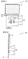
- Figure 5 is a plan view of such a COF LCD module.
- Figure 6 is a side view of the COF LCD module.
- a “sealing resin” herein means a resin which fills between an LC-driving IC and a flexible substrate so as to protect a contact between the LC-driving IC and the flexible substrate.
- a COF LCD module 400 includes an LCD element 8 and a COF 300 .
- the COF 300 includes a flexible substrate 9 on which an LC-driving IC 1 and a chip 10 are mounted.
- the flexible substrate 9 is, for example, fabricated in the following way.
- a copper foil having a thickness of about 2 to 35 ⁇ m is coated with a precursor of polyimide which is in turn cured.
- the resultant polyimide film substrate has a thickness of about 10 to 100 ⁇ m.
- Such a fabricating method is called casting.
- the substrate is etched to obtain the desired conductor pattern.
- the substrate is coated with a polyimide resin or an epoxy resin, except for portions of the substrate 9 on which the LC-driving IC 1 and the chip 10 and contacts of the LCD element 8 with the LC-driving IC 1 and the chip 10 .
- the conductor pattern on which a conductor is exposed is plated with Sn, Ni, Au, or the like. In this way, the flexible substrate 9 is fabricated.
- an additive method may be employed.
- a sputtered copper is patterned and then thickened by plating.
- the COF 300 is, for example, fabricated in the following way.
- the LC-driving IC 1 and the chip 10 are mounted on the conductor pattern of the flexible substrate 9 .
- the LC-driving IC 1 is implemented by flip chip bonding.
- the LC-driving IC 1 includes an Au bump (not shown) which is coupled with the conductor pattern.
- an Au bump (not shown) which is coupled with the conductor pattern.
- an Sn-Au alloy coupling method, or a coupling method using an anisotropic conductive film may be adopted.
- the Sn-Au alloy coupling method is performed in the following way.
- the LC-driving IC 1 is provided on the flexible substrate 9 so that the Au bump of the LC-driving IC 1 contacts with the Sn-plated conductor pattern.
- the Au bump is coupled with the conductor pattern by heating and pressing the flexible substrate 9 from the rear side thereof ( 9A side). Subsequently, the LC-driving IC 1 is sealed by a sealing resin 4 .
- the coupling method using an anisotropic conductive film is performed in the following way.
- the anisotropic conductive film is interposed between the flexible substrate 9 and the LC-driving IC 1 .
- the flexible substrate 9 is heated and pressed from the rear side thereof ( 9A side) so that the Au bump is electrically coupled with the conductor pattern while the Au bump is fixed on the conductor pattern by the cured anisotropic conductive film.
- the COF 300 fabricated as described above is conductive-coupled with the LCD element 8 using an anisotropic conductive film or the like, thereby obtaining the LCD module 400 .
- the Au bump is used as the segment output terminal of the LC-driving IC 1 .
- the coupling strength between the LC-driving IC 1 and the flexible substrate 9 needs to be enhanced and the COF 300 on which the LC-driving IC 1 is mounted needs to be thinner.
- the inventors fabricated and studied a prototype of the COF 300 , in which the LC-driving IC 1 having an Au bump having a narrower pitch, is mounted on the flexible substrate 9 by the Sn-Au alloy coupling.
- the Au migration is generated by an electric field being applied to a halogen and moisture.
- the document WO 98 20542 A corresponding to EP 0 957 513 , describes an electronic component part device having a packaging substrate and at least one electronic component part mounted on the packaging substrate wherein a bump electrode and the packaging substrate are connected through an adhesive film.
- the adhesive film is used to reduce heat stress at the time of heat cycling and to reduce undulation of electrode surfaces to increase the connection reliability.
- the adhesive film may contain thermosetting resin, epoxy resin or imide resin.
- the adhesive has a storage elastic modulus at 40°C after bonding, of from 100 to 4,000 MPa, while the in the preferred embodiments the elastic modulus is 1,200 MPa and 1,500 MPa, respectively.
- the document US-A-5 959 363 relates to a semiconductor device with a semiconductor chip being mounted on a circuit board through a bump electrode, and it discloses the use of two different encapsulation resins, one first resin disposed within an inner surrounded by the electrode connections and one second resin disposed in an outer region disposed beyond the leads positioned on the outermost periphery of the semiconductor device.
- the purpose of the use of the two different resins is to alleviate stress distortion.
- the resin may contain epoxy resin such as a bisphenol type epoxy resin or polyimide resin.
- the two different encapsulation resins contain a filler, the fillers having different particle diameters and different particle contents in each of the two resins.
- the preferred elastic modulus of the first resin is selected to be 900x10 7 Pa and the preferred elastic modulus of the second resin is selected to be 1200x10 7 Pa.
- the document US-A-5 916 688 discloses resin solutions having improved curing temperatures and improved solvent solubility.
- the resin may contain polyimide resin composed of aromatic tetra carboxylic acids and aromatic diamines.
- the resin solutions have a low elastic modulus.
- EP-A-0 422 906 discloses an LCD device comprising electrodes mounted on a substrate and is concerned with a connection resistance of semiconductor devices mounted on substrates.
- EP-A-0 303 256 discloses an electrode and a substrate connected through an electroconductive adhesive resin.
- the adhesive resin is suitable for easy removal from a glass substrate.
- a sealed-by-resin type semiconductor device includes: a substrate; a lead provided on the substrate; and a semiconductor element provided on the lead by flip chip bonding; wherein the semiconductor element includes a plurality of terminals connected to the lead, and wherein the plurality of terminals include an Au bump; the sealed-by-resin type semiconductor device further includes a resin for protecting the plurality of terminals; and the device being characterized in that the resin has a sufficiently low elasticity modulus that occurrence of undesirable migration is suppressed and the resin has a sufficiently high elasticity modulus that a coupling strength between the substrate and the semiconductor is sufficient, wherein the elasticity modulus is at least 0.3 GPa and at most 1 GPa.
- the resin includes a thermosetting resin, an epoxy resin, or a denatured polyimide resin.
- the resin includes an epoxy resin and the epoxy resin includes a bisphenol resin.
- the resin includes a denatured polyimide resin and the denatured polyimide resin includes aromatic tetracarboxylic acid and aromatic diamine.
- a pitch of the plurality of terminals is at most 70 ⁇ m.
- a liquid crystal display element is coupled with the substrate to form a liquid crystal display module.
- the liquid crystal display module further includes an anisotropic conductive film for coupling the substrate with the liquid crystal display element.
- the inventors conducted an experiment in which an Au bump to which a halogen compound was attached was exposed to high temperature and high humidity. As a result, occurrence of migration was suppressed and a sufficient coupling strength was obtained between the LC-driving IC 1 and the flexible substrate 9 when the elasticity modulus of the sealing resin 4 sealing the LC-driving IC 1 was optimized. This led to achievement of the present invention.
- the electrical coupling reliability of the semiconductor elements and the flexible circuit substrate such as heat-impact resistance, moisture resistance, and a coupling strength can be enhanced.
- An epoxy resin or a denatured polyimide resin is used as the sealing resin.
- the invention described herein makes possible the advantages of (1) providing a sealed-by-resin type semiconductor device capable of suppressing migration between Au bumps, and an LCD module including the same and (2) providing a sealed-by-resin type semiconductor device having a sufficient coupling strength between an LC-driving IC and a flexible substrate.
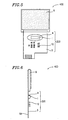
- Figure 1 is a plan view of a COF LCD module 200 according to an embodiment of the present invention.
- Figure 2 is a side view of a COF LCD module 200 according to the embodiment of the present invention.
- the same components as those included in the COF LCD module 400 are indicated by the same reference numerals as those used for the COF LCD module 400 . Detailed description is omitted for those components.
- the COF LCD module 200 includes an LCD element 8 and a COF 100 .
- the COF 100 includes a flexible substrate 9 on which an LC-driving IC 1 and a chip 10 are mounted.
- the COF LCD module 200 according to the embodiment of the present invention is different from the foregoing COF LCD module 400 in that in the COF LCD module 200 the LC-driving IC 1 is sealed by a sealing resin 12 , of which the elasticity modulus is optimized, instead of the sealing resin 4 .
- Figure 3 is a cross-sectional view of a major portion of the COF 100 according to the embodiment of the present invention.
- the sealing resin 12 seals the LC-driving IC 1 .
- a given electronic circuit (not shown) and an electrode pad 1B are provided on a rear side 1A of the LC-driving IC 1 .
- the Au bump 3 is provided on the electrode pad 1B .
- the outer dimensions of the LC-driving IC 1 are about 2 mm ⁇ 20 mm.
- the bump height H is about 15 ⁇ m.
- the minimum bump pitch P of the Au bump 3 is about 80 ⁇ m.
- the flexible substrate 9 includes a polyimide film 2 having a thickness of about 20 to 30 ⁇ m, a conductor pattern 5 of Cu provided on the polyimide film 2 , a portion on which the LC-driving IC 1 is mounted, a portion on which the chip 10 is mounted, an ink coverlay 6 of polyimide covering portions other than a connecting terminal 9A which connects an LCD element 8 and the COF 100 , an Sn plating layer 7 with which the conductor pattern 5 is coated.
- the flexible substrate 9 and the LC-driving IC 1 are registered so that the conductor pattern 5 is opposed to the Au bump 3 .
- the LC-driving IC 1 is heated and pressed from the top side thereof (in the direction indicated by arrow A) so as to couple the conductor patterns with the Au bump 3 due to an Sn-Au alloyed junction.
- the heating temperature is about 280°C or more which is sufficient so that the Sn plating layer 7 and the Au bump 3 form into an eutectic alloy.
- a sealing resin 12 is injected into a gap between the LC-driving IC 1 and the flexible substrate 9 .
- the sealing resin 12 is cured to seal the gap.
- the sealing resin 12 has an elasticity modulus which is sufficiently low so as not to generate undesirable migration.
- a resin is applied to the LC-driving IC 1 using a dispenser.
- the resin is heated for about two hours at about 100°C and then for about one hour at about 150°C so as to be cured.
- a transparent electrode connecting terminal 8A of the LCD element 8 is electrically coupled with a connecting terminal 9A of the flexible substrate 9 via an anisotropic conductive film.
- the LCD module 200 is completely fabricated.
- Example 1 a bisphenol type epoxy resin was used as the sealing resin.
- the elasticity modulus was measured by a dynamic viscoelasticity method (conducted at a room temperature of about 25°C).
- LCD modules were fabricated for each of the four types of bisphenol type epoxy resins having elasticity modulus of 0.005 GPa, 0.07 GPa, 0.3 GPa, and 1.0 GPa, respectively. All the LCD modules were placed in a moisture-resistance reliability test bath having a temerature of about 60°C and a humidity of about 95%. The rate of occurrence of an LCD abnormality, which is caused by leakage between the Au bumps due to the migration, was evaluated after about 1000 hours had passed.
- Figure 4 is a graph showing the rate of occurrence of the LCD abnormality that is caused by leakage between the Au bumps due to the migration, in Example 1. As is seen from Figure 4 , when the bisphenol type epoxy resin was used as the sealing resin 12 in Example 1, there were substantially no LCD abnormality that is caused by leakage between the Au bumps due to the migration.
- the coupling strength between the LC-driving IC 1 and the flexible substrate 9 was evaluated.
- the flexible substrate 9 was bent into a 90° angle while the LC-driving IC 1 was fixed on the flexible substrate 9 .
- a load was increasingly imposed on the LC-driving IC 1 while the LCD element 8 was displaying. In this case, the value of the load, which starts to generate the display abnormality in the LCD element 8 , was determined.
- the inventors' previous study has found that when the value of the load, which starts to generate the display abnormality in the LCD element 8 , is about 500 gf or more, there are substantially no adverse problems in the process of incorporating the COF LCD module into a device.
- Table 1 shows the values of loads which start to generate the display abnormality in the LCD elements having the respective elasticity.
- Table 1 Example 1 ( epoxy)
- Example 2 polyimide)
- Conventional example 1 epoxy
- Conventional example 2 Silicone
- Average value gf) 380 730 1220 1380 950 970 1510 1500 210
- Minimum value (gf) 350 690 1080 1100 880 860 1330 1350 180
- the values of loads are 500 gf or more.
- the epoxy resins used in Example 1 have shorter cure time, thereby improving productivity.
- Example 2 a denatured polyimide including aromatic tetracarboxylic acid and aromatic diamine was used as the sealing resin. Two types of the denatured polyimide having elasticity modulus of 0.45 GPa and 0.65 GPa, respectively. The elasticity modulus was measured by the dynamic viscoelasticity method, similar to Example 1 (conducted at a room temperature of about 25°C).
- COF LCD modules 200 were fabricated for each of the two types of the denatured polyimide having elasticity modulus of 0.45 GPa and 0.65 GPa, respectively, in a way similar to Example 1.
- the sealing resin was heated for two hours at 90°C and then for two hours at 150°C.
- the coupling strength between the LC-driving IC 1 and the flexible substrate 9 was evaluated in a way similar to that of Example 1 and the results are shown in Table 1.
- the obtained values of loads are 500 gf or more.
- the denatured polyimide having elasticity modulus of 0.07 GPa or more and 1 GPa or less has the same effect as that of Example 1.
- Example 1 In Conventional Example 1, two types of epoxy resins having elasticity modulus of 2.5 GPa and 3.1 Gpa, which are higher than the elasticity modulus of the sealing resins of Examples 1 and 2, were used.
- Example 2 Similar to Example 1, 50 COF LCD modules were fabricated for each elasticity modulus. The sealing resins were cured for two hours at 120°C and then for two hours at 150°C. All the COF LCD modules were subjected to a moisture-resistance reliability test similar to that of Example 1.
- Example 2 a silicone resin having an elasticity modulus of 0.0006 GPa, which is lower than the elasticity modulus of the sealing resins of Examples 1 and 2, was used.
- Example 2 Similar to Example 1, 50 COF LCD modules were fabricated. The sealing resin was cured for four hours at 150°C. The COF LCD modules were subjected to a moisture-resistance reliability test similar to that of Example 1.
- the present invention can provide the sealed-by-resin type semiconductor device capable of suppressing occurrence of migration between the Au bumps, and an LCD module including the same.
- the present invention can provide the sealed-by-resin type semiconductor device having a sufficient coupling strength between the LC-driving IC and the flexible substrate, and an LCD module including the same.
- the epoxy resin or denatured polyimide resin having an elasticity modulus of 0.07 GPa or more and 1 GPa or less is used as a sealing resin protecting semiconductor elements. Therefore, it is possible to suppress occurrence of migration which is responsible for the leakage between the Au bumps. Moreover, a coupling strength between the semiconductor elements and the flexible substrate is sufficient, which is an excellent, characteristic effect.
Landscapes
- Wire Bonding (AREA)
- Structures Or Materials For Encapsulating Or Coating Semiconductor Devices Or Solid State Devices (AREA)
- Liquid Crystal (AREA)
- Devices For Indicating Variable Information By Combining Individual Elements (AREA)
- Structures For Mounting Electric Components On Printed Circuit Boards (AREA)
- Encapsulation Of And Coatings For Semiconductor Or Solid State Devices (AREA)
Description
- The present invention relates to a sealed-by-resin type semiconductor device and a liquid crystal display module including the same. More particularly, the present invention relates to a COF (chip on flexible printed circuit) in which ICs and chips are implemented on a flexible substrate, and a liquid crystal display module including the same.
- Recently, there is a demand for smaller-sized, lighter, thinner elements for use in electronic devices such as personal digital assistants. One of such elements is a liquid crystal display (hereinafter referred to as LCD) module which is used as an output section of the electronic devices. Ease of incorporation into the devices is highly required.
- Some LCD modules are created by the COF technique to meet the above-described demand. In such an LCD module, an IC for driving a liquid crystal (hereinafter referred to as an LC-driving IC) and other chips are mounted on a flexible substrate made of a polyimide film printed with a conductor pattern, and these elements are coupled to an LCD element via an anisotropic conductive film.
- Figure 5 is a plan view of such a COF LCD module.
Figure 6 is a side view of the COF LCD module. - A "sealing resin" herein means a resin which fills between an LC-driving IC and a flexible substrate so as to protect a contact between the LC-driving IC and the flexible substrate.
- As shown in Figure 5, a
COF LCD module 400 includes anLCD element 8 and aCOF 300. The COF 300 includes aflexible substrate 9 on which an LC-drivingIC 1 and achip 10 are mounted. - The
flexible substrate 9 is, for example, fabricated in the following way. A copper foil having a thickness of about 2 to 35 µm is coated with a precursor of polyimide which is in turn cured. The resultant polyimide film substrate has a thickness of about 10 to 100 µm. Such a fabricating method is called casting. The substrate is etched to obtain the desired conductor pattern. The substrate is coated with a polyimide resin or an epoxy resin, except for portions of thesubstrate 9 on which the LC-drivingIC 1 and thechip 10 and contacts of theLCD element 8 with the LC-drivingIC 1 and thechip 10. The conductor pattern on which a conductor is exposed is plated with Sn, Ni, Au, or the like. In this way, theflexible substrate 9 is fabricated. - As an alternative way to form the conductor pattern, an additive method may be employed. In this case, a sputtered copper is patterned and then thickened by plating.
- The COF 300 is, for example, fabricated in the following way. The LC-driving
IC 1 and thechip 10 are mounted on the conductor pattern of theflexible substrate 9. The LC-driving IC 1 is implemented by flip chip bonding. - The LC-driving
IC 1 includes an Au bump (not shown) which is coupled with the conductor pattern. As a method of coupling the Au bump with the conductor pattern, for example, an Sn-Au alloy coupling method, or a coupling method using an anisotropic conductive film may be adopted. - The Sn-Au alloy coupling method is performed in the following way. The LC-driving IC 1 is provided on the
flexible substrate 9 so that the Au bump of the LC-drivingIC 1 contacts with the Sn-plated conductor pattern. The Au bump is coupled with the conductor pattern by heating and pressing theflexible substrate 9 from the rear side thereof (9A side). Subsequently, the LC-drivingIC 1 is sealed by a sealingresin 4. - The coupling method using an anisotropic conductive film is performed in the following way. The anisotropic conductive film is interposed between the
flexible substrate 9 and the LC-drivingIC 1. In this situation, theflexible substrate 9 is heated and pressed from the rear side thereof (9A side) so that the Au bump is electrically coupled with the conductor pattern while the Au bump is fixed on the conductor pattern by the cured anisotropic conductive film. - Thereafter, the COF 300 fabricated as described above is conductive-coupled with the
LCD element 8 using an anisotropic conductive film or the like, thereby obtaining theLCD module 400. - Recently, the pitch of the Au bump is becoming narrower in order to meet a demand for a higher resolution of liquid crystal display and a smaller area of the LC-driving
IC 1. The Au bump is used as the segment output terminal of the LC-drivingIC 1. - In order to improve the ease of incorporating the
COF LCD module 400 into a device, the coupling strength between the LC-drivingIC 1 and theflexible substrate 9 needs to be enhanced and theCOF 300 on which the LC-drivingIC 1 is mounted needs to be thinner. - The inventors fabricated and studied a prototype of the COF 300, in which the LC-driving
IC 1 having an Au bump having a narrower pitch, is mounted on theflexible substrate 9 by the Sn-Au alloy coupling. - As a result, when the pitch of the Au bump in the LC-driving
IC 1 is about 70 µm or less (a gap between the Au bumps is about 30 µm or less), abnormalities in the liquid crystal display were encountered due to leakage between the Au bumps in a moisture-resistance reliability test in atmosphere having a humidity of about 95% at about 60°C. - The abnormalities in liquid crystal display were investigated to find the causes. As a result, occurrence of migration was recognized between the Au bumps. It was found by elemental analysis that this migration was caused by Au.
- In general, it is said that the Au migration is generated by an electric field being applied to a halogen and moisture.
- The document
WO 98 20542 A EP 0 957 513 - The document
US-A-5 959 363 relates to a semiconductor device with a semiconductor chip being mounted on a circuit board through a bump electrode, and it discloses the use of two different encapsulation resins, one first resin disposed within an inner surrounded by the electrode connections and one second resin disposed in an outer region disposed beyond the leads positioned on the outermost periphery of the semiconductor device. The purpose of the use of the two different resins is to alleviate stress distortion. The resin may contain epoxy resin such as a bisphenol type epoxy resin or polyimide resin. However, the two different encapsulation resins contain a filler, the fillers having different particle diameters and different particle contents in each of the two resins. This document teaches that an encapsulation resin having a higher elastic modulus will prevent generation of failure due to migration of water. The preferred elastic modulus of the first resin is selected to be 900x107 Pa and the preferred elastic modulus of the second resin is selected to be 1200x107 Pa. - The document
US-A-5 916 688 discloses resin solutions having improved curing temperatures and improved solvent solubility. The resin may contain polyimide resin composed of aromatic tetra carboxylic acids and aromatic diamines. The resin solutions have a low elastic modulus. -
EP-A-0 422 906 discloses an LCD device comprising electrodes mounted on a substrate and is concerned with a connection resistance of semiconductor devices mounted on substrates. -
EP-A-0 303 256 discloses an electrode and a substrate connected through an electroconductive adhesive resin. The adhesive resin is suitable for easy removal from a glass substrate. - According to the present invention, a sealed-by-resin type semiconductor device includes: a substrate; a lead provided on the substrate; and a semiconductor element provided on the lead by flip chip bonding; wherein the semiconductor element includes a plurality of terminals connected to the lead, and wherein the plurality of terminals include an Au bump; the sealed-by-resin type semiconductor device further includes a resin for protecting the plurality of terminals; and the device being characterized in that the resin has a sufficiently low elasticity modulus that occurrence of undesirable migration is suppressed and the resin has a sufficiently high elasticity modulus that a coupling strength between the substrate and the semiconductor is sufficient, wherein the elasticity modulus is at least 0.3 GPa and at most 1 GPa.
- In one embodiment of this invention, the resin includes a thermosetting resin, an epoxy resin, or a denatured polyimide resin.
- In one embodiment of this invention, the resin includes an epoxy resin and the epoxy resin includes a bisphenol resin.
- In one embodiment of this invention, the resin includes a denatured polyimide resin and the denatured polyimide resin includes aromatic tetracarboxylic acid and aromatic diamine.
- In one embodiment of this invention, a pitch of the plurality of terminals is at most 70 µm.
- In one embodiment of this invention, a liquid crystal display element is coupled with the substrate to form a liquid crystal display module.
- In one embodiment of this invention, the liquid crystal display module further includes an anisotropic conductive film for coupling the substrate with the liquid crystal display element.
- The inventors conducted an experiment in which an Au bump to which a halogen compound was attached was exposed to high temperature and high humidity. As a result, occurrence of migration was suppressed and a sufficient coupling strength was obtained between the LC-driving
IC 1 and theflexible substrate 9 when the elasticity modulus of the sealingresin 4 sealing the LC-drivingIC 1 was optimized. This led to achievement of the present invention. - According to the present invention, the electrical coupling reliability of the semiconductor elements and the flexible circuit substrate, such as heat-impact resistance, moisture resistance, and a coupling strength can be enhanced. An epoxy resin or a denatured polyimide resin is used as the sealing resin.
- Thus, the invention described herein makes possible the advantages of (1) providing a sealed-by-resin type semiconductor device capable of suppressing migration between Au bumps, and an LCD module including the same and (2) providing a sealed-by-resin type semiconductor device having a sufficient coupling strength between an LC-driving IC and a flexible substrate.
- These and other advantages of the present invention will become apparent to those skilled in the art upon reading and understanding the following detailed description with reference to the accompanying figures.
-
- Figure 1 is a plan view of a COF LCD module according to an embodiment of the present invention.
- Figure 2 is a side view of the COF LCD module shown in Figure 1.
- Figure 3 is a major cross-sectional view of the COF LCD module shown in Figure 1.
- Figure 4 is a graph showing the rate of occurrence of display abnormality due to migration in the COF LCD module shown in Figure 1.
- Figure 5 is a plan view of a conventional COF LCD module.
- Figure 6 is a side view of the COF LCD module shown in Figure 5.
- Embodiments of the present invention will be described with reference to the accompanying drawings.
- Figure 1 is a plan view of a
COF LCD module 200 according to an embodiment of the present invention. Figure 2 is a side view of aCOF LCD module 200 according to the embodiment of the present invention. The same components as those included in theCOF LCD module 400 are indicated by the same reference numerals as those used for theCOF LCD module 400. Detailed description is omitted for those components. - The
COF LCD module 200 includes anLCD element 8 and aCOF 100. TheCOF 100 includes aflexible substrate 9 on which an LC-drivingIC 1 and achip 10 are mounted. - The
COF LCD module 200 according to the embodiment of the present invention is different from the foregoingCOF LCD module 400 in that in theCOF LCD module 200 the LC-drivingIC 1 is sealed by a sealingresin 12, of which the elasticity modulus is optimized, instead of the sealingresin 4. - Figure 3 is a cross-sectional view of a major portion of the
COF 100 according to the embodiment of the present invention. The sealingresin 12 seals the LC-drivingIC 1. - In the LC-driving
IC 1, a given electronic circuit (not shown) and anelectrode pad 1B are provided on arear side 1A of the LC-drivingIC 1. TheAu bump 3 is provided on theelectrode pad 1B. For example, the outer dimensions of the LC-drivingIC 1 are about 2 mm × 20 mm. The bump height H is about 15 µm. The minimum bump pitch P of theAu bump 3 is about 80 µm. - The
flexible substrate 9 includes apolyimide film 2 having a thickness of about 20 to 30 µm, aconductor pattern 5 of Cu provided on thepolyimide film 2, a portion on which the LC-drivingIC 1 is mounted, a portion on which thechip 10 is mounted, anink coverlay 6 of polyimide covering portions other than a connectingterminal 9A which connects anLCD element 8 and theCOF 100, anSn plating layer 7 with which theconductor pattern 5 is coated. - The
flexible substrate 9 and the LC-drivingIC 1 are registered so that theconductor pattern 5 is opposed to theAu bump 3. The LC-drivingIC 1 is heated and pressed from the top side thereof (in the direction indicated by arrow A) so as to couple the conductor patterns with theAu bump 3 due to an Sn-Au alloyed junction. The heating temperature is about 280°C or more which is sufficient so that theSn plating layer 7 and theAu bump 3 form into an eutectic alloy. - Thereafter, a sealing
resin 12 is injected into a gap between the LC-drivingIC 1 and theflexible substrate 9. The sealingresin 12 is cured to seal the gap. The sealingresin 12 has an elasticity modulus which is sufficiently low so as not to generate undesirable migration. - Thereafter, a resin is applied to the LC-driving
IC 1 using a dispenser. The resin is heated for about two hours at about 100°C and then for about one hour at about 150°C so as to be cured. - Thereafter, a transparent electrode connecting terminal 8A of the
LCD element 8 is electrically coupled with a connecting terminal 9A of theflexible substrate 9 via an anisotropic conductive film. Thus, theLCD module 200 is completely fabricated. - In Example 1, a bisphenol type epoxy resin was used as the sealing resin. Four types of bisphenol type epoxy resins having elasticity modulus of 0.005 GPa, 0.07 GPa, 0.3 GPa, and 1.0 GPa, respectively, were used. The elasticity modulus was measured by a dynamic viscoelasticity method (conducted at a room temperature of about 25°C).
- 50 LCD modules were fabricated for each of the four types of bisphenol type epoxy resins having elasticity modulus of 0.005 GPa, 0.07 GPa, 0.3 GPa, and 1.0 GPa, respectively. All the LCD modules were placed in a moisture-resistance reliability test bath having a temerature of about 60°C and a humidity of about 95%. The rate of occurrence of an LCD abnormality, which is caused by leakage between the Au bumps due to the migration, was evaluated after about 1000 hours had passed.
- Figure 4 is a graph showing the rate of occurrence of the LCD abnormality that is caused by leakage between the Au bumps due to the migration, in Example 1. As is seen from Figure 4, when the bisphenol type epoxy resin was used as the sealing
resin 12 in Example 1, there were substantially no LCD abnormality that is caused by leakage between the Au bumps due to the migration. - The coupling strength between the LC-driving
IC 1 and theflexible substrate 9 was evaluated. Theflexible substrate 9 was bent into a 90° angle while the LC-drivingIC 1 was fixed on theflexible substrate 9. A load was increasingly imposed on the LC-drivingIC 1 while theLCD element 8 was displaying. In this case, the value of the load, which starts to generate the display abnormality in theLCD element 8, was determined. - The inventors' previous study has found that when the value of the load, which starts to generate the display abnormality in the
LCD element 8, is about 500 gf or more, there are substantially no adverse problems in the process of incorporating the COF LCD module into a device. - The average values of the results obtained by measuring 10
COF LCD modules 200 are shown in Table 1. Table 1 shows the values of loads which start to generate the display abnormality in the LCD elements having the respective elasticity.Table 1 Example 1 ( epoxy) Example 2 (polyimide) Conventional example 1 (epoxy) Conventional example 2 (silicone) Elasticity modulus (GPa) 0.005 0.07 0.3 1.0 0.45 0.65 2.5 3.1 0.0006 Average value (gf) 380 730 1220 1380 950 970 1510 1500 210 Maximum value (gf) 410 850 1530 1610 1160 1210 1670 1710 260 Minimum value (gf) 350 690 1080 1100 880 860 1330 1350 180 - As shown in Table 1, in the case of the
COF LCD modules 200 of an epoxy resin having an elasticity modulus of 0.07 GPa or more and 1.0 GPa or less, the values of loads are 500 gf or more. - As compared with conventional sealing resins having higher elasticity modulus, the epoxy resins used in Example 1 have shorter cure time, thereby improving productivity.
- In Example 2, a denatured polyimide including aromatic tetracarboxylic acid and aromatic diamine was used as the sealing resin. Two types of the denatured polyimide having elasticity modulus of 0.45 GPa and 0.65 GPa, respectively. The elasticity modulus was measured by the dynamic viscoelasticity method, similar to Example 1 (conducted at a room temperature of about 25°C).
- 50
COF LCD modules 200 were fabricated for each of the two types of the denatured polyimide having elasticity modulus of 0.45 GPa and 0.65 GPa, respectively, in a way similar to Example 1. The sealing resin was heated for two hours at 90°C and then for two hours at 150°C. - The COF LCD modules thus fabricated were subjected to a moisture-resistance reliability test similar to that of Example 1. The results are shown in Figure 4. As is seen from Figure 4, when the denatured polyimide was used as the sealing
resin 12 in Example 2, there were substantially no LCD abnormality caused by leakage between the Au bumps due to the migration. - The coupling strength between the LC-driving
IC 1 and theflexible substrate 9 was evaluated in a way similar to that of Example 1 and the results are shown in Table 1. In the case of the denatured polyimide used as the sealingresin 12 in Example 2, the obtained values of loads are 500 gf or more. The denatured polyimide having elasticity modulus of 0.07 GPa or more and 1 GPa or less has the same effect as that of Example 1. - In Conventional Example 1, two types of epoxy resins having elasticity modulus of 2.5 GPa and 3.1 Gpa, which are higher than the elasticity modulus of the sealing resins of Examples 1 and 2, were used.
- Similar to Example 1, 50 COF LCD modules were fabricated for each elasticity modulus. The sealing resins were cured for two hours at 120°C and then for two hours at 150°C. All the COF LCD modules were subjected to a moisture-resistance reliability test similar to that of Example 1.
- The results are shown in Figure 4. As is seen from Figure 4, in the case of the sealing resins of Conventional Example 1 having an elasticity modulus which is higher than the elasticity modulus of the sealing resins of Examples 1 and 2, there is observed an LCD abnormality caused by leakage between the Au bumps due to the migration.
- In Conventional Example 2, a silicone resin having an elasticity modulus of 0.0006 GPa, which is lower than the elasticity modulus of the sealing resins of Examples 1 and 2, was used.
- Similar to Example 1, 50 COF LCD modules were fabricated. The sealing resin was cured for four hours at 150°C. The COF LCD modules were subjected to a moisture-resistance reliability test similar to that of Example 1.
- The results are shown in Figure 4. As is seen from Figure 4, in the case of the sealing resins of Conventional Example 2, there is substantially no LCD abnormality caused by leakage between the Au bumps due to the migration.
- The coupling strength between the LC-driving
IC 1 and theflexible substrate 9 was evaluated in a way similar to that of Example 1 and the results are shown in Table 1. In the case of the resin of Conventional Example 2, the obtained value of a load does not exceed 500 gf. - As described above, the present invention can provide the sealed-by-resin type semiconductor device capable of suppressing occurrence of migration between the Au bumps, and an LCD module including the same.
- Further, the present invention can provide the sealed-by-resin type semiconductor device having a sufficient coupling strength between the LC-driving IC and the flexible substrate, and an LCD module including the same.
- In the sealed-by-resin type semiconductor device of the present invention, the epoxy resin or denatured polyimide resin having an elasticity modulus of 0.07 GPa or more and 1 GPa or less is used as a sealing resin protecting semiconductor elements. Therefore, it is possible to suppress occurrence of migration which is responsible for the leakage between the Au bumps. Moreover, a coupling strength between the semiconductor elements and the flexible substrate is sufficient, which is an excellent, characteristic effect.
Claims (7)
- A sealed-by-resin type semiconductor device including:a substrate;a lead provided on the substrate; anda semiconductor element provided on the lead by flip chip bonding,wherein the semiconductor element includes a plurality of terminals connected to the lead, and wherein the plurality of terminals includes an Au bump;
the sealed-by-resin type semiconductor device further includes a resin for protecting the plurality of terminals; and
wherein
the resin has a sufficiently low elasticity modulus that occurrence of undesirable migration is suppressed and the resin has a sufficiently high elasticity modulus that a coupling strenght between the substrate and the semiconductor is sufficient, wherein the elasticity modulus is at least 0.3 GPa and at most 1 GPa. - A sealed-by-resin type semiconductor device according to claim 1, wherein the resin includes a thermosetting resin, an epoxy resin, or a denatured polyimide resin.
- A sealed-by-resin type semiconductor device according to claim 2, wherein the resin includes an epoxy resin and the epoxy resin includes a bisphenol resin.
- A sealed-by-resin type semiconductor device according to claim 2, wherein the resin includes a denatured polyimide resin and the denatured polyimide resin includes aromatic tetracarboxylic acid and aromatic diamine.
- A sealed-by-resin type semiconductor device according to claim 1, wherein a pitch of the plurality of terminals is at most 70 µm.
- A sealed-by-resin type semiconductor device according to claim 1, wherein a liquid crystal display element is coupled with the substrate to form a liquid crystal display module.
- A sealed-by-resin type semiconductor device according to claim 6 further including an anisotropic conductive film for coupling the substrate with the liquid crystal display element.
Applications Claiming Priority (2)
| Application Number | Priority Date | Filing Date | Title |
|---|---|---|---|
| JP31043299 | 1999-10-29 | ||
| JP31043299A JP3441412B2 (en) | 1999-10-29 | 1999-10-29 | Resin-sealed semiconductor device and liquid crystal display module using the same |
Publications (3)
| Publication Number | Publication Date |
|---|---|
| EP1096565A2 EP1096565A2 (en) | 2001-05-02 |
| EP1096565A3 EP1096565A3 (en) | 2003-01-08 |
| EP1096565B1 true EP1096565B1 (en) | 2007-12-12 |
Family
ID=18005186
Family Applications (1)
| Application Number | Title | Priority Date | Filing Date |
|---|---|---|---|
| EP00123049A Expired - Lifetime EP1096565B1 (en) | 1999-10-29 | 2000-10-24 | Sealed-by-resin type semiconductor device and liquid crystal display module including the same |
Country Status (7)
| Country | Link |
|---|---|
| US (1) | US6388339B1 (en) |
| EP (1) | EP1096565B1 (en) |
| JP (1) | JP3441412B2 (en) |
| KR (1) | KR20010060214A (en) |
| CN (1) | CN1199253C (en) |
| DE (1) | DE60037383T2 (en) |
| TW (1) | TW495947B (en) |
Families Citing this family (19)
| Publication number | Priority date | Publication date | Assignee | Title |
|---|---|---|---|---|
| JP4002112B2 (en) * | 2001-03-22 | 2007-10-31 | シチズンホールディングス株式会社 | Liquid crystal display |
| JP4880838B2 (en) * | 2001-09-05 | 2012-02-22 | 株式会社東芝 | Method and apparatus for assembling liquid crystal display device |
| US6969914B2 (en) * | 2002-08-29 | 2005-11-29 | Micron Technology, Inc. | Electronic device package |
| JP2004327920A (en) * | 2003-04-28 | 2004-11-18 | Sharp Corp | Method of manufacturing semiconductor device, flexible substrate, and semiconductor device |
| US7646095B2 (en) * | 2003-09-30 | 2010-01-12 | Panasonic Corporation | Semiconductor device |
| KR101075599B1 (en) * | 2004-06-23 | 2011-10-20 | 삼성전자주식회사 | Display device |
| JP2006216720A (en) * | 2005-02-02 | 2006-08-17 | Sharp Corp | Semiconductor device and manufacturing method thereof |
| KR101119153B1 (en) | 2005-02-07 | 2012-03-19 | 삼성전자주식회사 | Display |
| JP5057321B2 (en) * | 2006-03-14 | 2012-10-24 | 株式会社ジャパンディスプレイウェスト | Manufacturing method of display device |
| JP5014945B2 (en) * | 2007-10-17 | 2012-08-29 | シャープ株式会社 | Semiconductor device |
| TWI400509B (en) * | 2008-06-13 | 2013-07-01 | Prime View Int Co Ltd | Flexible display module and method of manufacturing the same |
| TWI476738B (en) * | 2010-09-07 | 2015-03-11 | Ind Tech Res Inst | Flexible display panel and assembly method thereof |
| WO2012067003A1 (en) * | 2010-11-17 | 2012-05-24 | シャープ株式会社 | Circuit substrate and manufacturing method therefor |
| JP5296116B2 (en) * | 2011-02-16 | 2013-09-25 | シャープ株式会社 | Semiconductor device |
| JP6055275B2 (en) * | 2012-11-05 | 2016-12-27 | ローム株式会社 | Semiconductor integrated circuit device and electronic equipment |
| JP6478449B2 (en) * | 2013-08-21 | 2019-03-06 | キヤノン株式会社 | Device manufacturing method and device manufacturing method |
| JP6519112B2 (en) * | 2014-07-24 | 2019-05-29 | Tdk株式会社 | Thin film capacitor |
| CN107533261B (en) * | 2015-11-09 | 2019-10-11 | 积水化学工业株式会社 | Sealant for liquid crystal display element, upper and lower conduction material, and liquid crystal display element |
| CN112909062B (en) * | 2021-02-03 | 2024-03-15 | 京东方科技集团股份有限公司 | A kind of preparation method of display module |
Family Cites Families (14)
| Publication number | Priority date | Publication date | Assignee | Title |
|---|---|---|---|---|
| JPS60238817A (en) * | 1984-05-12 | 1985-11-27 | Citizen Watch Co Ltd | Liquid crystal display device |
| US4917466A (en) * | 1987-08-13 | 1990-04-17 | Shin-Etsu Polymer Co., Ltd. | Method for electrically connecting IC chips, a resinous bump-forming composition used therein and a liquid-crystal display unit electrically connected thereby |
| JPH0193155A (en) | 1987-10-05 | 1989-04-12 | Sumitomo Bakelite Co Ltd | Resin-sealed semiconductor device |
| JPH03125443A (en) * | 1989-10-09 | 1991-05-28 | Sharp Corp | Electrode of mounting board and liquid crystal display having the electrode of this mounting board |
| JPH06236899A (en) | 1992-09-29 | 1994-08-23 | Toshiba Corp | Resin-sealed semiconductor device |
| JPH06224239A (en) | 1993-01-21 | 1994-08-12 | Toshiba Corp | Method for manufacturing resin-sealed semiconductor device |
| JPH0897334A (en) | 1994-09-29 | 1996-04-12 | Hitachi Ltd | Resin-sealed semiconductor device |
| US5864178A (en) * | 1995-01-12 | 1999-01-26 | Kabushiki Kaisha Toshiba | Semiconductor device with improved encapsulating resin |
| JP3284262B2 (en) * | 1996-09-05 | 2002-05-20 | セイコーエプソン株式会社 | Liquid crystal display device and electronic device using the same |
| DE69738783D1 (en) * | 1996-10-08 | 2008-07-31 | Hitachi Chemical Co Ltd | SEMICONDUCTOR ARRANGEMENT, SEMICONDUCTOR CHIP SUPPLEMENT, ARRANGEMENT METHOD FOR ARRANGEMENT AND SUBSTRATE, ADHESIVE AND DOUBLE-SIDED ADHESIVE TAPE |
| TW383435B (en) * | 1996-11-01 | 2000-03-01 | Hitachi Chemical Co Ltd | Electronic device |
| JP3689518B2 (en) * | 1997-02-18 | 2005-08-31 | 新日鐵化学株式会社 | Resin solution composition for electronic materials |
| TW459032B (en) * | 1998-03-18 | 2001-10-11 | Sumitomo Bakelite Co | An anisotropic conductive adhesive and method for preparation thereof and an electronic apparatus using said adhesive |
| US6108210A (en) * | 1998-04-24 | 2000-08-22 | Amerasia International Technology, Inc. | Flip chip devices with flexible conductive adhesive |
-
1999
- 1999-10-29 JP JP31043299A patent/JP3441412B2/en not_active Expired - Fee Related
-
2000
- 2000-10-04 TW TW089120664A patent/TW495947B/en not_active IP Right Cessation
- 2000-10-24 EP EP00123049A patent/EP1096565B1/en not_active Expired - Lifetime
- 2000-10-24 DE DE60037383T patent/DE60037383T2/en not_active Expired - Lifetime
- 2000-10-26 CN CNB001319833A patent/CN1199253C/en not_active Expired - Fee Related
- 2000-10-27 US US09/697,599 patent/US6388339B1/en not_active Expired - Fee Related
- 2000-10-28 KR KR1020000063706A patent/KR20010060214A/en not_active Ceased
Also Published As
| Publication number | Publication date |
|---|---|
| DE60037383D1 (en) | 2008-01-24 |
| CN1199253C (en) | 2005-04-27 |
| JP3441412B2 (en) | 2003-09-02 |
| US6388339B1 (en) | 2002-05-14 |
| CN1303086A (en) | 2001-07-11 |
| TW495947B (en) | 2002-07-21 |
| EP1096565A3 (en) | 2003-01-08 |
| EP1096565A2 (en) | 2001-05-02 |
| KR20010060214A (en) | 2001-07-06 |
| JP2001127216A (en) | 2001-05-11 |
| DE60037383T2 (en) | 2008-12-04 |
Similar Documents
| Publication | Publication Date | Title |
|---|---|---|
| EP1096565B1 (en) | Sealed-by-resin type semiconductor device and liquid crystal display module including the same | |
| US6905911B2 (en) | Semiconductor device, method for manufacturing an electronic equipment, electronic equipment, and portable information terminal | |
| US5949142A (en) | Chip size package and method of manufacturing the same | |
| KR100324708B1 (en) | A semiconductor device | |
| US7180007B2 (en) | Electronic circuit device and its manufacturing method | |
| JPWO2001071806A1 (en) | Semiconductor device, manufacturing method of electronic device, electronic device and mobile information terminal | |
| US20020079594A1 (en) | Semiconductor device and method of manufacture thereof, circuit board, and electronic instrument | |
| US6528889B1 (en) | Electronic circuit device having adhesion-reinforcing pattern on a circuit board for flip-chip mounting an IC chip | |
| CN100390973C (en) | Semiconductor device and method for manufacturing semiconductor device | |
| JP2000243864A (en) | Semiconductor device and its manufacturing method, circuit board, and electronic equipment | |
| US6434817B1 (en) | Method for joining an integrated circuit | |
| JP3116926B2 (en) | Package structure and semiconductor device, package manufacturing method, and semiconductor device manufacturing method | |
| JP2002289735A (en) | Semiconductor device | |
| JP2967080B1 (en) | Method of manufacturing semiconductor device package | |
| KR100735211B1 (en) | Anisotropic conductive film with conductive particles with excellent connection reliability | |
| JP2705658B2 (en) | Electronic device assembly and method of manufacturing the same | |
| JP4699089B2 (en) | Chip-on-film semiconductor device | |
| KR100310037B1 (en) | Method for fabricating flexible printed circuit boad with a plurality of chip | |
| KR20030078212A (en) | Anisotropic conductive adhesive | |
| JP3099767B2 (en) | Electronic component assembly and method of manufacturing the same | |
| JP2947213B2 (en) | Electronic component assembly and method of manufacturing the same | |
| JP2000022045A (en) | Semiconductor device | |
| JPH0730056A (en) | Multi-chip module mounting type printed wiring board | |
| JP2005203518A (en) | Semiconductor device | |
| JP2000294672A (en) | BGA type electronic components |
Legal Events
| Date | Code | Title | Description |
|---|---|---|---|
| PUAI | Public reference made under article 153(3) epc to a published international application that has entered the european phase |
Free format text: ORIGINAL CODE: 0009012 |
|
| AK | Designated contracting states |
Kind code of ref document: A2 Designated state(s): AT BE CH CY DE DK ES FI FR GB GR IE IT LI LU MC NL PT SE |
|
| AX | Request for extension of the european patent |
Free format text: AL;LT;LV;MK;RO;SI |
|
| PUAL | Search report despatched |
Free format text: ORIGINAL CODE: 0009013 |
|
| AK | Designated contracting states |
Kind code of ref document: A3 Designated state(s): AT BE CH CY DE DK ES FI FR GB GR IE IT LI LU MC NL PT SE |
|
| AX | Request for extension of the european patent |
Free format text: AL;LT;LV;MK;RO;SI |
|
| RIC1 | Information provided on ipc code assigned before grant |
Free format text: 7H 01L 23/29 A, 7H 01L 21/56 B |
|
| 17P | Request for examination filed |
Effective date: 20030508 |
|
| AKX | Designation fees paid |
Designated state(s): DE FR GB |
|
| 17Q | First examination report despatched |
Effective date: 20030930 |
|
| GRAP | Despatch of communication of intention to grant a patent |
Free format text: ORIGINAL CODE: EPIDOSNIGR1 |
|
| GRAS | Grant fee paid |
Free format text: ORIGINAL CODE: EPIDOSNIGR3 |
|
| GRAA | (expected) grant |
Free format text: ORIGINAL CODE: 0009210 |
|
| AK | Designated contracting states |
Kind code of ref document: B1 Designated state(s): DE FR GB |
|
| REG | Reference to a national code |
Ref country code: GB Ref legal event code: FG4D |
|
| REF | Corresponds to: |
Ref document number: 60037383 Country of ref document: DE Date of ref document: 20080124 Kind code of ref document: P |
|
| ET | Fr: translation filed | ||
| PLBE | No opposition filed within time limit |
Free format text: ORIGINAL CODE: 0009261 |
|
| STAA | Information on the status of an ep patent application or granted ep patent |
Free format text: STATUS: NO OPPOSITION FILED WITHIN TIME LIMIT |
|
| 26N | No opposition filed |
Effective date: 20080915 |
|
| PGFP | Annual fee paid to national office [announced via postgrant information from national office to epo] |
Ref country code: FR Payment date: 20121018 Year of fee payment: 13 Ref country code: DE Payment date: 20121017 Year of fee payment: 13 |
|
| PGFP | Annual fee paid to national office [announced via postgrant information from national office to epo] |
Ref country code: GB Payment date: 20121024 Year of fee payment: 13 |
|
| GBPC | Gb: european patent ceased through non-payment of renewal fee |
Effective date: 20131024 |
|
| PG25 | Lapsed in a contracting state [announced via postgrant information from national office to epo] |
Ref country code: GB Free format text: LAPSE BECAUSE OF NON-PAYMENT OF DUE FEES Effective date: 20131024 |
|
| REG | Reference to a national code |
Ref country code: DE Ref legal event code: R119 Ref document number: 60037383 Country of ref document: DE Effective date: 20140501 |
|
| REG | Reference to a national code |
Ref country code: FR Ref legal event code: ST Effective date: 20140630 |
|
| PG25 | Lapsed in a contracting state [announced via postgrant information from national office to epo] |
Ref country code: DE Free format text: LAPSE BECAUSE OF NON-PAYMENT OF DUE FEES Effective date: 20140501 Ref country code: FR Free format text: LAPSE BECAUSE OF NON-PAYMENT OF DUE FEES Effective date: 20131031 |