EP1093229A2 - Differentieller Analog-Digitalwandler - Google Patents
Differentieller Analog-Digitalwandler Download PDFInfo
- Publication number
- EP1093229A2 EP1093229A2 EP00890303A EP00890303A EP1093229A2 EP 1093229 A2 EP1093229 A2 EP 1093229A2 EP 00890303 A EP00890303 A EP 00890303A EP 00890303 A EP00890303 A EP 00890303A EP 1093229 A2 EP1093229 A2 EP 1093229A2
- Authority
- EP
- European Patent Office
- Prior art keywords
- comparator
- switch
- switches
- arrays
- digital converter
- Prior art date
- Legal status (The legal status is an assumption and is not a legal conclusion. Google has not performed a legal analysis and makes no representation as to the accuracy of the status listed.)
- Granted
Links
- 238000003491 array Methods 0.000 claims abstract description 26
- 239000003990 capacitor Substances 0.000 claims abstract description 6
- 230000000977 initiatory effect Effects 0.000 claims abstract 2
- 238000013016 damping Methods 0.000 claims description 6
- 238000005259 measurement Methods 0.000 abstract description 4
- 238000005070 sampling Methods 0.000 description 11
- 238000012549 training Methods 0.000 description 7
- UDQDXYKYBHKBTI-IZDIIYJESA-N 2-[4-[4-[bis(2-chloroethyl)amino]phenyl]butanoyloxy]ethyl (2e,4e,6e,8e,10e,12e)-docosa-2,4,6,8,10,12-hexaenoate Chemical compound CCCCCCCCC\C=C\C=C\C=C\C=C\C=C\C=C\C(=O)OCCOC(=O)CCCC1=CC=C(N(CCCl)CCCl)C=C1 UDQDXYKYBHKBTI-IZDIIYJESA-N 0.000 description 6
- 238000002347 injection Methods 0.000 description 3
- 239000007924 injection Substances 0.000 description 3
- 238000006243 chemical reaction Methods 0.000 description 2
- 230000009977 dual effect Effects 0.000 description 2
- 230000035945 sensitivity Effects 0.000 description 2
- 230000000712 assembly Effects 0.000 description 1
- 238000000429 assembly Methods 0.000 description 1
- 230000003139 buffering effect Effects 0.000 description 1
- 230000001419 dependent effect Effects 0.000 description 1
- 238000011161 development Methods 0.000 description 1
- 238000005265 energy consumption Methods 0.000 description 1
- 238000011156 evaluation Methods 0.000 description 1
- 230000010354 integration Effects 0.000 description 1
- 238000000034 method Methods 0.000 description 1
- 231100000989 no adverse effect Toxicity 0.000 description 1
- 238000012552 review Methods 0.000 description 1
- 239000000243 solution Substances 0.000 description 1
- 238000012546 transfer Methods 0.000 description 1
Images

Classifications
-
- H—ELECTRICITY
- H03—ELECTRONIC CIRCUITRY
- H03M—CODING; DECODING; CODE CONVERSION IN GENERAL
- H03M1/00—Analogue/digital conversion; Digital/analogue conversion
- H03M1/06—Continuously compensating for, or preventing, undesired influence of physical parameters
- H03M1/0617—Continuously compensating for, or preventing, undesired influence of physical parameters characterised by the use of methods or means not specific to a particular type of detrimental influence
- H03M1/0675—Continuously compensating for, or preventing, undesired influence of physical parameters characterised by the use of methods or means not specific to a particular type of detrimental influence using redundancy
- H03M1/0678—Continuously compensating for, or preventing, undesired influence of physical parameters characterised by the use of methods or means not specific to a particular type of detrimental influence using redundancy using additional components or elements, e.g. dummy components
- H03M1/068—Continuously compensating for, or preventing, undesired influence of physical parameters characterised by the use of methods or means not specific to a particular type of detrimental influence using redundancy using additional components or elements, e.g. dummy components the original and additional components or elements being complementary to each other, e.g. CMOS
- H03M1/0682—Continuously compensating for, or preventing, undesired influence of physical parameters characterised by the use of methods or means not specific to a particular type of detrimental influence using redundancy using additional components or elements, e.g. dummy components the original and additional components or elements being complementary to each other, e.g. CMOS using a differential network structure, i.e. symmetrical with respect to ground
-
- H—ELECTRICITY
- H03—ELECTRONIC CIRCUITRY
- H03M—CODING; DECODING; CODE CONVERSION IN GENERAL
- H03M1/00—Analogue/digital conversion; Digital/analogue conversion
- H03M1/12—Analogue/digital converters
- H03M1/34—Analogue value compared with reference values
- H03M1/38—Analogue value compared with reference values sequentially only, e.g. successive approximation type
- H03M1/46—Analogue value compared with reference values sequentially only, e.g. successive approximation type with digital/analogue converter for supplying reference values to converter
- H03M1/466—Analogue value compared with reference values sequentially only, e.g. successive approximation type with digital/analogue converter for supplying reference values to converter using switched capacitors
- H03M1/468—Analogue value compared with reference values sequentially only, e.g. successive approximation type with digital/analogue converter for supplying reference values to converter using switched capacitors in which the input S/H circuit is merged with the feedback DAC array
-
- H—ELECTRICITY
- H03—ELECTRONIC CIRCUITRY
- H03M—CODING; DECODING; CODE CONVERSION IN GENERAL
- H03M1/00—Analogue/digital conversion; Digital/analogue conversion
- H03M1/66—Digital/analogue converters
- H03M1/74—Simultaneous conversion
- H03M1/80—Simultaneous conversion using weighted impedances
- H03M1/802—Simultaneous conversion using weighted impedances using capacitors, e.g. neuron-mos transistors, charge coupled devices
- H03M1/804—Simultaneous conversion using weighted impedances using capacitors, e.g. neuron-mos transistors, charge coupled devices with charge redistribution
Definitions
- the invention relates to a differential analog-digital converter with switched capacities and successively Approximation, in which a comparator with the capacities is connected and binary weighted capacities switched as arrays regarding the measurement inputs and the connections to the comparator are arranged symmetrically.
- Analog-digital converters are known in different training. Such analog-to-digital converters (ADC) are more specific Training, for example for the digitization of voltage measurements, constructed using capacitors, such ADCs are usually based on capacity-based Digital-to-analog converters are constructed, which are usually be referred to as CDAC. The outputs of such CDACs are connected to the input of a comparator.
- the Known circuit concepts can be unipolar or bipolar be, the range of change by a number of factors is dependent.
- the comparators used are characterized by the fact that they only have a certain one Working voltage range without distortion and completely linear. This so-called Common Mode Range (CMR), over which a linear resolution guaranteed, extends over an area of input voltages guaranteed by the circuit arrangement have to be.
- CMR Common Mode Range
- CMV Common Mode Voltage
- ADCs that are based on CDACs can either a single analog input signal or continuous capture differential input signals and are therefore considered classified "single-ended" or "differential".
- two parallel CDACs are provided, one of these CDACs usually with the positive Input of the comparator and the other CDAC with the negative Input of the comparator is connected.
- the measuring range sets a corresponding plurality of capacities, which are dual weighted must be arranged in advance, depending on the desired Resolution a corresponding number of relatively large Capacities must be provided and a corresponding resolution a relatively high ratio of the capacitance of the capacitor for the most significant bit (MSB) for the capacity of the least significant bits (LSB) required.
- MSB most significant bit
- LSB least significant bits
- US-A-5 581 252 reviews conventional ones CDAC architecture offered. To solve the problem of relative a large ratio between the individual capacities Architecture proposed in which a DAC as the main DAC serves and the other DAC as sub-DAC to the appropriate resolution to increase and with a smaller number of capacities to find enough. In this sense the proposal is according to US-A-5 581 252 not to be regarded as differentially symmetrical, which can result in a number of errors which in particular when opening the sampling switch by the be caused by occurring switch-off voltage peaks. It is only possible with a completely symmetrical differential structure to average out such batch injection errors so that the measured values do not distort further.
- An increase in resolution can be achieved by adding a Sub-DAC, which is connected to the LSB cap and an interpolation of the LSB of the Main-DAC. That has no adverse effect on the symmetry of the overall circuit.
- the stability of the evaluation can be improved be, however, with such a circuit arrangement the main disadvantage is that the input voltage part the voltage source to be measured to a high degree charged. While the inputs of the comparator are extremely high-impedance Such a voltage divider can be viewed to a corresponding voltage drop across the input resistor, so that the sensitivity is significantly reduced becomes. The buffering achieved via such a voltage divider is therefore not only high power consumption, but also subsequently affects the respective charging time of the Capacity of the individual CDACs disadvantageously, so that the sampling rate is significantly limited in this way. For sampling rates Such circuit arrangements are in higher frequency ranges therefore unsuitable in principle.
- the invention now aims to provide a differential analog-to-digital converter with switched capacities and successively Approximation of the type mentioned to create with which at the lowest load on the measuring voltage source and high Sampling rates a correspondingly good resolution and at the same time a good constant operation of the comparator ensured can be.
- the training according to the invention essentially characterized in that switches for the Same charge or short circuit discharge of all capacities before Initiate a track phase that are arranged in the phase the successive approximation with each capacity optionally one of the reference voltage sources can be connected via switches and that the successive approximation is symmetrical to the CMV (Common Mode Voltage) is designed.
- CMV Common Mode Voltage
- the possible damping capacitors can be applied to two reference voltages.
- Vref N and Vref P are available, which in the invention Furnishing can be chosen freely in wide areas can. That caused by voltage changes at the input Voltage drop due to the current phase of the track Series connection are stored in both arrays at the same time, where the voltage source at the input is only half the capacity because of the series connection.
- Buffer for reloading the capacity arrays required which the Energy consumption of the measuring circuit can be significantly reduced can.
- the input area for the comparator will be on one range resulting from the choice of the two reference voltages limited, with the input voltage remaining the same is not charged.
- the switch for the series connection of the naturally caused two symmetrical CDACs in the comparator a corresponding voltage drop, which in the offset capacitances of the comparator can be saved and thus compensated can.
- opening this switch which follows is referred to as a sampling switch or sample block switch, sampling or successive approximation begins, whereby the batch injection generated when opening is almost even divided between the two arrays and in this way no relevant one Caused errors.
- the sample block can also consist of several Switches exist, with one switch acting as a sample switch serves and the remaining switches while the comparator inputs the track phase from the cap array and onto the common Set the mode potential of the reference voltages. This will also the common mode voltage of the input signal within wide limits freely selectable.
- the sample block switch in the track phase is closed and the connections on the comparator side that connects capacity arrays directly to one another, so that the symmetrically arranged capacitance arrays are connected in series are connected to the measuring inputs.
- the capacity arrays immediately connects with each other without this switch at common Mass lies, are now only for the measurement series-connected capacitance arrays visible, which against the potential resulting from the reference voltages is loaded become.
- the reference voltages can be different here from the common mass of such facilities, as far as possible be kept free from interference so that distortion need not be feared.
- the training is made such that the comparator-side connections of the capacitance arrays in the track phase and the phase of successive approximation one reference voltage source each with the interposition of damping capacitors can be connected via switches.
- the sample block switch In the Track phase, the sample block switch is closed, whereas in the phase of successive approximation of these switches to For sampling purposes.
- the circuit arrangement it also allows the required switches correspondingly easy to set up, with the advantage of training is such that the switches to multiple T gates, especially quadruple T-gates, connected in parallel as arrays are divided and arranged. By connecting such in parallel Switches have the disadvantages of having a series connection connected by T-gates, avoided and it can the switch positions required in the individual phases of the conversion controlled directly by conventional control logic become.
- the differential Analog-digital converters known components such as the latch usually integrated in the comparator and the Control electronics for operating the switches in each Phases of tracking and successive approximation not considered in more detail, since in such circuits in conventionally and in particular for example in the manner provided in US-A-5 581 252.
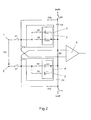
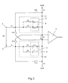
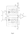
- FIG. 1 shows the circuit arrangement for the discharge all capacities, Fig. 2, the circuit arrangement accordingly 1, in which a transhipment or equal charge the capacitances is made, Fig. 3 the switch arrangement within the switches during the track phase and Fig. 4 the switch positions in the phase of successive approximation.
- the connections for the measuring voltage are designated 1 and 2, the measuring voltage Vin being applied to these connections.
- the connections can be separated from the CDACs 3 via switch S1, these switches having to be open when the capacitances Cl ... 2 k C1 are discharged or reloaded.
- the discharge takes place by connecting the two capacitance arrays 4 in parallel with the damping capacitance Cd, as a result of which all capacitances are charged equally.
- the switches S1 are open, the switches S2 are closed and the sample block switch S5 is also opened during the transfer.
- the two reference voltages Vref N and Vref P are also separated from the circuit arrangement by switch S3, switches S1b and S3b being closed for the purpose of parallel connection including the damping capacitances Cd.
- switch S5 ie the sample block switch, as shown in FIG. 2, it can be seen that short-circuit discharge is now possible, switches S1 and S3 remaining open and switches S1b, S3b, S2 and S5 are closed.
- the comparator at the two inputs of which the outputs of the capacitance arrays are connected, is designated 5 here and contains the required memory modules or latches.
- the individual capacitances of the capacitance arrays are indicated with Cl or multiples of Cl and are each controlled via separate switches, which in turn are divided as an array, which results in 3 triple T gates in the DAC.
- a possible integration of the switches S1 and Slb in the switch array of DAC 3 results in quadruple T-gates.
- the comparator due to the free choice of Vref P and Vref N. maintain a CMV value within the allowable CMR, where because of the free choice of Vref P and Vref N the measuring range and thus changed the choice of the conversion area as desired can be.
- Due to the fully differential circuit a high degree of stability against voltage peaks Switching operations achieved and by dispensing with a buffer and one derived from the input voltage to be measured CMV value can be the load on the voltage source to be measured be kept extremely low.
- the sampling rate be significantly increased since the loading time is no longer due such a buffer is limited. By that on the common ground is dispensed with as a voltage reference value overall reduced the susceptibility to failure, and thereby the Sensitivity further increased.
Landscapes
- Engineering & Computer Science (AREA)
- Theoretical Computer Science (AREA)
- Analogue/Digital Conversion (AREA)
Abstract
Description
Claims (5)
- Differentieller Analog-Digitalwandler mit geschalteten Kapazitäten und sukzessiver Approximation, bei welchem ein Komparator mit den Kapazitäten verbunden ist und binär gewichtete als Arrays geschaltete Kapazitäten bezüglich der Meßeingänge und der Anschlüsse an den Komparator symmetrisch angeordnet sind, dadurch gekennzeichnet, daß Schalter für die Gleichladung bzw. Kurzschlußentladung aller Kapazitäten vor der Einleitung einer Trackphase angeordnet sind, daß in der Phase der sukzessiven Approximation jede Kapazität wahlweise mit jeweils einer der Referenzspannungsquellen über Schalter verbindbar ist und daß die sukzessive Approximation symmetrisch zur aus den Referenzspannungen resultierenden CMV (Common Mode Spannung) ausgelegt ist.
- Differentieller Analog-Digitalwandler nach Anspruch 1, dadurch gekennzeichnet, daß der Sample-Block-Schalter in der Trackphase geschlossen ist und die komparatorseitigen Anschlüsse der Kapazitätsarrays unmittelbar miteinander verbindet, sodaß die symmetrisch angeordneten Kapazitätsarrays in Serie geschaltet mit den Meßeingängen verbunden sind.
- Differentieller Analog-Digitalwandler nach Anspruch 1 oder 2, dadurch gekennzeichnet, daß die komparatorseitigen Anschlüsse der Kapazitätsarrays in der Trackphase und der Phase der sukzessiven Approximation mit jeweils einer Referenzspannungsquelle unter Zwischenschaltung von Dämpfungskondensatoren über Schalter verbindbar sind.
- Differentieller Analog-Digitalwandler nach einem der Ansprüche 1 bis 3, dadurch gekennzeichnet, daß die Schalter zu Mehrfach-T-Gates, insbesondere Vierfach-T-Gates, als Arrays parallelgeschaltet aufgeteilt und angeordnet sind.
- Differentieller Analog-Digitalwandler nach einem der Ansprüche 1 bis 4, dadurch gekennzeichnet, daß der Sample-Schalter aus mehreren Schaltern besteht, wobei ein Schalter als Sample-Schalter dient und die restlichen Schalter die Komparator-Eingänge während der Track-Phase vom Cap-Array abtrennen und auf das Common Mode Potential der Referenzspannung legen.
Applications Claiming Priority (2)
| Application Number | Priority Date | Filing Date | Title |
|---|---|---|---|
| AT0071699U AT3853U1 (de) | 1999-10-15 | 1999-10-15 | Differentieller analog-digitalwandler |
| AT71699U | 1999-10-15 |
Publications (3)
| Publication Number | Publication Date |
|---|---|
| EP1093229A2 true EP1093229A2 (de) | 2001-04-18 |
| EP1093229A3 EP1093229A3 (de) | 2003-11-05 |
| EP1093229B1 EP1093229B1 (de) | 2006-06-14 |
Family
ID=3497939
Family Applications (1)
| Application Number | Title | Priority Date | Filing Date |
|---|---|---|---|
| EP00890303A Expired - Lifetime EP1093229B1 (de) | 1999-10-15 | 2000-10-06 | Differentieller Analog-Digitalwandler |
Country Status (3)
| Country | Link |
|---|---|
| EP (1) | EP1093229B1 (de) |
| AT (2) | AT3853U1 (de) |
| DE (1) | DE50012965D1 (de) |
Cited By (6)
| Publication number | Priority date | Publication date | Assignee | Title |
|---|---|---|---|---|
| DE10250584B4 (de) * | 2001-11-12 | 2005-08-25 | Nec Electronics Corp., Kawasaki | Differenzeingabe-A/D-Wandler |
| DE102005030562A1 (de) * | 2005-06-30 | 2007-01-04 | Infineon Technologies Ag | Sukzessiv approximierender Analog/Digital-Wandler |
| WO2007115710A1 (de) * | 2006-04-04 | 2007-10-18 | Austriamicrosystems Ag | Analog/digital-wandleranordnung und verfahren |
| US8059020B2 (en) | 2006-05-30 | 2011-11-15 | Austriamicrosystems Ag | Adjustable analogue-digital converter arrangement and method for analogue-to-digital conversion |
| CN112636757A (zh) * | 2020-12-25 | 2021-04-09 | 上海东软载波微电子有限公司 | 逐次逼近型模数转换器及其失调补偿方法 |
| CN113922820A (zh) * | 2021-12-15 | 2022-01-11 | 之江实验室 | 一种基于后台校准的间断式缓冲电路及模数转换器 |
Family Cites Families (3)
| Publication number | Priority date | Publication date | Assignee | Title |
|---|---|---|---|---|
| US4831381A (en) * | 1987-08-11 | 1989-05-16 | Texas Instruments Incorporated | Charge redistribution A/D converter with reduced small signal error |
| US4803462A (en) * | 1987-08-11 | 1989-02-07 | Texas Instruments Incorporated | Charge redistribution A/D converter with increased common mode rejection |
| US5920275A (en) * | 1996-09-09 | 1999-07-06 | Iowa State University Research Foundation, Inc. | Analog-to-digital converter using weighted capacitor array and interpolating comparator |
-
1999
- 1999-10-15 AT AT0071699U patent/AT3853U1/de not_active IP Right Cessation
- 1999-10-15 AT AT00890303T patent/ATE330365T1/de not_active IP Right Cessation
-
2000
- 2000-10-06 DE DE50012965T patent/DE50012965D1/de not_active Expired - Lifetime
- 2000-10-06 EP EP00890303A patent/EP1093229B1/de not_active Expired - Lifetime
Cited By (11)
| Publication number | Priority date | Publication date | Assignee | Title |
|---|---|---|---|---|
| DE10250584B4 (de) * | 2001-11-12 | 2005-08-25 | Nec Electronics Corp., Kawasaki | Differenzeingabe-A/D-Wandler |
| DE102005030562A1 (de) * | 2005-06-30 | 2007-01-04 | Infineon Technologies Ag | Sukzessiv approximierender Analog/Digital-Wandler |
| US7342530B2 (en) | 2005-06-30 | 2008-03-11 | Infineon Technologies Ag | Successive approximation analog/digital converter |
| DE102005030562B4 (de) * | 2005-06-30 | 2012-04-26 | Infineon Technologies Ag | Sukzessiv approximierender Analog/Digital-Wandler |
| WO2007115710A1 (de) * | 2006-04-04 | 2007-10-18 | Austriamicrosystems Ag | Analog/digital-wandleranordnung und verfahren |
| GB2451969A (en) * | 2006-04-04 | 2009-02-18 | Austriamicrosystems Ag | Analog/digital converter assembly and corresponding method |
| US7903018B2 (en) | 2006-04-04 | 2011-03-08 | Austriamicrosystems Ag | Analog/digital converter assembly and corresponding method |
| US8059020B2 (en) | 2006-05-30 | 2011-11-15 | Austriamicrosystems Ag | Adjustable analogue-digital converter arrangement and method for analogue-to-digital conversion |
| CN112636757A (zh) * | 2020-12-25 | 2021-04-09 | 上海东软载波微电子有限公司 | 逐次逼近型模数转换器及其失调补偿方法 |
| CN112636757B (zh) * | 2020-12-25 | 2024-05-31 | 上海东软载波微电子有限公司 | 逐次逼近型模数转换器及其失调补偿方法 |
| CN113922820A (zh) * | 2021-12-15 | 2022-01-11 | 之江实验室 | 一种基于后台校准的间断式缓冲电路及模数转换器 |
Also Published As
| Publication number | Publication date |
|---|---|
| EP1093229B1 (de) | 2006-06-14 |
| EP1093229A3 (de) | 2003-11-05 |
| DE50012965D1 (de) | 2006-07-27 |
| AT3853U1 (de) | 2000-08-25 |
| ATE330365T1 (de) | 2006-07-15 |
Similar Documents
| Publication | Publication Date | Title |
|---|---|---|
| DE69507023T2 (de) | Ladungswiederverteilung-ad-wandler mit systemeichung | |
| DE102017121491B4 (de) | Verfahren und Vorrichtung zum Reduzieren des Effekts dielektrischer Absorption in einem SAR-ADC | |
| DE19946750B4 (de) | Zweischritt-Analog-Digital-Wandler und -Verfahren | |
| DE102011110115B4 (de) | Vorrichtung und Verfahren zum Messen der DNL eines SAR ADC | |
| DE69313619T2 (de) | Schaltungsanordnung zur analog-digital umsetzung | |
| DE102013018971B4 (de) | Strang-Digital-Analog-Wandler-Schnellladungssystem und Verfahren | |
| DE69131099T2 (de) | Analog-digitalwandler | |
| DE102015121385B4 (de) | Kalibrierungstechniken für SAR-ADCs mit Reservoirkondensatoren auf-dem-Chip | |
| DE102007033689B4 (de) | Analog-Digital-Wandler mit sukzessivem Approximationsregister und großem Eingangsbereich | |
| DE112016003065B4 (de) | Verstärkungskalibrierung für AD-Wandler mit externer Referenz | |
| DE202012013712U1 (de) | Ladungsumverteilungs-Digital-Analog-Wandler | |
| DE3136783C2 (de) | Analog/Digital-Umsetzer | |
| DE69505515T2 (de) | Cmos-analog-digitalumwandler niedriger spannung | |
| DE102008035215A1 (de) | Elektronisches Bauelement und Verfahren zur Analog-Digital-Wandlung unter Verwendung von sukzessiver Approximation | |
| DE19732840A1 (de) | Pipeline-Analog-Digital-Wandler | |
| DE102007044592B4 (de) | Zyklischer Analog-Digital-Wandler | |
| DE102019112542B4 (de) | Reservoirkondensator-basierter analog-digital-wandler | |
| EP1603139A1 (de) | Vorrichtung und Verfahren zur Kompensation von Fehlern in einer Sample-und-hold-Schaltung | |
| WO2007115710A1 (de) | Analog/digital-wandleranordnung und verfahren | |
| DE102015121564B4 (de) | Asynchroner SAR-ADU mit binär skalierter Redundanz | |
| DE112018005717T5 (de) | Verfahren und Vorrichtung zur Offset-Korrektur in SAR-ADC mit DAC mit reduziertem Kondensator-Array | |
| DE69528169T2 (de) | Automatische kalibrierungsschaltung mit einer referenzskala für einen digital-analogen wandler | |
| DE69221961T2 (de) | Schaltung zur Korrektur von durch dielektrische Relaxation verursachte Fehler für Ladungswiederverteilung-AD-Wandler | |
| DE112018004698T5 (de) | Verfahren und vorrichtung zur unterstützung eines breiten eingangsgleichtaktbereichs in sar-adcs ohne zusätzliche aktive schaltung | |
| EP1093229B1 (de) | Differentieller Analog-Digitalwandler |
Legal Events
| Date | Code | Title | Description |
|---|---|---|---|
| PUAI | Public reference made under article 153(3) epc to a published international application that has entered the european phase |
Free format text: ORIGINAL CODE: 0009012 |
|
| AK | Designated contracting states |
Kind code of ref document: A2 Designated state(s): AT BE CH CY DE DK ES FI FR GB GR IE IT LI LU MC NL PT SE |
|
| AX | Request for extension of the european patent |
Free format text: AL;LT;LV;MK;RO;SI |
|
| PUAL | Search report despatched |
Free format text: ORIGINAL CODE: 0009013 |
|
| AK | Designated contracting states |
Kind code of ref document: A3 Designated state(s): AT BE CH CY DE DK ES FI FR GB GR IE IT LI LU MC NL PT SE |
|
| AX | Request for extension of the european patent |
Extension state: AL LT LV MK RO SI |
|
| 17P | Request for examination filed |
Effective date: 20031119 |
|
| AKX | Designation fees paid |
Designated state(s): AT BE CH CY DE DK ES FI FR GB GR IE IT LI LU MC NL PT SE |
|
| 17Q | First examination report despatched |
Effective date: 20050415 |
|
| GRAP | Despatch of communication of intention to grant a patent |
Free format text: ORIGINAL CODE: EPIDOSNIGR1 |
|
| GRAS | Grant fee paid |
Free format text: ORIGINAL CODE: EPIDOSNIGR3 |
|
| GRAA | (expected) grant |
Free format text: ORIGINAL CODE: 0009210 |
|
| AK | Designated contracting states |
Kind code of ref document: B1 Designated state(s): AT BE CH CY DE DK ES FI FR GB GR IE IT LI LU MC NL PT SE |
|
| PG25 | Lapsed in a contracting state [announced via postgrant information from national office to epo] |
Ref country code: IT Free format text: LAPSE BECAUSE OF FAILURE TO SUBMIT A TRANSLATION OF THE DESCRIPTION OR TO PAY THE FEE WITHIN THE PRESCRIBED TIME-LIMIT;WARNING: LAPSES OF ITALIAN PATENTS WITH EFFECTIVE DATE BEFORE 2007 MAY HAVE OCCURRED AT ANY TIME BEFORE 2007. THE CORRECT EFFECTIVE DATE MAY BE DIFFERENT FROM THE ONE RECORDED. Effective date: 20060614 Ref country code: NL Free format text: LAPSE BECAUSE OF FAILURE TO SUBMIT A TRANSLATION OF THE DESCRIPTION OR TO PAY THE FEE WITHIN THE PRESCRIBED TIME-LIMIT Effective date: 20060614 Ref country code: FI Free format text: LAPSE BECAUSE OF FAILURE TO SUBMIT A TRANSLATION OF THE DESCRIPTION OR TO PAY THE FEE WITHIN THE PRESCRIBED TIME-LIMIT Effective date: 20060614 |
|
| REG | Reference to a national code |
Ref country code: GB Ref legal event code: FG4D Free format text: NOT ENGLISH |
|
| REG | Reference to a national code |
Ref country code: CH Ref legal event code: EP |
|
| REG | Reference to a national code |
Ref country code: IE Ref legal event code: FG4D Free format text: LANGUAGE OF EP DOCUMENT: GERMAN |
|
| REF | Corresponds to: |
Ref document number: 50012965 Country of ref document: DE Date of ref document: 20060727 Kind code of ref document: P |
|
| RAP2 | Party data changed (patent owner data changed or rights of a patent transferred) |
Owner name: AUSTRIAMICROSYSTEMS AG |
|
| PG25 | Lapsed in a contracting state [announced via postgrant information from national office to epo] |
Ref country code: SE Free format text: LAPSE BECAUSE OF FAILURE TO SUBMIT A TRANSLATION OF THE DESCRIPTION OR TO PAY THE FEE WITHIN THE PRESCRIBED TIME-LIMIT Effective date: 20060914 Ref country code: DK Free format text: LAPSE BECAUSE OF FAILURE TO SUBMIT A TRANSLATION OF THE DESCRIPTION OR TO PAY THE FEE WITHIN THE PRESCRIBED TIME-LIMIT Effective date: 20060914 |
|
| PG25 | Lapsed in a contracting state [announced via postgrant information from national office to epo] |
Ref country code: ES Free format text: LAPSE BECAUSE OF FAILURE TO SUBMIT A TRANSLATION OF THE DESCRIPTION OR TO PAY THE FEE WITHIN THE PRESCRIBED TIME-LIMIT Effective date: 20060925 |
|
| PG25 | Lapsed in a contracting state [announced via postgrant information from national office to epo] |
Ref country code: MC Free format text: LAPSE BECAUSE OF NON-PAYMENT OF DUE FEES Effective date: 20061031 Ref country code: LI Free format text: LAPSE BECAUSE OF NON-PAYMENT OF DUE FEES Effective date: 20061031 Ref country code: CH Free format text: LAPSE BECAUSE OF NON-PAYMENT OF DUE FEES Effective date: 20061031 |
|
| NLT2 | Nl: modifications (of names), taken from the european patent patent bulletin |
Owner name: AUSTRIAMICROSYSTEMS AG Effective date: 20060906 |
|
| PG25 | Lapsed in a contracting state [announced via postgrant information from national office to epo] |
Ref country code: PT Free format text: LAPSE BECAUSE OF FAILURE TO SUBMIT A TRANSLATION OF THE DESCRIPTION OR TO PAY THE FEE WITHIN THE PRESCRIBED TIME-LIMIT Effective date: 20061114 |
|
| GBT | Gb: translation of ep patent filed (gb section 77(6)(a)/1977) |
Effective date: 20061030 |
|
| NLV1 | Nl: lapsed or annulled due to failure to fulfill the requirements of art. 29p and 29m of the patents act | ||
| ET | Fr: translation filed | ||
| PLBE | No opposition filed within time limit |
Free format text: ORIGINAL CODE: 0009261 |
|
| STAA | Information on the status of an ep patent application or granted ep patent |
Free format text: STATUS: NO OPPOSITION FILED WITHIN TIME LIMIT |
|
| 26N | No opposition filed |
Effective date: 20070315 |
|
| REG | Reference to a national code |
Ref country code: CH Ref legal event code: PL |
|
| REG | Reference to a national code |
Ref country code: FR Ref legal event code: CD |
|
| BERE | Be: lapsed |
Owner name: AUSTRIA MIKRO SYSTEME INTERNATIONAL A.G. Effective date: 20061031 |
|
| PG25 | Lapsed in a contracting state [announced via postgrant information from national office to epo] |
Ref country code: AT Free format text: LAPSE BECAUSE OF NON-PAYMENT OF DUE FEES Effective date: 20061006 |
|
| PG25 | Lapsed in a contracting state [announced via postgrant information from national office to epo] |
Ref country code: GR Free format text: LAPSE BECAUSE OF FAILURE TO SUBMIT A TRANSLATION OF THE DESCRIPTION OR TO PAY THE FEE WITHIN THE PRESCRIBED TIME-LIMIT Effective date: 20060915 |
|
| PG25 | Lapsed in a contracting state [announced via postgrant information from national office to epo] |
Ref country code: LU Free format text: LAPSE BECAUSE OF NON-PAYMENT OF DUE FEES Effective date: 20061006 |
|
| PG25 | Lapsed in a contracting state [announced via postgrant information from national office to epo] |
Ref country code: CY Free format text: LAPSE BECAUSE OF FAILURE TO SUBMIT A TRANSLATION OF THE DESCRIPTION OR TO PAY THE FEE WITHIN THE PRESCRIBED TIME-LIMIT Effective date: 20060614 |
|
| PGFP | Annual fee paid to national office [announced via postgrant information from national office to epo] |
Ref country code: IE Payment date: 20080829 Year of fee payment: 9 |
|
| PGFP | Annual fee paid to national office [announced via postgrant information from national office to epo] |
Ref country code: GB Payment date: 20080904 Year of fee payment: 9 |
|
| PG25 | Lapsed in a contracting state [announced via postgrant information from national office to epo] |
Ref country code: BE Free format text: LAPSE BECAUSE OF FAILURE TO SUBMIT A TRANSLATION OF THE DESCRIPTION OR TO PAY THE FEE WITHIN THE PRESCRIBED TIME-LIMIT Effective date: 20061031 |
|
| PG25 | Lapsed in a contracting state [announced via postgrant information from national office to epo] |
Ref country code: IE Free format text: LAPSE BECAUSE OF NON-PAYMENT OF DUE FEES Effective date: 20091006 |
|
| PG25 | Lapsed in a contracting state [announced via postgrant information from national office to epo] |
Ref country code: GB Free format text: LAPSE BECAUSE OF NON-PAYMENT OF DUE FEES Effective date: 20091006 |
|
| REG | Reference to a national code |
Ref country code: DE Ref legal event code: R082 Ref document number: 50012965 Country of ref document: DE Representative=s name: GODEMEYER BLUM LENZE PARTNERSCHAFT, PATENTANWA, DE Ref country code: DE Ref legal event code: R082 Ref document number: 50012965 Country of ref document: DE Representative=s name: GODEMEYER BLUM LENZE PATENTANWAELTE, PARTNERSC, DE |
|
| REG | Reference to a national code |
Ref country code: FR Ref legal event code: PLFP Year of fee payment: 16 |
|
| REG | Reference to a national code |
Ref country code: FR Ref legal event code: PLFP Year of fee payment: 17 |
|
| PGFP | Annual fee paid to national office [announced via postgrant information from national office to epo] |
Ref country code: IT Payment date: 20161024 Year of fee payment: 17 |
|
| REG | Reference to a national code |
Ref country code: FR Ref legal event code: PLFP Year of fee payment: 18 |
|
| REG | Reference to a national code |
Ref country code: FR Ref legal event code: PLFP Year of fee payment: 19 |
|
| PG25 | Lapsed in a contracting state [announced via postgrant information from national office to epo] |
Ref country code: IT Free format text: LAPSE BECAUSE OF NON-PAYMENT OF DUE FEES Effective date: 20171006 |
|
| PGFP | Annual fee paid to national office [announced via postgrant information from national office to epo] |
Ref country code: FR Payment date: 20181025 Year of fee payment: 19 |
|
| PGFP | Annual fee paid to national office [announced via postgrant information from national office to epo] |
Ref country code: DE Payment date: 20191121 Year of fee payment: 20 |
|
| REG | Reference to a national code |
Ref country code: DE Ref legal event code: R071 Ref document number: 50012965 Country of ref document: DE |
|
| PG25 | Lapsed in a contracting state [announced via postgrant information from national office to epo] |
Ref country code: FR Free format text: LAPSE BECAUSE OF NON-PAYMENT OF DUE FEES Effective date: 20191031 |