EP1093082A2 - Combination card having an IC chip module - Google Patents
Combination card having an IC chip module Download PDFInfo
- Publication number
- EP1093082A2 EP1093082A2 EP00307934A EP00307934A EP1093082A2 EP 1093082 A2 EP1093082 A2 EP 1093082A2 EP 00307934 A EP00307934 A EP 00307934A EP 00307934 A EP00307934 A EP 00307934A EP 1093082 A2 EP1093082 A2 EP 1093082A2
- Authority
- EP
- European Patent Office
- Prior art keywords
- module
- antenna
- antenna connection
- connection terminal
- terminal
- Prior art date
- Legal status (The legal status is an assumption and is not a legal conclusion. Google has not performed a legal analysis and makes no representation as to the accuracy of the status listed.)
- Granted
Links
Images






Classifications
-
- G—PHYSICS
- G06—COMPUTING OR CALCULATING; COUNTING
- G06K—GRAPHICAL DATA READING; PRESENTATION OF DATA; RECORD CARRIERS; HANDLING RECORD CARRIERS
- G06K19/00—Record carriers for use with machines and with at least a part designed to carry digital markings
- G06K19/06—Record carriers for use with machines and with at least a part designed to carry digital markings characterised by the kind of the digital marking, e.g. shape, nature, code
- G06K19/067—Record carriers with conductive marks, printed circuits or semiconductor circuit elements, e.g. credit or identity cards also with resonating or responding marks without active components
- G06K19/07—Record carriers with conductive marks, printed circuits or semiconductor circuit elements, e.g. credit or identity cards also with resonating or responding marks without active components with integrated circuit chips
- G06K19/077—Constructional details, e.g. mounting of circuits in the carrier
- G06K19/07745—Mounting details of integrated circuit chips
- G06K19/07747—Mounting details of integrated circuit chips at least one of the integrated circuit chips being mounted as a module
-
- G—PHYSICS
- G06—COMPUTING OR CALCULATING; COUNTING
- G06K—GRAPHICAL DATA READING; PRESENTATION OF DATA; RECORD CARRIERS; HANDLING RECORD CARRIERS
- G06K19/00—Record carriers for use with machines and with at least a part designed to carry digital markings
- G06K19/06—Record carriers for use with machines and with at least a part designed to carry digital markings characterised by the kind of the digital marking, e.g. shape, nature, code
- G06K19/067—Record carriers with conductive marks, printed circuits or semiconductor circuit elements, e.g. credit or identity cards also with resonating or responding marks without active components
- G06K19/07—Record carriers with conductive marks, printed circuits or semiconductor circuit elements, e.g. credit or identity cards also with resonating or responding marks without active components with integrated circuit chips
- G06K19/077—Constructional details, e.g. mounting of circuits in the carrier
- G06K19/07745—Mounting details of integrated circuit chips
-
- G—PHYSICS
- G06—COMPUTING OR CALCULATING; COUNTING
- G06K—GRAPHICAL DATA READING; PRESENTATION OF DATA; RECORD CARRIERS; HANDLING RECORD CARRIERS
- G06K19/00—Record carriers for use with machines and with at least a part designed to carry digital markings
- G06K19/06—Record carriers for use with machines and with at least a part designed to carry digital markings characterised by the kind of the digital marking, e.g. shape, nature, code
- G06K19/067—Record carriers with conductive marks, printed circuits or semiconductor circuit elements, e.g. credit or identity cards also with resonating or responding marks without active components
- G06K19/07—Record carriers with conductive marks, printed circuits or semiconductor circuit elements, e.g. credit or identity cards also with resonating or responding marks without active components with integrated circuit chips
- G06K19/077—Constructional details, e.g. mounting of circuits in the carrier
- G06K19/07749—Constructional details, e.g. mounting of circuits in the carrier the record carrier being capable of non-contact communication, e.g. constructional details of the antenna of a non-contact smart card
-
- G—PHYSICS
- G06—COMPUTING OR CALCULATING; COUNTING
- G06K—GRAPHICAL DATA READING; PRESENTATION OF DATA; RECORD CARRIERS; HANDLING RECORD CARRIERS
- G06K19/00—Record carriers for use with machines and with at least a part designed to carry digital markings
- G06K19/06—Record carriers for use with machines and with at least a part designed to carry digital markings characterised by the kind of the digital marking, e.g. shape, nature, code
- G06K19/067—Record carriers with conductive marks, printed circuits or semiconductor circuit elements, e.g. credit or identity cards also with resonating or responding marks without active components
- G06K19/07—Record carriers with conductive marks, printed circuits or semiconductor circuit elements, e.g. credit or identity cards also with resonating or responding marks without active components with integrated circuit chips
- G06K19/077—Constructional details, e.g. mounting of circuits in the carrier
- G06K19/07749—Constructional details, e.g. mounting of circuits in the carrier the record carrier being capable of non-contact communication, e.g. constructional details of the antenna of a non-contact smart card
- G06K19/07766—Constructional details, e.g. mounting of circuits in the carrier the record carrier being capable of non-contact communication, e.g. constructional details of the antenna of a non-contact smart card comprising at least a second communication arrangement in addition to a first non-contact communication arrangement
- G06K19/07769—Constructional details, e.g. mounting of circuits in the carrier the record carrier being capable of non-contact communication, e.g. constructional details of the antenna of a non-contact smart card comprising at least a second communication arrangement in addition to a first non-contact communication arrangement the further communication means being a galvanic interface, e.g. hybrid or mixed smart cards having a contact and a non-contact interface
-
- H—ELECTRICITY
- H05—ELECTRIC TECHNIQUES NOT OTHERWISE PROVIDED FOR
- H05K—PRINTED CIRCUITS; CASINGS OR CONSTRUCTIONAL DETAILS OF ELECTRIC APPARATUS; MANUFACTURE OF ASSEMBLAGES OF ELECTRICAL COMPONENTS
- H05K3/00—Apparatus or processes for manufacturing printed circuits
- H05K3/30—Assembling printed circuits with electric components, e.g. with resistors
- H05K3/32—Assembling printed circuits with electric components, e.g. with resistors electrically connecting electric components or wires to printed circuits
- H05K3/34—Assembling printed circuits with electric components, e.g. with resistors electrically connecting electric components or wires to printed circuits by soldering
- H05K3/341—Surface mounted components
- H05K3/3431—Leadless components
- H05K3/3436—Leadless components having an array of bottom contacts, e.g. pad grid array or ball grid array components
-
- H—ELECTRICITY
- H05—ELECTRIC TECHNIQUES NOT OTHERWISE PROVIDED FOR
- H05K—PRINTED CIRCUITS; CASINGS OR CONSTRUCTIONAL DETAILS OF ELECTRIC APPARATUS; MANUFACTURE OF ASSEMBLAGES OF ELECTRICAL COMPONENTS
- H05K1/00—Printed circuits
- H05K1/18—Printed circuits structurally associated with non-printed electric components
- H05K1/182—Printed circuits structurally associated with non-printed electric components associated with components mounted in printed circuit boards [PCB], e.g. insert-mounted components [IMC]
-
- H—ELECTRICITY
- H05—ELECTRIC TECHNIQUES NOT OTHERWISE PROVIDED FOR
- H05K—PRINTED CIRCUITS; CASINGS OR CONSTRUCTIONAL DETAILS OF ELECTRIC APPARATUS; MANUFACTURE OF ASSEMBLAGES OF ELECTRICAL COMPONENTS
- H05K2201/00—Indexing scheme relating to printed circuits covered by H05K1/00
- H05K2201/03—Conductive materials
- H05K2201/0332—Structure of the conductor
- H05K2201/0388—Other aspects of conductors
- H05K2201/0394—Conductor crossing over a hole in the substrate or a gap between two separate substrate parts
-
- H—ELECTRICITY
- H05—ELECTRIC TECHNIQUES NOT OTHERWISE PROVIDED FOR
- H05K—PRINTED CIRCUITS; CASINGS OR CONSTRUCTIONAL DETAILS OF ELECTRIC APPARATUS; MANUFACTURE OF ASSEMBLAGES OF ELECTRICAL COMPONENTS
- H05K2201/00—Indexing scheme relating to printed circuits covered by H05K1/00
- H05K2201/09—Shape and layout
- H05K2201/09209—Shape and layout details of conductors
- H05K2201/09372—Pads and lands
- H05K2201/09472—Recessed pad for surface mounting; Recessed electrode of component
-
- H—ELECTRICITY
- H05—ELECTRIC TECHNIQUES NOT OTHERWISE PROVIDED FOR
- H05K—PRINTED CIRCUITS; CASINGS OR CONSTRUCTIONAL DETAILS OF ELECTRIC APPARATUS; MANUFACTURE OF ASSEMBLAGES OF ELECTRICAL COMPONENTS
- H05K2201/00—Indexing scheme relating to printed circuits covered by H05K1/00
- H05K2201/10—Details of components or other objects attached to or integrated in a printed circuit board
- H05K2201/10431—Details of mounted components
- H05K2201/10439—Position of a single component
- H05K2201/10477—Inverted
-
- H—ELECTRICITY
- H05—ELECTRIC TECHNIQUES NOT OTHERWISE PROVIDED FOR
- H05K—PRINTED CIRCUITS; CASINGS OR CONSTRUCTIONAL DETAILS OF ELECTRIC APPARATUS; MANUFACTURE OF ASSEMBLAGES OF ELECTRICAL COMPONENTS
- H05K2201/00—Indexing scheme relating to printed circuits covered by H05K1/00
- H05K2201/10—Details of components or other objects attached to or integrated in a printed circuit board
- H05K2201/10613—Details of electrical connections of non-printed components, e.g. special leads
- H05K2201/10621—Components characterised by their electrical contacts
- H05K2201/10666—Plated through-hole for surface mounting on PCB
-
- H—ELECTRICITY
- H05—ELECTRIC TECHNIQUES NOT OTHERWISE PROVIDED FOR
- H05K—PRINTED CIRCUITS; CASINGS OR CONSTRUCTIONAL DETAILS OF ELECTRIC APPARATUS; MANUFACTURE OF ASSEMBLAGES OF ELECTRICAL COMPONENTS
- H05K3/00—Apparatus or processes for manufacturing printed circuits
- H05K3/30—Assembling printed circuits with electric components, e.g. with resistors
- H05K3/32—Assembling printed circuits with electric components, e.g. with resistors electrically connecting electric components or wires to printed circuits
- H05K3/321—Assembling printed circuits with electric components, e.g. with resistors electrically connecting electric components or wires to printed circuits by conductive adhesives
-
- H—ELECTRICITY
- H10—SEMICONDUCTOR DEVICES; ELECTRIC SOLID-STATE DEVICES NOT OTHERWISE PROVIDED FOR
- H10W—GENERIC PACKAGES, INTERCONNECTIONS, CONNECTORS OR OTHER CONSTRUCTIONAL DETAILS OF DEVICES COVERED BY CLASS H10
- H10W72/00—Interconnections or connectors in packages
- H10W72/50—Bond wires
- H10W72/531—Shapes of wire connectors
- H10W72/536—Shapes of wire connectors the connected ends being ball-shaped
-
- H—ELECTRICITY
- H10—SEMICONDUCTOR DEVICES; ELECTRIC SOLID-STATE DEVICES NOT OTHERWISE PROVIDED FOR
- H10W—GENERIC PACKAGES, INTERCONNECTIONS, CONNECTORS OR OTHER CONSTRUCTIONAL DETAILS OF DEVICES COVERED BY CLASS H10
- H10W72/00—Interconnections or connectors in packages
- H10W72/50—Bond wires
- H10W72/531—Shapes of wire connectors
- H10W72/5363—Shapes of wire connectors the connected ends being wedge-shaped
-
- H—ELECTRICITY
- H10—SEMICONDUCTOR DEVICES; ELECTRIC SOLID-STATE DEVICES NOT OTHERWISE PROVIDED FOR
- H10W—GENERIC PACKAGES, INTERCONNECTIONS, CONNECTORS OR OTHER CONSTRUCTIONAL DETAILS OF DEVICES COVERED BY CLASS H10
- H10W90/00—Package configurations
- H10W90/701—Package configurations characterised by the relative positions of pads or connectors relative to package parts
- H10W90/751—Package configurations characterised by the relative positions of pads or connectors relative to package parts of bond wires
- H10W90/754—Package configurations characterised by the relative positions of pads or connectors relative to package parts of bond wires between a chip and a stacked insulating package substrate, interposer or RDL
-
- Y—GENERAL TAGGING OF NEW TECHNOLOGICAL DEVELOPMENTS; GENERAL TAGGING OF CROSS-SECTIONAL TECHNOLOGIES SPANNING OVER SEVERAL SECTIONS OF THE IPC; TECHNICAL SUBJECTS COVERED BY FORMER USPC CROSS-REFERENCE ART COLLECTIONS [XRACs] AND DIGESTS
- Y02—TECHNOLOGIES OR APPLICATIONS FOR MITIGATION OR ADAPTATION AGAINST CLIMATE CHANGE
- Y02P—CLIMATE CHANGE MITIGATION TECHNOLOGIES IN THE PRODUCTION OR PROCESSING OF GOODS
- Y02P70/00—Climate change mitigation technologies in the production process for final industrial or consumer products
- Y02P70/50—Manufacturing or production processes characterised by the final manufactured product
Definitions
- the present invention generally relates to an IC card and, more particularly, to a combination card which can exchange data with an external device by both a contacting method and a non-contacting method.
- a contacting method an IC card having terminals exposed on a surface thereof is used.
- the terminals of the external device are made in contact with the terminals of the IC card and are electrically connected thereto so that data exchange can be performed between the IC card and the external device.
- an IC card provided with an antenna inside thereof is used.
- data exchange is performed by radio communication between the IC card and the IC card reader.
- Relatively simple data is exchanged by the non-contacting method. For example, data used for an attestation of an ID number in a security system may be exchanged by the non-contacting method.
- the combination card which is an IC card that can be used by both the contacting method and the non-contacting method. That is, the combination card is an IC card provided with both the connection terminals for exchanging data by the contacting method and an antenna for exchanging data by the non-contacting method.
- FIG. 1 is a plan view of a conventional combination card.
- the conventional combination card comprises a card body 1 and an IC card module 2 (hereinafter simply referred to as a module) incorporated in the card body 1.
- the card body 1 is made of a plastic material.
- a loop antenna 3 is incorporated in the card body 1.
- a plurality of external connection terminals (electrodes) 4 are formed on one side of the module.
- the module 2 is incorporated in the card body 1 so that the external connection terminals 4 are exposed on the surface of the card body 1.
- the surface on which the external connection terminals 4 are exposed is referred to as a terminal surface.
- Antenna terminals 5 are provided on a side of the module 2 opposite to the terminal surface. Opposite ends of the antenna 3 are connected to the antenna connection terminals 5.
- the surface opposite to the terminal surface of the module 2 is referred to as a mounting surface.
- FIG. 2 is a plan view of the terminal surface of the module 2.
- FIG. 3 is a plan view of the mounting surface of the module 2.
- the module 2 comprises a circuit substrate 7 and an IC chip 8 (refer to FIG. 4) mounted on the circuit substrate 7.
- a plurality of external connection terminals (electrodes) 4 are formed on the terminal surface of the module 2.
- the external connection terminals 4 are formed by patterning a copper plate applied to the circuit substrate 7 by etching. It should be noted that the area indicated by double dashed chain lines in the center of each of the external connection terminals 4 in FIG. 2 corresponds to an effective are of each of the external connection terminals 4.
- the IC chip 8 is mounted on the mounting surface of the module 2, and is encapsulated by seal resin.
- Antenna connection terminals 5 are formed on the mounting surface outside the seal resin 9.
- FIG. 4 is a plan view of the module 2 before the IC chip 8 is encapsulated by the seal resin 9.
- the IC chip 8 is mounted on the center of the circuit substrate 7.
- the electrodes of the IC chip 8 are connected to respective lead wires 10 formed on the mounting surface of the circuit substrate 7 by bonding wires 11, respectively.
- the lead wires 10 are electrically connected to the respective external connection terminals 4 on the terminal surface of the circuit substrate 7 via respective through holes 12.
- the card body 1 is previously provided with antenna 3.
- a recess 1a is formed in a predetermined portion of the card body 1. Opposite ends of the antenna 3 are exposed in the vicinity of the recess 1a so that the antenna connection terminals of the module 2 are connected thereto.
- solder 13 is applied onto the antenna connection terminals 5 of the module 2. Then, the module 2 is assembled to the card body 1 so that the seal resin 9 fits in the recess 1a of the card body 1. At this time, the solder 13 on the antenna connection terminals 5 contacts the opposite ends of the antenna 3. In this state, a heating jig (solder iron) is pressed from the terminal surface side of the module 2 so as to melt the solder 13 by heat from the heating jig o connect the antenna connection terminals 5 and the ends of the antenna 3 to each other.
- a heating jig solder iron
- the heating jig is configured and arranged to locally heat a portion corresponding to the antenna connection terminals 5 so that the heat provided by the heating jig is not transmitted to the IC chip 8 as much as possible. Additionally, since the card body 1 is formed of a plastic material having a relatively low heat resistance, the heating temperature must be controlled so that the temperature of the solder 13 does not exceed the melting point of the solder too much.
- FIG. 6 is a side view of the module 2 for explaining the process of incorporating the module 2 into a sheet provided with antenna.
- the antenna 3 is applied to the sheet 14.
- the sheet 14 is provided with an opening 14a in which the seal resin 9 of the module 2 is fitted.
- the heating jig shown in FIG. 6 is also configured and arranged to locally heat a portion corresponding to the antenna connection terminals 5. Additionally, since the sheet 14 is formed of a material having a relatively low heat resistance, the heating temperature must be controlled so that the temperature of the solder 13 does not exceed the melting point of the solder too much.
- a more specific object of the present invention is to provide a module of a combination card, which module can be incorporated into a card body with solder being easily melted and heat transmission to portions other than the antenna connection terminals being reduced.
- a combination card comprising: a card body provided with an antenna; and a module including a substrate which has a terminal surface on which at least one external connection terminal is formed and a mounting surface opposite to the terminal surface, an IC chip being mounted on the mounting surface, wherein said module includes at least one antenna connection terminal located on the mounting surface, the antenna connection terminal being connected to the antenna, and at least a part of the antenna connection terminal is exposed on the terminal surface.
- the antenna connection terminal is connected to the antenna by a solder (or a silver paste). That is, the soldering is performed by melting the solder applied to the antenna connection terminal exposed on the mounting surface by pressing a heating jig against the antenna connection terminal exposed on the terminal surface. Accordingly, if the antenna connection terminal has a part exposed on the terminal surface, heat can be transmitted from the heating jig to the solder by passing through only the antenna connection terminal by pressing the heating jig against the exposed part of the antenna connection terminal. Thus, the solder is efficiently heated, and the temperature of the heating jig and the heating time van be reduced. Therefore, the card body and the IC chip mounted on the mounting surface can be prevented from being influenced by the heat from the heating jig.
- the antenna connection terminal may be separated from the external connection terminal.
- the heating jig can be made in contact with only the antenna connection terminal formed on the mounting surface of the module. Since the antenna connection terminal is separated from the external connection terminal formed on the terminal surface, the heat supplied to the antenna connection terminal does not transmit to the external connection terminal via a metal part. Accordingly, the heat from the heating jig does not transmit to other parts such as the IC chip on the substrate via the external connection terminal.
- the antenna connection terminal may include a first antenna connection terminal formed on the terminal surface and a second antenna connection terminal formed on the mounting surface, and the first antenna connection terminal is electrically connected to the second antenna connection terminal via a through hole having a metal plated inner surface.
- the heat transmitted from the heating jig to the first antenna connection terminal reaches the second antenna connection terminal by transmitting the metal plated portion of the inner surface of the through hole. That is, the heat from the heating jig reaches the solder by transmitting a metal part.
- the heat from the heating jig transmits from the antenna connection terminal to the solder via the substrate.
- the heat from the heating jig transmits to the solder faster and more efficiently than the conventional module. Accordingly, the temperature of the heating jig can be set lower than that of the conventional module, and the heating time can be reduced.
- an amount of heat transmitted to portions other than the solder can be reduced, which prevents the card body from being deformed due to the heat. Additionally, since the amount of heat transmitted from the heating jig to the IC chip is reduced when the heating time is short, the temperature rise of the IC chip can also be reduced.
- a state of soldered portion can be checked by observing inside of the through hole after the soldering process is completed. Thus, a reliable soldering can be performed. Further, if the amount of solder is in excess, the excessive solder does not spread around the antenna connection terminal and is filled in the through hole. Accordingly, the antenna connection terminal is prevented from short-circuiting due to the excessive solder. Additionally, even if an appropriate amount of the solder is applied to the antenna connection terminal, some amount of the melted solder is filled in the through hole. Thereby, the soldered area is increased, and eth strength of soldered portion is increased.
- the antenna connection terminal may be formed on the mounting surface, and at least one conductive bonding member may extend between the terminal surface and the mounting surface by passing through the substrate of the module so as to connect the antenna connection terminal to the antenna.
- an IC card module configured and arranged to be used in a combination card, the IC card module comprising: a substrate having a terminal surface on which at least one external connection terminal is formed and a mounting surface opposite to the terminal surface; an IC chip mounted on the mounting surface; and at least one antenna connection terminal connected to an antenna provided in the combination card, at least a part of the antenna connection terminal being exposed on the terminal surface of the substrate.
- a manufacturing method of a combination card provided with an IC card module incorporated into a flat member provided with an antenna comprising the steps of: applying an electrically conductive bonding material onto at least one antenna connection terminal provided in the IC card module; placing the IC card module in a predetermined position on the flat member; and bonding the antenna connection terminal to the antenna by the electrically conductive bonding material by heating said antenna connection terminal exposed on the terminal surface of said IC card module.
- FIG. 7 is a plan view of a terminal surface of a module used in a combination card according to the first embodiment of the present invention.
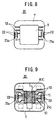
- FIG. 8 is a plan view of a mounting surface of the module shown in FIG. 7. It should be noted that, in FIGS. 7 to 11, parts that are the same as the parts shown in FIGS. 1 to 5 are given the same reference numerals, and descriptions thereof will be omitted.
- the combination card according to the first embodiment of the present invention comprises the card body 1 shown in FIG. 1 and a module 20 shown in FIGS. 7 to 9. That is, the module 20 is incorporated into the card body 1, and the terminal surface thereof is exposed on the surface of the card body 1.
- the module 20 comprises the circuit substrate 7 and the IC chip mounted on the circuit substrate 7. As shown in FIG. 7, a plurality of flat external connection terminals (electrodes) 4 are formed on the terminal surface of the module 20. Unlike the conventional module 2, an antenna connection terminal 21b is formed in a portion corresponding to an antenna connection terminal 21a of the mounting surface. The antenna connection terminal 21b and the external connection terminals 4 are formed by patterning a copper plate applied to the circuit substrate 7 by etching. It should be noted that, an area indicated by a double dashed chain line in each of the external connection terminals 4 in FIG. 7 corresponds to an effective area of each of the external connection terminals 4.
- the IC chip 8 is mounted on the mounting surface of the module 20, and is encapsulated by the seal resin 9. As mentioned above, the antenna connection terminal 21a is formed on the mounting surface outside the seal resin 9.
- FIG. 9 is a plan view of the module 20 before the IC chip 8 is encapsulated by the seal resin 9.
- the IC chip 8 is mounted in the center of the circuit substrate 7.
- the electrodes of the IC chip 8 are connected to the lead wires 10 formed on the mounting surface of the circuit substrate 7 by the bonding wires 11.
- the lead wires 10 are electrically connected to respective external connection terminals 4 on the terminal surface via respective through holes 12.
- FIG. 10 is an enlarged cross-sectional view of an area adjacent to the antenna connection terminals 21a and 21b of the module 20. As shown in FIG. 10, a plurality of through holes 22 are provided between each of the antenna connection terminals 21a formed on the mounting surface and the respective one of the antenna connection terminals 21b formed on the terminal surface.
- each of the through holes 22 is metal (gold) plated similar to the conventional through hole such as the through hole 12 provided between the lead wires 10 and the external connection terminals 4. Accordingly, the through holes 22 can be formed in the same process as the through holes 12. However, in the present embodiment, the through holes 22 provided between the antenna connection terminals 21a and 21b is not used to provide an electrical connection but is used to transmit a heat. That is, the plating layer 22a on an inner wall of each of the through holes 22 facilitates the heat transmission from the antenna connection terminals 21b to the antenna connection terminals 21a.
- six through holes 22 are provided to one antenna connection terminal 21a over the entire surface of the antenna connection terminal 21a.
- the card body 1 is previously provided with antenna 3.
- the recess 1a is formed in a predetermined portion of the card body 1. Opposite ends of the antenna 3 are exposed in the vicinity of the recess 1a so that the antenna connection terminal 21a of the module 20 is soldered thereto.
- solder 23 is applied onto each of the antenna connection terminals 21a on the mounting surface of the module 20. Then, the module 20 is assembled to the card body 1 so that the seal resin 9 fits in the recess 1a of the card body 1. At this time, the solder 23 on each of the antenna connection terminals 21a contacts the respective opposite end of the antenna 3. In this state, a heating jig (solder iron) is pressed against the antenna connection terminals 21b formed on the terminal surface of the module 20 so as to melt the solder 23 by the heat from the heating jig to connect the antenna connection terminals 21a to the respective ends of the antenna 3. It should be noted that a conductive bonding material such as a silver paste may be used instead of paste solder 23.
- the heat transmitted from the heating jig to the antenna connection terminal 21b reaches the antenna connection terminal 21a on the opposite side by transmitting through the plating part on an inner surface of the through holes 22. That is, the heat form the heating jig is transmitted to the solder 23 via a metal portion.
- the heat form the hating jig is transmitted from the antenna connection terminal 5 to the solder. Accordingly, in the module 20 according to the present embodiment, the heat from the heating jig is transmitted to the solder 23 more quickly and efficiently than the conventional module 2.
- the temperature of the heating jig can be set lower than the conventional one, and the heating time can be reduced.
- the short heating time reduces an amount of heat transmitted from the heating jig to the IC chip 8, a temperature rise of the IC chip 8 can be reduces.
- the heating jig contacts only the antenna connection terminals 21b formed on the terminal surface of the module 20.
- the antenna connection terminals 21bare separated from the external connection terminals 4, and the heat supplied to the antenna connection terminals 21b does not directly transmit to the external connection terminals 4. That is, the heat supplied to the antenna connection terminals 21b does not transmit to the antenna connection terminals 21b via a metal portion. Accordingly, the heat of the heating jig cannot transmit to the IC chip 8 through a metal part such as the external connection terminal 4. Thus, a bad influence due to the temperature rise in the IC chip 8 during the soldering process can be reduced.
- a plurality of thorough holes 22 are provided to each of the antenna connection terminals 21b, and, thus, the state of the soldered portion can be checked by visually inspecting inside the through holes 22. Accordingly, a reliable soldering can be achieved.
- a plurality of through holes 22 are provided, a single though hole may provide a similar effect.
- the terminals are prevented from short-circuiting to each other.
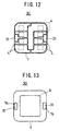
- FIG. 12 is a plan view of a terminal surface of a module used in a combination card according to the second embodiment of the present invention.
- FIG. 13 is a plan view of the module shown in FIG. 12. It should be noted that in FIGS. 12 through 16, parts that are the same as the parts shown in FIGS. 1 through 5 are given the same reference numerals.
- the combination card according to the second embodiment of the present invention comprises the card body 1 shown in FIG. 1 and the module 30 shown in FIGS. 12 through 16. That is, the module 30 is incorporated into the card body 1, the terminal surface of the module 30 is exposed on the surface of the card body 1.
- the module 30 comprises the circuit substrate 7 and the IC chip 8 (refer to FIG. 14) mounted on the circuit substrate 7.
- a plurality of flat external connection terminals (electrodes) 4 are formed on the terminal surface of the module 30.
- antenna connection terminals 31 are formed on the terminal surface of the module 30.
- the antenna connection terminals 31 and the external connection terminals 4 are formed by patterning a copper plate applied to the circuit substrate 7 by etching. Portions of the circuit substrate 7 corresponding to the antenna connection terminals 31 are provided with openings 7a as shown in FIG. 13.
- the antenna connection terminals 31 are exposed on the mounting surface. It should be noted that in FIG. 2, an area indicated by a double dashed chain line corresponds to an effective area of each of the external connection terminals 4.
- the IC chip 8 is mounted on the mounting surface of the module 30, and is encapsulated by a real resin 9. No circuit pattern is formed on the mounting surface of the module 30. That is, the electrodes of the IC chip 8 are directly connected to the external connection terminals 4 and the antenna connection terminals 31.
- FIG. 14 is a plan view of the module 30 before the IC chip 8 is encapsulated by the seal resin 9.
- the IC chip 8 is mounted in the center of the circuit substrate 7, and an opening 7b is formed at a position corresponding to each of the external connection terminals 4 and the antenna connection terminals 31.
- the electrodes of the IC chip 8 are electrically connected to the respective external connection terminals 4 and the antenna connection terminals 31 via bonding wires.
- the seal resin 9 is provided so as to encapsulate the IC chip 8 and the openings 7b.
- FIG. 15 is an enlarged cross-sectional view of a portion including the antenna connection terminal 31 and the opening 7b of the module 30.
- the module 30 is constituted by a single-side copper applied substrate. That is, a copper plate is applied to one side of the circuit substrate 7 so that the external connection terminals 4 and the antenna connection terminals 31 are formed by etching the copper plate.
- the external connection terminals 4 and the antenna connection terminals 31 are exposed on the side of the mounting surface through the openings 7a and 7b.
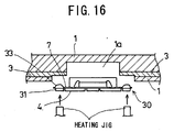
- a solder 33 can be supplied from the side of the mounting surface to the antenna connection terminals 31.
- the bonding wires 11 can be connected to the external connection terminals 4 and the antenna connection terminals 31 from the side of the mounting surface.
- the antenna 3 is previously embedded in the card body 1. Additionally, the recess 1a, which receives the seal resin 9, is provided in a predetermined portion of card body 11. The opposite ends of the antenna 3 expose in the vicinity of the recess 1a.
- the antenna terminals 31 of the module 30 are connected to the opposite ends of the antenna 3, respectively, by a conductive bonding material such as a solder or a silver paste. In the present embodiment, a solder is used.
- the paste solder 33 is applied to the antenna connection terminals 31 of the module 30 from the side of the mounting surface through the openings 7a.
- the module 30 is incorporated into the card body 1 so that the seal resin 9 fits in the recess 1a of the card body 1.
- the solder 33 on each of the antenna connection terminals 31 contacts the respective one of the ends of the antenna 3.
- the heating jig soldder iron
- the antenna connection terminals 31 formed on the terminal surface of the module 30 so as to melt the solder 33 by the heat from the heating jig and solder the antenna connection terminals 31 and the ends of the antenna 3.
- FIG. 17 is an illustration for explaining a process of incorporating the module 30 into the sheet 14 provided with antenna.
- the antenna 3 is previously provided in the sheet 14. Additionally, an opening, which receives the seal resin 9, is provided in a predetermined position of the sheet 14.
- the antenna connection terminals 31 of the module 30 are bonded by a conductive bonding material such as a solder or a silver paste. In the present embodiment, a solder is used.
- a paste solder 33 is applied to the antenna connection terminals 31 of the module 30 from the side of the mounting surface through the openings 7a.
- the module 30 is incorporated into the card body 1 so that the seal resin 9 fits in the recess 14a of the sheet 14.
- the solder 33 on each of the antenna connection terminals 31 contacts the respective one of the ends of the antenna 3.
- the heating jig soldder iron
- the antenna connection terminals 31 formed on the terminal surface of the module 30 so as to melt the solder 33 by the heat from the heating jig and solder the antenna connection terminals 31 and the ends of the antenna 3.
- a heat supplied by the heating jig to the antenna connection terminals 31 directly transmits to the solder 33.
- a heat supplied by the heating jig reaches the solder by transmitting through the circuit substrate 7 and the antenna connection terminals 5.
- the heat from the heating jig can be more rapidly and efficiently transmitted to the solder 33 than the conventional module 2.
- the temperature of the heating jig can be set lower than the conventional one.
- a heat transmitting to portions other than the solder 33 can be reduced, which prevent the card body 1 or the sheet 14 from deforming due to the heat.
- an amount of heat transmitted from the heating jig to the IC chip 8 is reduced. Thereby, a temperature rise of the IC chip 8 can be reduced.
- the heating jig contacts only the antenna connection terminals 31 formed on the terminal surface of the module 30.
- the antenna connection terminals 31 are separated from the external Connection terminals 4 formed on the terminal surface.
- the heat supplied to the antenna connection terminals 31 do not directly transmit to the external connection terminals 4, that is, the heat does not transmits to the external connection terminals 4 through a metal portion.
- the heat does not transmit to the IC chip 8 through the external connection terminals 4 as is in the conventional module 2.
- an undesirable influence to the IC chip 8 due to a temperature rise can be further reduced.
- the module 30 since the module 30 is produced by a substrate with a copper plate on a single side, the module 30 can be produced at a lower cost than the conventional module 2.
Landscapes
- Engineering & Computer Science (AREA)
- Microelectronics & Electronic Packaging (AREA)
- Computer Hardware Design (AREA)
- Physics & Mathematics (AREA)
- General Physics & Mathematics (AREA)
- Theoretical Computer Science (AREA)
- Manufacturing & Machinery (AREA)
- Credit Cards Or The Like (AREA)
- Manufacturing Of Electrical Connectors (AREA)
- Connections Effected By Soldering, Adhesion, Or Permanent Deformation (AREA)
Abstract
Description
Claims (8)
- A combination card comprising:a card body (1) provided with an antenna (3); anda module (20, 30) including a substrate (7) which has a terminal surface on which at least one external connection terminal (4) is formed and a mounting surface opposite to the terminal surface, an IC chip (8) being mounted on the mounting surface,
characterized in that:said module (20) includes at least one antenna connection terminal located on the mounting surface, the antenna connection terminal being connected to said antenna (3), and at least a part of said antenna connection terminal is exposed on said terminal surface. - The combination card as claimed in claim 1, characterized in that said antenna connection terminal (21b, 31) is separated from said external connection terminal (4).
- The combination card as claimed in claim 1, characterized in that said antenna connection terminal includes a first antenna connection terminal (21b) formed on said terminal surface and a second antenna connection terminal (21a) formed on said mounting surface, and said first antenna connection terminal (21b) is electrically connected to said second antenna connection terminal (21a) via a through hole (22) having a metal plated inner surface.
- The combination card as claimed in claim 2, characterized in that said antenna connection terminal includes a first antenna connection terminal (21b) formed on said terminal surface and a second antenna connection terminal (21a) formed on said mounting surface, and said first antenna connection terminal (21b) is electrically connected to said second antenna connection terminal (21a) via a through hole (22) having a metal plated inner surface.
- The combination card as claimed in claim 1, characterized on that said antenna connection terminal (31) is formed on said mounting surface, and at least one conductive bonding member (33) extends between said terminal surface and said mounting surface by passing through said substrate (7) of said module (30) so as to connect said antenna connection terminal (31) to said antenna (3).
- The combination card as claimed in claim 2, characterized on that said antenna connection terminal (31) is formed on said mounting surface, and at least one conductive bonding member (33) extends between said terminal surface and said mounting surface by passing through said substrate (7) of said module (30) so as to connect said antenna connection terminal (31) to said antenna (3).
- An IC card module configured and arranged to be used in a combination card, the IC card module comprising:a substrate (7) having a terminal surface on which at least one external connection terminal (4) is formed and a mounting surface opposite to the terminal surface; andan IC chip (8) mounted on said mounting surface,
characterized in that:at least one antenna connection terminal connected to an antenna provided in said combination card, at least a part of said antenna connection terminal (21b, 31) being exposed on said terminal surface of said substrate (7). - A manufacturing method of a combination card provided with an IC card module (20, 30) incorporated into a flat member (1, 14) provided with an antenna (3), the manufacturing method characterize in the steps of:applying an electrically conductive bonding material (23, 33) onto at least one antenna connection terminal (21a, 31) provided in said IC card module;placing said IC card module in a predetermined position on said flat member; andbonding said antenna connection terminal to said antenna (3) by the electrically conductive bonding material by heating said antenna connection terminal (21b, 31) exposed on said terminal surface of said IC card module.
Applications Claiming Priority (2)
| Application Number | Priority Date | Filing Date | Title |
|---|---|---|---|
| JP28993699 | 1999-10-12 | ||
| JP28993699A JP4299414B2 (en) | 1999-10-12 | 1999-10-12 | Combination card, IC card module, and combination card manufacturing method |
Publications (3)
| Publication Number | Publication Date |
|---|---|
| EP1093082A2 true EP1093082A2 (en) | 2001-04-18 |
| EP1093082A3 EP1093082A3 (en) | 2002-06-12 |
| EP1093082B1 EP1093082B1 (en) | 2012-12-26 |
Family
ID=17749672
Family Applications (1)
| Application Number | Title | Priority Date | Filing Date |
|---|---|---|---|
| EP00307934A Expired - Lifetime EP1093082B1 (en) | 1999-10-12 | 2000-09-13 | Combination card having an IC chip module |
Country Status (3)
| Country | Link |
|---|---|
| US (1) | US6460773B1 (en) |
| EP (1) | EP1093082B1 (en) |
| JP (1) | JP4299414B2 (en) |
Cited By (8)
| Publication number | Priority date | Publication date | Assignee | Title |
|---|---|---|---|---|
| US6460773B1 (en) * | 1999-10-12 | 2002-10-08 | Fujitsu Limited | Combination card having an IC chip module |
| EP1532742A4 (en) * | 2002-08-12 | 2008-06-11 | Infotrust Inc | A battery pack having a dual-type smart card interface |
| DE102007048237A1 (en) * | 2007-10-08 | 2009-04-09 | Giesecke & Devrient Gmbh | Chip module for chip card |
| FR2940697A1 (en) * | 2008-12-26 | 2010-07-02 | Oberthur Technologies | Label for microchip card i.e. dual interface smart card, has adaptation unit adapting connection zone to two electrical connection configurations so that electronic component is connected to connection zone along one of configurations |
| WO2011154062A1 (en) * | 2010-06-08 | 2011-12-15 | Johnson Controls Technology Company | Electric connection between a supporting element and an electric element, method for making an electric connection, supporting element and electric element |
| EP2711873A4 (en) * | 2011-05-16 | 2014-11-05 | Ick Corp | Card using detonator and method for manufacturing same |
| WO2017191414A1 (en) * | 2016-05-06 | 2017-11-09 | Linxens Holding | Method for manufacturing chip cards and chip card obtained by said method |
| WO2021014080A1 (en) * | 2019-07-22 | 2021-01-28 | Idemia France | Electronic document module comprising a chip and a contact interface with an antenna connected to an i/o port of the chip, electronic document comprising such a module and method for checking a connection between the module and a corresponding antenna |
Families Citing this family (30)
| Publication number | Priority date | Publication date | Assignee | Title |
|---|---|---|---|---|
| JP4239352B2 (en) * | 2000-03-28 | 2009-03-18 | 株式会社日立製作所 | Manufacturing method of electronic device |
| JP2002342731A (en) * | 2001-05-16 | 2002-11-29 | Matsushita Electric Ind Co Ltd | Composite IC card |
| KR20020011361A (en) * | 2001-12-27 | 2002-02-08 | 최완균 | Integrated Circuit Card and Circuit Board Suitable For Use in the IC Card |
| AU2003223130A1 (en) * | 2002-09-03 | 2004-03-29 | 3B System, Inc. | Combination-type ic card and method of manufacturing the combination-type ic card |
| JP4241147B2 (en) * | 2003-04-10 | 2009-03-18 | ソニー株式会社 | IC card manufacturing method |
| JP2006119983A (en) * | 2004-10-22 | 2006-05-11 | Renesas Technology Corp | IC card and manufacturing method thereof |
| JP2007183776A (en) * | 2006-01-06 | 2007-07-19 | Renesas Technology Corp | Semiconductor device |
| JP4929930B2 (en) * | 2006-08-31 | 2012-05-09 | 凸版印刷株式会社 | Antenna sheet, IC inlet, and information recording medium |
| JP4961920B2 (en) * | 2006-09-13 | 2012-06-27 | 凸版印刷株式会社 | Manufacturing method of dual interface card |
| US7980477B2 (en) * | 2007-05-17 | 2011-07-19 | Féinics Amatech Teoranta | Dual interface inlays |
| US8030746B2 (en) * | 2008-02-08 | 2011-10-04 | Infineon Technologies Ag | Integrated circuit package |
| US8991712B2 (en) | 2010-08-12 | 2015-03-31 | Féinics Amatech Teoranta | Coupling in and to RFID smart cards |
| US8789762B2 (en) | 2010-08-12 | 2014-07-29 | Feinics Amatech Teoranta | RFID antenna modules and methods of making |
| USD686214S1 (en) * | 2011-07-28 | 2013-07-16 | Lifenexus, Inc. | Smartcard with iChip contact pad |
| US8649820B2 (en) | 2011-11-07 | 2014-02-11 | Blackberry Limited | Universal integrated circuit card apparatus and related methods |
| US8936199B2 (en) | 2012-04-13 | 2015-01-20 | Blackberry Limited | UICC apparatus and related methods |
| USD703208S1 (en) | 2012-04-13 | 2014-04-22 | Blackberry Limited | UICC apparatus |
| USD701864S1 (en) * | 2012-04-23 | 2014-04-01 | Blackberry Limited | UICC apparatus |
| USD730360S1 (en) * | 2012-06-29 | 2015-05-26 | Smart Packaging Solutions (Sps) | Contact terminal for a smart card |
| US9077074B2 (en) | 2012-10-11 | 2015-07-07 | Blackberry Limited | Antenna wrapped around to speaker lid |
| WO2015071086A1 (en) * | 2013-11-13 | 2015-05-21 | Féinics Amatech Teoranta | Connection bridges for dual interface transponder chip modules |
| JP2015114754A (en) * | 2013-12-10 | 2015-06-22 | 凸版印刷株式会社 | Dual IC card |
| KR101762778B1 (en) | 2014-03-04 | 2017-07-28 | 엘지이노텍 주식회사 | Wireless communication and charge substrate and wireless communication and charge device |
| US11068770B2 (en) | 2014-03-08 | 2021-07-20 | Féinics AmaTech Teoranta Lower Churchfield | Connection bridges for dual interface transponder chip modules |
| USD798868S1 (en) * | 2015-08-20 | 2017-10-03 | Isaac S. Daniel | Combined subscriber identification module and storage card |
| USD773466S1 (en) * | 2015-08-20 | 2016-12-06 | Isaac S. Daniel | Combined secure digital memory and subscriber identity module |
| JP6897318B2 (en) * | 2017-05-26 | 2021-06-30 | 凸版印刷株式会社 | IC modules, IC cards, and their manufacturing methods |
| FR3073307B1 (en) * | 2017-11-08 | 2021-05-28 | Oberthur Technologies | SECURITY DEVICE SUCH AS A CHIP CARD |
| FR3074335B1 (en) * | 2017-11-24 | 2019-10-18 | Smart Packaging Solutions | ELECTRONIC MODULE WITH OPTIMIZED ANTENNA FOR A CHIP CARD WITH A DOUBLE COMMUNICATION INTERFACE |
| USD956761S1 (en) * | 2020-04-20 | 2022-07-05 | Zwipe As | Smart card |
Family Cites Families (11)
| Publication number | Priority date | Publication date | Assignee | Title |
|---|---|---|---|---|
| JPH07117385A (en) * | 1993-09-01 | 1995-05-09 | Toshiba Corp | Thin IC card and method for manufacturing thin IC card |
| WO1997034247A2 (en) * | 1996-03-14 | 1997-09-18 | Pav Card Gmbh | Smart card, connection arrangement and method of producing a smart card |
| FR2753819B1 (en) * | 1996-09-20 | 1998-11-27 | INTEGRATED CIRCUIT BOARD WITH MIXED CONNECTION | |
| DE19651566B4 (en) * | 1996-12-11 | 2006-09-07 | Assa Abloy Identification Technology Group Ab | Chip module and method for its production and a chip card |
| US6049463A (en) * | 1997-07-25 | 2000-04-11 | Motorola, Inc. | Microelectronic assembly including an antenna element embedded within a polymeric card, and method for forming same |
| DE19733124C1 (en) * | 1997-07-31 | 1998-12-10 | Siemens Ag | Chip for contact-less transmission of data and/or energy to external apparatus |
| JPH11112194A (en) * | 1997-10-06 | 1999-04-23 | Tdk Corp | Electronic component supplying equipment using electronic component accommodating tape |
| JP2000182017A (en) * | 1998-12-18 | 2000-06-30 | Dainippon Printing Co Ltd | Contact type non-contact type shared IC card and method of manufacturing the same |
| FR2788646B1 (en) * | 1999-01-19 | 2007-02-09 | Bull Cp8 | CHIP CARD HAVING A LOOP ANTENNA, AND ASSOCIATED MICROMODULE |
| JP2000353227A (en) * | 1999-06-14 | 2000-12-19 | Hitachi Ltd | IC card |
| JP4299414B2 (en) * | 1999-10-12 | 2009-07-22 | 富士通マイクロエレクトロニクス株式会社 | Combination card, IC card module, and combination card manufacturing method |
-
1999
- 1999-10-12 JP JP28993699A patent/JP4299414B2/en not_active Expired - Fee Related
-
2000
- 2000-09-13 EP EP00307934A patent/EP1093082B1/en not_active Expired - Lifetime
- 2000-09-13 US US09/660,946 patent/US6460773B1/en not_active Expired - Lifetime
Cited By (14)
| Publication number | Priority date | Publication date | Assignee | Title |
|---|---|---|---|---|
| US6460773B1 (en) * | 1999-10-12 | 2002-10-08 | Fujitsu Limited | Combination card having an IC chip module |
| EP1532742A4 (en) * | 2002-08-12 | 2008-06-11 | Infotrust Inc | A battery pack having a dual-type smart card interface |
| US7418272B2 (en) | 2002-08-12 | 2008-08-26 | Info Trust, Inc. | Battery pack having a dual-type smart card interface |
| EP2198455B1 (en) * | 2007-10-08 | 2017-05-24 | Giesecke & Devrient GmbH | Chip module for chip card |
| DE102007048237A1 (en) * | 2007-10-08 | 2009-04-09 | Giesecke & Devrient Gmbh | Chip module for chip card |
| FR2940697A1 (en) * | 2008-12-26 | 2010-07-02 | Oberthur Technologies | Label for microchip card i.e. dual interface smart card, has adaptation unit adapting connection zone to two electrical connection configurations so that electronic component is connected to connection zone along one of configurations |
| WO2011154062A1 (en) * | 2010-06-08 | 2011-12-15 | Johnson Controls Technology Company | Electric connection between a supporting element and an electric element, method for making an electric connection, supporting element and electric element |
| EP2711873A4 (en) * | 2011-05-16 | 2014-11-05 | Ick Corp | Card using detonator and method for manufacturing same |
| WO2017191414A1 (en) * | 2016-05-06 | 2017-11-09 | Linxens Holding | Method for manufacturing chip cards and chip card obtained by said method |
| FR3051063A1 (en) * | 2016-05-06 | 2017-11-10 | Linxens Holding | METHOD FOR MANUFACTURING CHIP CARDS AND CHIP CARD OBTAINED THEREBY |
| US10804226B2 (en) | 2016-05-06 | 2020-10-13 | Linxens Holding | Method for manufacturing chip cards and chip card obtained by said method |
| WO2021014080A1 (en) * | 2019-07-22 | 2021-01-28 | Idemia France | Electronic document module comprising a chip and a contact interface with an antenna connected to an i/o port of the chip, electronic document comprising such a module and method for checking a connection between the module and a corresponding antenna |
| FR3099268A1 (en) * | 2019-07-22 | 2021-01-29 | Idemia France | Electronic document module comprising a chip and a contact interface with an antenna connected to an I / O port of the chip, electronic document comprising such a module and method of verifying a connection between the module and a corresponding antenna |
| US12468918B2 (en) | 2019-07-22 | 2025-11-11 | Idemia France | Electronic document module comprising a chip and a contact interface with an antenna connected to an I/O port of the chip, electronic document comprising such a module and method for checking a connection between the module and a corresponding antenna |
Also Published As
| Publication number | Publication date |
|---|---|
| JP2001109865A (en) | 2001-04-20 |
| JP4299414B2 (en) | 2009-07-22 |
| EP1093082B1 (en) | 2012-12-26 |
| EP1093082A3 (en) | 2002-06-12 |
| US6460773B1 (en) | 2002-10-08 |
Similar Documents
| Publication | Publication Date | Title |
|---|---|---|
| US6460773B1 (en) | Combination card having an IC chip module | |
| US6720646B2 (en) | Power converter with improved lead frame arrangement including stand-up portion | |
| JPH07263092A (en) | Electrical assembly and method of making an electrical connection between an electrical component and a circuit board | |
| JPH0737942A (en) | Inspection connector and manufacturing method thereof | |
| US6320254B1 (en) | Plug structure | |
| US5841198A (en) | Ball grid array package employing solid core solder balls | |
| US5909054A (en) | Semiconductor device having a multiple-terminal integrated circuit formed on a circuit substrate | |
| JPH11163501A (en) | Method for mounting electronic part, and electronic circuit device manufactured there by | |
| JPH11135712A (en) | Semiconductor device and manufacturing method thereof | |
| US6323551B1 (en) | Resin sealed-type semiconductor device and method of manufacturing the same | |
| US5883432A (en) | Connection structure between electrode pad on semiconductor device and printed pattern on printed circuit board | |
| US7439625B2 (en) | Circuit board | |
| JPH0258793B2 (en) | ||
| EP1494319B1 (en) | Flexible substrate and a connection method thereof that can achieve reliable connection | |
| JPH11297752A (en) | Semiconductor chip mounting structure and semiconductor device having this mounting structure | |
| JP3055496B2 (en) | Semiconductor device mounting structure | |
| JP3084023B1 (en) | Semiconductor device and manufacturing method thereof | |
| JP3676590B2 (en) | Semiconductor device | |
| JPH07297236A (en) | Semiconductor element mounting film and semiconductor element mounting structure | |
| KR20010041052A (en) | Device arranged for contactless communication and provided with a data carrier with fully enclosed holding means for holding a chip and a passive component | |
| RU2168798C2 (en) | Semiconductor device and its manufacturing process | |
| JPH09213744A (en) | Semiconductor device and manufacturing method thereof | |
| KR20010041051A (en) | Data carrier with chip and fully enclosed connection means | |
| JP6897318B2 (en) | IC modules, IC cards, and their manufacturing methods | |
| JPH11330294A (en) | Integrated circuit package and substrate connection structure of integrated circuit package |
Legal Events
| Date | Code | Title | Description |
|---|---|---|---|
| PUAI | Public reference made under article 153(3) epc to a published international application that has entered the european phase |
Free format text: ORIGINAL CODE: 0009012 |
|
| AK | Designated contracting states |
Kind code of ref document: A2 Designated state(s): AT BE CH CY DE DK ES FI FR GB GR IE IT LI LU MC NL PT SE |
|
| AX | Request for extension of the european patent |
Free format text: AL;LT;LV;MK;RO;SI |
|
| PUAL | Search report despatched |
Free format text: ORIGINAL CODE: 0009013 |
|
| AK | Designated contracting states |
Kind code of ref document: A3 Designated state(s): AT BE CH CY DE DK ES FI FR GB GR IE IT LI LU MC NL PT SE |
|
| AX | Request for extension of the european patent |
Free format text: AL;LT;LV;MK;RO;SI |
|
| 17P | Request for examination filed |
Effective date: 20020717 |
|
| AKX | Designation fees paid |
Designated state(s): DE FR |
|
| 17Q | First examination report despatched |
Effective date: 20050905 |
|
| RAP1 | Party data changed (applicant data changed or rights of an application transferred) |
Owner name: FUJITSU MICROELECTRONICS LIMITED |
|
| RAP1 | Party data changed (applicant data changed or rights of an application transferred) |
Owner name: FUJITSU SEMICONDUCTOR LIMITED |
|
| REG | Reference to a national code |
Ref country code: DE Ref legal event code: R079 Ref document number: 60047737 Country of ref document: DE Free format text: PREVIOUS MAIN CLASS: G06K0019077000 Ipc: H05K0003340000 |
|
| GRAP | Despatch of communication of intention to grant a patent |
Free format text: ORIGINAL CODE: EPIDOSNIGR1 |
|
| RIC1 | Information provided on ipc code assigned before grant |
Ipc: G06K 19/077 20060101ALI20120702BHEP Ipc: H05K 3/34 20060101AFI20120702BHEP |
|
| RIN1 | Information on inventor provided before grant (corrected) |
Inventor name: HONDA, TOSHIYUKI Inventor name: KAIYA, HIROSHI |
|
| GRAS | Grant fee paid |
Free format text: ORIGINAL CODE: EPIDOSNIGR3 |
|
| GRAA | (expected) grant |
Free format text: ORIGINAL CODE: 0009210 |
|
| AK | Designated contracting states |
Kind code of ref document: B1 Designated state(s): DE FR |
|
| REG | Reference to a national code |
Ref country code: DE Ref legal event code: R096 Ref document number: 60047737 Country of ref document: DE Effective date: 20130307 |
|
| PLBE | No opposition filed within time limit |
Free format text: ORIGINAL CODE: 0009261 |
|
| STAA | Information on the status of an ep patent application or granted ep patent |
Free format text: STATUS: NO OPPOSITION FILED WITHIN TIME LIMIT |
|
| 26N | No opposition filed |
Effective date: 20130927 |
|
| REG | Reference to a national code |
Ref country code: DE Ref legal event code: R097 Ref document number: 60047737 Country of ref document: DE Effective date: 20130927 |
|
| REG | Reference to a national code |
Ref country code: FR Ref legal event code: ST Effective date: 20140530 |
|
| PG25 | Lapsed in a contracting state [announced via postgrant information from national office to epo] |
Ref country code: FR Free format text: LAPSE BECAUSE OF NON-PAYMENT OF DUE FEES Effective date: 20130930 |
|
| PGFP | Annual fee paid to national office [announced via postgrant information from national office to epo] |
Ref country code: DE Payment date: 20160907 Year of fee payment: 17 |
|
| REG | Reference to a national code |
Ref country code: DE Ref legal event code: R119 Ref document number: 60047737 Country of ref document: DE |
|
| PG25 | Lapsed in a contracting state [announced via postgrant information from national office to epo] |
Ref country code: DE Free format text: LAPSE BECAUSE OF NON-PAYMENT OF DUE FEES Effective date: 20180404 |