EP1090472B1 - Verfahren zur erfassung und/oder regelung der sendewellenlängen von sendeelementen einer optischen wellenlängenmultiplex-sendeeinheit und entsprechende wellenlängenmultiplex-sendeeinheit - Google Patents
Verfahren zur erfassung und/oder regelung der sendewellenlängen von sendeelementen einer optischen wellenlängenmultiplex-sendeeinheit und entsprechende wellenlängenmultiplex-sendeeinheit Download PDFInfo
- Publication number
- EP1090472B1 EP1090472B1 EP99939954A EP99939954A EP1090472B1 EP 1090472 B1 EP1090472 B1 EP 1090472B1 EP 99939954 A EP99939954 A EP 99939954A EP 99939954 A EP99939954 A EP 99939954A EP 1090472 B1 EP1090472 B1 EP 1090472B1
- Authority
- EP
- European Patent Office
- Prior art keywords
- optical
- transmission
- wavelength
- sub
- signal
- Prior art date
- Legal status (The legal status is an assumption and is not a legal conclusion. Google has not performed a legal analysis and makes no representation as to the accuracy of the status listed.)
- Expired - Lifetime
Links
- 230000005540 biological transmission Effects 0.000 title claims abstract description 136
- 230000003287 optical effect Effects 0.000 title claims abstract description 114
- 238000000034 method Methods 0.000 title claims abstract description 12
- 238000012544 monitoring process Methods 0.000 claims abstract description 51
- 238000000411 transmission spectrum Methods 0.000 claims abstract description 37
- 230000008878 coupling Effects 0.000 claims abstract description 36
- 238000010168 coupling process Methods 0.000 claims abstract description 36
- 238000005859 coupling reaction Methods 0.000 claims abstract description 36
- 230000003595 spectral effect Effects 0.000 claims abstract description 19
- 238000001914 filtration Methods 0.000 claims abstract description 10
- 238000000255 optical extinction spectrum Methods 0.000 claims abstract description 6
- 238000011156 evaluation Methods 0.000 claims description 10
- 230000001105 regulatory effect Effects 0.000 claims description 6
- 238000001514 detection method Methods 0.000 claims description 5
- 238000001228 spectrum Methods 0.000 claims description 5
- 238000006073 displacement reaction Methods 0.000 claims 4
- 239000000126 substance Substances 0.000 claims 2
- 238000010586 diagram Methods 0.000 description 5
- 238000001816 cooling Methods 0.000 description 4
- 230000032683 aging Effects 0.000 description 1
- 238000004458 analytical method Methods 0.000 description 1
- 238000004364 calculation method Methods 0.000 description 1
- 230000001276 controlling effect Effects 0.000 description 1
- 230000001419 dependent effect Effects 0.000 description 1
- 238000004519 manufacturing process Methods 0.000 description 1
- 230000005012 migration Effects 0.000 description 1
- 238000013508 migration Methods 0.000 description 1
- 239000013307 optical fiber Substances 0.000 description 1
- 230000008054 signal transmission Effects 0.000 description 1
Images


Classifications
-
- H—ELECTRICITY
- H04—ELECTRIC COMMUNICATION TECHNIQUE
- H04B—TRANSMISSION
- H04B10/00—Transmission systems employing electromagnetic waves other than radio-waves, e.g. infrared, visible or ultraviolet light, or employing corpuscular radiation, e.g. quantum communication
- H04B10/50—Transmitters
- H04B10/572—Wavelength control
-
- H—ELECTRICITY
- H04—ELECTRIC COMMUNICATION TECHNIQUE
- H04B—TRANSMISSION
- H04B10/00—Transmission systems employing electromagnetic waves other than radio-waves, e.g. infrared, visible or ultraviolet light, or employing corpuscular radiation, e.g. quantum communication
- H04B10/50—Transmitters
- H04B10/501—Structural aspects
- H04B10/506—Multiwavelength transmitters
Definitions
- the invention relates to a method for detecting or controlling the Transmission wavelengths of transmission elements of an optical wavelength division multiplex transmission unit as well as a corresponding wavelength multiplex transmission unit, which enables the implementation of the method according to the invention.
- at optical transmitters, especially with laser diodes becomes the center wavelength of the transmission spectrum influenced by various parameters, for example the temperature of the transmitter element, which in turn depends on the average current depends, and the modulation frequency.
- a change or a migration of the The center wavelength is, however, particularly in the case of signal transmission a single optical waveguide in wavelength division multiplex is disadvantageous because hereby a crosstalk of one channel to one or more neighboring ones Channels can arise or be reinforced.
- a Peltier cooling element can be used for this purpose, which at the same time overheats the transmitter element at higher Avoids transmission power. Because with a temperature control, however, only Temperature of the transmission element at a certain point can be detected this does not keep the center wavelength of the transmission spectrum constant with that required for transmission in wavelength division multiplex Accuracy can be guaranteed.
- wavelength division multiplex transmission units regularly an opportunity to vote the Transmitting wavelengths are provided to tolerances in production To be able to compensate for the transmission spectrum of the transmission elements. This requires one Monitoring the center wavelength of the transmission elements.
- the object of the invention is based on a method for detecting or regulating the transmission wavelength of Transmission elements in an optical wavelength division multiplex transmission unit create, with a little effort a detection or control of Center wavelengths of the optical transmission elements can be realized.
- the invention is also based on the object of a corresponding optical To create wavelength division multiplex transmission unit.
- the invention is based on the knowledge that the center wavelength is one optical transmission element can be kept constant in such a way that a small part of the output signal and that optical power is determined in the spectral ranges on one or both sides of the desired narrow broadcast spectrum is included. That shifts Transmission spectrum of the optical transmission element by a small Wavelength amount ⁇ in a certain direction, so increases spectral power in that wavelength range in that direction is adjacent to the desired narrow transmission spectrum. In corresponding Wise performance takes on the other side of the desired one Broadcast spectrum.
- E n-1 to which the output signal of a transmission element (7) is fed, and one or more further inputs (E 1 , E 3 , ..., E n ) not connected to transmission elements (7), an optical path is available in which narrow-band high-pass or low-pass filtering takes place.
- the filter characteristic in the path is chosen such that when the center wavelength of the transmission spectrum (15) of a transmission element (7) whose signal reaches this path changes, the overall spectral power of the signal filtered with the selected characteristic changes.
- the filtered optical signal occurring at the one or more further inputs is in each case fed to an optical receiving element (9), the output signal of which for detecting the position and / or for regulating the position of the transmission spectrum (15) of one or more of the optical transmission elements (7) is evaluated.
- an optical receiving element (9) the output signal of which for detecting the position and / or for regulating the position of the transmission spectrum (15) of one or more of the optical transmission elements (7) is evaluated.
- a separate wavelength monitoring unit (30) can also be used, which can be constructed in the same way with regard to the filtering of the transmission signals. In this case, a fraction of the power of the output signals of the transmission elements is fed to the relevant inputs. The actual output signals are combined using a separate coupling unit.
- Wavelength division multiplex transmission unit is the optical wavelength monitoring and coupling unit or the wavelength monitoring unit as such in itself known manner as a phased array.
- Such a phased array with a desired number of inputs and one or more outputs has the property that one on one any input created transmission spectrum, for example that one Laser diode, narrowband filtered and the common output or the is fed to several outputs. In the case of multiple exits, each is up Output the multiplexed signal so that several Transmission routes can be excluded. Become the filter spectra between each input and one output in a single diagram shown, there is a corresponding number of immediately lined up narrowband bandpass characteristics.
- phased array has the property that those Spectral components of a transmission spectrum applied to an arbitrary input, the outside of the filter characteristic between the input concerned and the output, appear as an output signal at those inputs, in their filter characteristics (again between the relevant input and the output) these spectral components fall.
- the transmission spectrum of a very narrow-band laser diode for example a DFB laser
- optimal operation of the laser diode fully within the filter characteristic between the input concerned and the common output, so can with respect to the center wavelength no output signal adjacent to the relevant input can be detected.
- the center wavelength of the laser diode shifts for example, due to an increase in the temperature of the chip in a particular one Direction, so initially the lateral spectral components of the transmission spectrum outside the bandpass characteristic of the input concerned and thus in the range of bandpass characteristics of the neighboring one in question Input. The further the transmission spectrum shifts in this direction, the more the detectable at the relevant adjacent input becomes larger optical performance.
- the signal of one at the corresponding adjacent input provided optical receiving elements can thus be used to either determine whether the center wavelength of the observed optical transmission element within predetermined limits or to serve to set an operating parameter in the sense of a closed control loop to influence the optical transmission element so that the relevant Center wavelength is kept constant within predetermined limits. For example, the temperature of the optical transmission element in question by a suitable control of a cooling element in the desired manner to be changed.
- a corresponding Wavelength division multiplex transmission unit so that every second Input of the wavelength division multiplex unit with an optical Receiving element and the inputs between them with a optical transmission element are connected.
- the control of the transmission elements can either done together, for example after the manipulated variable as a result of a Compensation calculation depending on the detected deviations of the Center wavelengths of all transmission elements was determined, or for each Sending element separately.
- only a single or several selected transmission elements monitor that optical inputs on both sides of the adjacent inputs Receiving elements are provided.
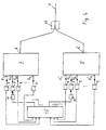
- the wavelength division multiplex transmission unit 1 shown in FIG. 1 comprises a wavelength monitoring and coupling unit 3 with n inputs E 1 , E 2 , E 3 to E n and an output A.
- the output A can be connected to an optical fiber 5 of a wavelength division multiplex transmission link .
- the inputs E 2 , E 4 to E n-1 are connected to optical transmission elements 7, which are, for. B. can be laser diodes.
- the remaining inputs E 1 , E 3 to E n are each connected to an optical receiving element 9.
- the optical transmission elements 7 are each cooled by means of a cooling element 11. For example, these can be Peltier elements.
- the output signals of the optical reception elements 9 are fed to an evaluation and control unit 13, which evaluate the signal of the optical reception elements 9. Depending on the result of the evaluation, the evaluation and control unit 13 can control the cooling elements 11 such that the center frequency of the transmission spectra of the optical transmission elements 7 is kept constant within predetermined limits.
- the optical wavelength monitoring and coupling unit 3 has the following properties: Between each of the inputs E 1 to E n and the common output A, an optical path is provided, in which narrow-band filtering with a central wavelength ⁇ 1 , ⁇ 2 ,. ⁇ 3 to ⁇ n takes place.
- the bandpass characteristics of the inputs E 1 , E 2 and E 3 are shown in FIG. 2, the transmission of the relevant optical path being drawn with t.
- the transmission spectrum 15 of the optical transmission element 7 connected to the input E 2 is shown in broken lines in FIG. The largest part of the transmission spectrum 15 is located within the characteristic of the optical path between the input E 2 and the output A.
- the lateral edge regions of the transmission spectrum 15 of the optical transmission element 7 extend into the bandpass characteristics between the input E 1 and the output A. or the input E 3 and the output A.
- the bandpass characteristics of the neighboring ones Inputs of the wavelength monitoring and coupling unit 3 preferably right next to each other. However, this is not absolutely necessary.
- the wavelength monitoring and coupling unit 3 has the property that those spectral components of a transmission spectrum applied to any input E i that are outside the bandpass characteristic between this input E; and the output A are present as an output signal at those inputs E j in whose bandpass characteristics (again between the respective input E j and the output A) the relevant spectral components fall.
- a shift of the transmission spectrum 15 in the direction of smaller wavelengths is determined by the evaluation and control unit 13 when the output signal of the receiving element 9 connected to the input E 1 reflects a higher power and the output signal of the receiving element connected to the input E 3 shows a lower power compared to the original condition.
- the wavelength and coupling unit 3 can in the simplest way by Use a phased array with an appropriate number of Inputs and an output can be realized. This results in a extremely low structural and thus financial expenditure.
- the wavelength and coupling unit 3 can also be used in other ways, for example using a Bragg grating or several Fabry-Perot filters being constructed.
- the second embodiment shown in FIG. 3 comprises instead of one Combined wavelength monitoring and coupling unit 3 of a separate Wavelength monitoring unit 30.
- This can basically be the same be constructed and have the same properties as above in Connection with Fig. 1 for the wavelength monitoring and coupling unit 30 described.
- the wavelength monitoring unit 30 does not have to also additionally summarizing the output signals of the transmission elements 7 take.
- the outputs of the transmission elements 7 emitting the transmission power are not connected to the inputs E 2 , E 4 ,... E n-1 , but rather a fraction of the power is decoupled separately from each transmission element 7 and the Monitoring unit 30 supplied in the manner already described.
- the optical power that occurs there is fed to the optical receiving elements coupled to it.
- the monitoring and control of the transmission elements 9 is carried out as described above.
- the combination of the transmission signals of the transmission elements 9 in one common output A can in this embodiment, for example done by a simple passive broadband m x 1 coupler 15, whereby m means the number of transmission elements. Of course it can Combining the transmission signals in turn to several common Outputs take place.
- the monitoring unit 30 constructed like that Wavelength monitoring and coupling unit 3, for example in the form of a commercially available phased array, output A of the monitoring unit 30 remain unused. However, it can also be used for further analysis of the multiplex transmission signal be used.
- Fig. 4 shows a wavelength division multiplex transmission unit in principle two Transmitter units according to FIG. 1 are cascaded. Instead of two evaluation and Control units 13 to reduce the effort, however, only one Evaluation and control unit 13 'used.
- the wavelength monitoring and coupling units 3, 3 ' are designed such that the center wavelength of each input E j ' of the unit 3 'matches the center wavelength of the input E j-1 of the unit 3 and the preferably constant distance between the individual channels (each input to Output with a certain spectral width ⁇ ) with respect to the center wavelength ⁇ j is the same for both wavelength monitoring and coupling units 3, 3 '.
- This has the advantage that an optimal utilization of the bandwidth can be guaranteed.
- the channels of the spectral width ⁇ can be directly adjacent, ie the distance between adjacent channels is chosen to be the same size as the spectral width of a channel.
- the inputs adjacent to each input for each wavelength monitoring and coupling unit 3, 3 'with coupled transmitter element 7 can be used for the wavelength monitoring of this transmitter element.
- the wavelength monitoring unit and the Combined wavelength monitoring and coupling unit can be constructed in any other way, as long as the basic principle is realized, at least the signal of a transmission element with at least one To apply high-pass, low-pass or bandpass characteristics that so is chosen that when the transmission spectrum is shifted by a small Amount a change in the power of the filtered (partial) signal takes place.
Landscapes
- Physics & Mathematics (AREA)
- Electromagnetism (AREA)
- Engineering & Computer Science (AREA)
- Computer Networks & Wireless Communication (AREA)
- Signal Processing (AREA)
- Optical Communication System (AREA)
- Spectrometry And Color Measurement (AREA)
- Semiconductor Lasers (AREA)
Description
- Fig. 1
- ein schematisches Blockdiagramm einer optischen Wellenlängenmultiplex- Sendeeinheit nach der Erfindung;
- Fig. 2
- ein Diagramm mit der spektralen Transmissions-Charakteristik t(λ) der Wellenlängenmultiplexeinheit der Wellenlängenmultiplex-Sendeeinheit in Fig. 1;
- Fig. 3
- ein schematisches Blockdiagramm einer zweiten Ausführungsform einer optischen Wellenlängenmultiplex- Sendeeinheit nach der Erfindung und
- Fig. 4
- ein schematisches Blockdiagramm einer dritten Ausführungsform einer optischen Wellenlängenmultiplex- Sendeeinheit nach der Erfindung.
Claims (12)
- Verfahren zur Erfassung und/oder Regelung der Sendewellenlängen von Sendeelementen einer optischen Wellenlängenmultiplex-Sendeeinheit,a) bei dem die Ausgangssignale mehrerer optischer Sendeelemente (7) mit jeweils einem optischen Sendespektrum (15) unterschiedlicher Mittenwellenlänge (λsj) jeweils einem optischen Eingang (E2, E4,..., En1) einer optischen Wellenlängenmonitoring- und Koppeleinheit (3) zugeführt werden, welche die Ausgangssignale an einem oder mehreren optischen Ausgängen (A) zu einem Wellenlängenmultiplexsignal zusammenführt,b) wobei die Wellenlängenmonitoring- und Koppeleinheit (3) so ausgebildet ist, dass zwischen einem, mehreren oder allen Eingängen (E2, E4,..., En-1), welchen das Ausgangssignal eines Sendeelements (7) zugeführt wird, und einem oder mehreren weiteren, nicht mit Sendeelementen (7) verbundenen Eingängen (E1, E3,..., En) ein optischer Pfad vorhanden ist, in dem eine schmalbandige, Hochpass- oder Tiefpassfilterung erfolgt,c) wobei die Filtercharakteristik in dem Pfad so gewählt wird, dass sich bei einer Verschiebung der Mittenwellenlänge des Sendespektrums (15) eines Sendeelements (7), dessen Signal in diesen Pfad gelangt, die gesamte spektrale Leistung des mit der gewählten Charakteristik gefilterten Signals verändert, undd) bei dem das an dem einen oder den mehreren weiteren Eingängen (E1, E3,..., En) auftretende gefilterte optische Signal jeweils einem optischen Empfangselement (9) zugeführt wird, dessen Ausgangssignal zur Erfassung der Lage und/oder zur Regelung der Lage des Sendespektrums (15) eines oder mehrerer der optischen Sendeelemente (7) ausgewertet wird.
- Verfahren zur Erfassung und/oder Regelung der Sendewellenlängen von Sendeelementen einer optischen Wellenlängenmultiplex-Sendeeinheit,a) bei dem die Ausgangssignale mehrerer optischer Sendeelemente (7) mit jeweils einem optischen Sendespektrum (15) unterschiedlicher Mittenwellenlänge (λsj) einer Koppeleinheit (17) zugeführt wird, welche die Sendepektren (15) der optischen Sendeelemente (7) an einem oder mehreren optischen Ausgängen (A) zusammenführt,b) bei dem ein geringer Bruchteil der Sendeleistung des Ausgangssignals eines oder mehrerer Sendeelemente (7) jeweils einem optischen Eingang (E2, E4,..., En1) einer optischen Wellenlängenmonitoring-Einheit (30) zugeführt wird,c) wobei die Wellenmonitoring-Einheit (30) so ausgebildet ist, dass zwischen einem, mehreren oder allen Eingängen (E2, E4,..., En-1), welchen der Bruchteil der Sendeleistung des Ausgangssignals eines Sendeelements (7) zugeführt wird, und einem oder mehreren weiteren, nicht mit Sendeelementen (7) verbundenen Eingängen (E1, E3,..., En) ein optischer Pfad vorhanden ist, in dem eine schmalbandige, Hochpass- oder Tiefpassfilterung erfolgt,d) wobei die Filtercharakteristik in dem Pfad so gewählt wird, dass sich bei einer Verschiebung der Mittenwellenlänge des Sendespektrums (15) eines Sendeelements (7), dessen Signal in diesen Pfad gelangt, die gesamte spektrale Leistung des mit der gewählten Charakteristik gefilterten Signals verändert, unde) bei dem das an dem einen oder den mehreren weiteren Eingängen (E1, E3,..., En) auftretende gefilterte optische Signal einem optischen Empfangselement (9) zugeführt wird, dessen Ausgangssignal zur Erfassung der Lage oder zur Regelung der Lage des Sendespektrums (15) eines oder mehrerer der optischen Sendeelemente (7) ausgewertet wird.
- Verfahren nach Anspruch 1 oder 2, dadurch gekennzeichnet, dass das Ausgangssignal des wenigstens einen optischen Empfangselements (9) hinsichtlich eines Überschreitens und/oder Unterschreitens jeweils eines vorbestimmbaren Schwellwerts überwacht wird und bei Detektieren eines Überschreitens oder Unterschreitens ein Fehlersignal erzeugt wird.
- Verfahren nach einem der vorhergehenden Ansprüche, dadurch gekennzeichnet, dass das Ausgangssignal des wenigstens einen optischen Empfangselements (9) zur Regelung eines die Mittenwellenlänge (λ2, λ4,..., λn-1) wenigstens eines optischen Sendeelements (7) beeinflussendenden Kenngröße verwendet wird.
- Optische Wellenlängenmultiplex-Sendeeinheita) mit mehreren optischen Sendeelementen (7) mit jeweils einem optischen Sendespektrum (15) unterschiedlicher Mittenwellenlänge (λ sj), deren Ausgangssignal jeweils einem optischen Eingang (E2, E4,..., En1) einer optischen Wellenlängenmonitoring- und Koppeleinheit (3) zugeführt ist, welche die Ausgangssignale an einem oder mehreren optischen Ausgängen (A) zu einem Wellenlängenmultiplexsignal zusammenführt,b) wobei die Wellenlängenmonitoring- und Koppeleinheit (3) so ausgebildet ist, dass zwischen einem, mehreren oder allen Eingängen (E2, E4,..., En-1), welchen das Ausgangssignal eines Sendeelements (7) zugeführt ist, und einem oder mehreren weiteren, nicht mit Sendeelementen (7) verbundenen Eingängen (E1, E3,..., En) ein optischer Pfad vorhanden ist, in dem eine schmalbandige, Hochpass- oder Tiefpassfilterung erfolgt,c) wobei die Filtercharakteristik in dem Pfad so gewählt ist, dass sich bei einer Verschiebung der Mittenwellenlänge des Sendespektrums (15) eines Sendeelements (7), dessen Signal in diesen Pfad gelangt, die gesamte spektrale Leistung des mit der gewählten Charakteristik gefilterten Signals verändert, undd) mit einem oder mehreren optischen Empfangselementen (9), welche jeweils mit einem der weiteren Eingänge (E1, E3,..., En) verbunden sind und welche das an diesen auftretende gefilterte optische Signal detektieren, unde) und mit einer Auswerte- und Steuereinheit (13), welcher das Ausgangssignal des wenigstens einen Empfangselements (9) zugeführt ist, und welche das Signal des Empfangselements (9) zur Erfassung der Lage und/oder zur Regelung der Lage des Sendespektrums (15) eines oder mehrerer der optischen Sendeelemente (7) auswertet.
- Optische Wellenlängenmultiplex-Sendeeinheita) mit mehreren optischen Sendeelementen (7) mit jeweils einem optischen Sendespektrum (15) unterschiedlicher Mittenwellenlänge (λ sj), deren Ausgangssignal jeweils einem optischen Eingang (E2, E4,..., En1) einer optischen Koppeleinheit (17) zugeführt ist, welche die Ausgangssignale an einem oder mehreren optischen Ausgängen (A) zu einem Wellenlängenmultiplexsignal zusammenführt,b) wobei ein geringer Bruchteil der Sendeleistung des Ausgangssignals eines oder mehrerer Sendeelemente (7) jeweils einem optischen Eingang (E2, E4,..., En1) einer optischen Wellenlängenmonitoring-Einheit (30) zugeführt ist, undc) wobei die Wellenmonitoring-Einheit (30) so ausgebildet ist, dass zwischen einem, mehreren oder allen Eingängen (E2, E4,..., En-1), welchen der Bruchteil der Sendeleistung des Ausgangssignals eines Sendeelements (7) zugeführt wird, und einem oder mehreren weiteren, nicht mit Sendeelementen (7) verbundenen Eingängen (E1, E3,..., En) ein optischer Pfad vorhanden ist, in dem eine schmalbandige, Hochpass- oder Tiefpassfilterung erfolgt,d) wobei die Filtercharakteristik in dem Pfad so gewählt wird, dass sich bei einer Verschiebung der Mittenwellenlänge des Sendespektrums (15) eines Sendeelements (7), dessen Signal in diesen Pfad gelangt, die gesamte spektrale Leistung des mit der gewählten Charakteristik gefilterten Signals verändert,e) mit einem oder mehreren optischen Empfangselementen (9), welche jeweils mit einem der weiteren Eingänge (E1, E3,..., En) verbunden sind und welche das an diesen auftretende gefilterte optische Signal detektieren, undf) mit einer Auswerte- und Steuereinheit (13), welcher das Ausgangssignal des wenigstens einen Empfangselements (9) zugeführt ist, und welche das Signal des Empfangselements (9) zur Erfassung der Lage und/oder zur Regelung der Lage des Sendespektrums (15) eines oder mehrerer der optischen Sendeelemente (7) auswertet.
- Optische Wellenlängenmultiplex-Sendeeinheit nach Anspruch 5 oder 6, dadurch gekennzeichnet, dass die Wellenlängenmonitoring- und Koppeleinheit (3) oder die Wellenlängenmonitoringeinheit (30) so ausgebildet sind, dass jedem Eingang eine schmalbandige Filtercharakteristik mit einer für jeden Eingang unterschiedlichen Mittenwellenlänge (λ1, λ2, ..., λn) zugeordnet ist und dass zwischen allen Eingängen (E1, E2,..., En) optische Pfade vorgesehen sind, in denen das darin geführte optische Signal zumindest mit derjenigen Filtercharakteristik gefiltert wird, die hinsichtlich des Signalwegs dem am Ende des optischen Pfads liegenden Eingang (E1, E2,..., En) zugeordnet ist.
- Optische Wellenlängenmultiplex-Sendeeinheit nach Anspruch 7, dadurch gekennzeichnet, dass die Wellenlängenmonitoring- und Koppeleinheit (3) oder die Wellenlängenmonitoringeinheit als Phased-Array ausgebildet oder unter Verwendung eines Bragg-Gitters realisiert ist.
- Optische Wellenlängenmultiplex-Sendeeinheit nach einem der Ansprüche 7 oder 8, dadurch gekennzeichnet, dass bezüglich der Mittenwellenlängen der (λ1, λ2, ..., λn) Filtercharakteristiken jeder zweite Eingang (E1, E3,..., En) der Wellenlängenmonitoring- und Koppeleinheit (3) oder der Wellenlängenmonitoringeinheit (3) mit einem optischen Empfangselement (7) und die übrigen Eingänge (E2, E4,..., En) den Ausgangssignalen eines optischen Sendeelements (7) beaufschlagt sind.
- Optische Wellenlängenmultiplex-Sendeeinheit nach Anspruch 9, dadurch gekennzeichnet, dass die Auswerte- und Steuereinheit (13) jedes Spektrum der Sendeelemente (7) durch Auswertung der Ausgangssignale zumindest beiden mit den benachbarten Eingängen verbundenen Empfangselemente erfasst und/oder hinsichtlich der Mittenwellenlänge regelt.
- Optische Wellenlängenmultiplex-Sendeeinheit nach Anspruch 9 oder 10, dadurch gekennzeichnet, dass zwei Wellenlängenmonitoring- und Koppeleinheiten (3) vorgesehen sind, wobei die den Eingängen (E1, E2,..., En) zugeordneten Filtercharakteristika hinsichtlich der Mittenwellenlänge im Wesentlichen um einen Eingang gegeneinander versetzt sind und dass die Ausgangssignale der zwei Wellenlängenmonitoring- und Koppeleinheiten (3) mittels einer Koppeleinheit (19) zu einem Gesamt-Wellenlängenmultiplexsignal zusammengefasst sind.
- Optische Wellenlängenmultiplex-Sendeeinheit nach Anspruch 9 oder 10, dadurch gekennzeichnet, dass zwei Wellenlängenmonitoringeinheiten (30) vorgesehen sind, wobei die den Eingängen (E1, E2,..., En) zugeordneten Filtercharakteristika hinsichtlich der Mittenwellenlänge im Wesentlichen um einen Eingang gegeneinander versetzt sind und dass die Ausgangssignale der zwei Wellenlängenmonitoringeinheiten (30) mittels einer gemeinsamen Koppeleinheit (17) zu einem Gesamt-Wellenlängenmultiplexsignal zusammengefasst sind.
Applications Claiming Priority (3)
| Application Number | Priority Date | Filing Date | Title |
|---|---|---|---|
| DE19828615A DE19828615A1 (de) | 1998-06-26 | 1998-06-26 | Verfahren zur Erfassung und/oder Regelung der Sendewellenlängen von Sendeelementen einer optischen Wellenlängenmultiplex--Sendeeinheit und entsprechende Wellenlängenmultiplex-Sendeeinheit |
| DE19828615 | 1998-06-26 | ||
| PCT/DE1999/001866 WO2000001106A1 (de) | 1998-06-26 | 1999-06-25 | Verfahren zur erfassung und/oder regelung der sendewellenlängen von sendeelementen einer optischen wellenlängenmultiplex-sendeeinheit und entsprechende wellenlängenmultiplex-sendeeinheit |
Publications (2)
| Publication Number | Publication Date |
|---|---|
| EP1090472A1 EP1090472A1 (de) | 2001-04-11 |
| EP1090472B1 true EP1090472B1 (de) | 2002-04-03 |
Family
ID=7872171
Family Applications (1)
| Application Number | Title | Priority Date | Filing Date |
|---|---|---|---|
| EP99939954A Expired - Lifetime EP1090472B1 (de) | 1998-06-26 | 1999-06-25 | Verfahren zur erfassung und/oder regelung der sendewellenlängen von sendeelementen einer optischen wellenlängenmultiplex-sendeeinheit und entsprechende wellenlängenmultiplex-sendeeinheit |
Country Status (6)
| Country | Link |
|---|---|
| US (1) | US6925266B1 (de) |
| EP (1) | EP1090472B1 (de) |
| JP (1) | JP2002519870A (de) |
| AT (1) | ATE215761T1 (de) |
| DE (2) | DE19828615A1 (de) |
| WO (1) | WO2000001106A1 (de) |
Families Citing this family (4)
| Publication number | Priority date | Publication date | Assignee | Title |
|---|---|---|---|---|
| KR100498954B1 (ko) * | 2003-08-27 | 2005-07-04 | 삼성전자주식회사 | 루프-백 광원을 이용한 파장분할다중방식 수동형 광가입자망의 광 파장 트래킹 장치 및 방법 |
| US7881612B2 (en) * | 2005-06-30 | 2011-02-01 | Infinera Corporation | Optical autodiscovery for automated logical and physical connectivity check between optical modules |
| JP4892262B2 (ja) | 2006-03-23 | 2012-03-07 | 富士通株式会社 | 光源波長制御装置 |
| JP6498479B2 (ja) * | 2015-03-10 | 2019-04-10 | 日置電機株式会社 | 光量測定装置 |
Family Cites Families (6)
| Publication number | Priority date | Publication date | Assignee | Title |
|---|---|---|---|---|
| JPH0879218A (ja) * | 1994-08-31 | 1996-03-22 | Canon Inc | 波長可変フィルタ制御方式及びそれを用いた光通信システム |
| JPH0879128A (ja) | 1994-09-02 | 1996-03-22 | Canon Inc | スペクトラム拡散無線通信システム |
| KR970008300B1 (en) * | 1994-12-02 | 1997-05-22 | Korea Electronics Telecomm | Locking apparatus for multiplexing optic frequencies |
| JPH08293853A (ja) | 1995-04-24 | 1996-11-05 | Hitachi Ltd | 波長制御方法 |
| US6304350B1 (en) * | 1997-05-27 | 2001-10-16 | Lucent Technologies Inc | Temperature compensated multi-channel, wavelength-division-multiplexed passive optical network |
| US6301031B2 (en) * | 1997-09-02 | 2001-10-09 | Agere Systems Optoelectronics Guardian Corp. | Method and apparatus for wavelength-channel tracking and alignment within an optical communications system |
-
1998
- 1998-06-26 DE DE19828615A patent/DE19828615A1/de not_active Withdrawn
-
1999
- 1999-06-25 US US09/720,599 patent/US6925266B1/en not_active Expired - Fee Related
- 1999-06-25 JP JP2000557577A patent/JP2002519870A/ja not_active Withdrawn
- 1999-06-25 WO PCT/DE1999/001866 patent/WO2000001106A1/de not_active Ceased
- 1999-06-25 EP EP99939954A patent/EP1090472B1/de not_active Expired - Lifetime
- 1999-06-25 DE DE59901133T patent/DE59901133D1/de not_active Expired - Lifetime
- 1999-06-25 AT AT99939954T patent/ATE215761T1/de not_active IP Right Cessation
Also Published As
| Publication number | Publication date |
|---|---|
| EP1090472A1 (de) | 2001-04-11 |
| DE59901133D1 (de) | 2002-05-08 |
| WO2000001106A1 (de) | 2000-01-06 |
| ATE215761T1 (de) | 2002-04-15 |
| US6925266B1 (en) | 2005-08-02 |
| JP2002519870A (ja) | 2002-07-02 |
| DE19828615A1 (de) | 1999-12-30 |
Similar Documents
| Publication | Publication Date | Title |
|---|---|---|
| DE69826104T2 (de) | Frequenznachlauf in abstimmbaren optischen Systemen | |
| EP0970550B1 (de) | Lasermodul mit wellenlängenstabilisierung | |
| EP0284908B1 (de) | Anordnung zur Steuerung oder Regelung einer Emissionswellenlänge und emittierten Leistung eines Halbleiterlasers | |
| DE69013662T2 (de) | Schmalbandige Laserquelle. | |
| DE68920047T2 (de) | Geräuschmessung für eine faseroptische verbindung und optimierungssystem. | |
| DE69627438T9 (de) | Verfahren und Vorrichtung zum Niveauausgleich der Leistung der Kanäle eines spektral gemultiplexten optischen Signals | |
| DE69311048T2 (de) | Multi/Demultiplexer mit Gitter aus gruppierten Wellenleitern und zurückgefürten optischen Wegen | |
| DE19734957C1 (de) | Verfahren und Anordnung zur Wellenlängenstabilisierung für mehrkanalige optische Übertragungssysteme | |
| DE60204542T2 (de) | Verschachtler und Entschachtler | |
| DE69628486T2 (de) | Wellenlängenzuordnung in einem optischen Übertragungssystem | |
| DE60220668T2 (de) | Verfahren zur adaptiven Rückkopplungssteuerung der Farbzerstreuungskompensation | |
| EP0130223B1 (de) | Symmetrischer Wellenleiter-Koppler | |
| EP1090472B1 (de) | Verfahren zur erfassung und/oder regelung der sendewellenlängen von sendeelementen einer optischen wellenlängenmultiplex-sendeeinheit und entsprechende wellenlängenmultiplex-sendeeinheit | |
| DE69633843T2 (de) | Verfahren und Vorrichtung zur optischen Übertragung anhand einer Vielzahl von Wellenlängen | |
| DE69533348T2 (de) | Kontrolle der Wellenlänge in einem WDM-System | |
| DE69323379T2 (de) | Faseroptisches Kommunikationsendgerät, faseroptisches Übertragungssystem und Verfahren zur Einstellung der Wellenlänge | |
| EP1588511B1 (de) | Ausgangsstufe fur die wdm-nachrichtenubertragung und verfahren zum austauschen von fullichtquellen in einer solchen ausgangsstufe | |
| EP0786879A2 (de) | Verfahren und Schaltungs-Anordnung zur Frequenz-Stabilisierung eines WDM-Multiplexers/-Demultiplexers | |
| EP0522379A2 (de) | Optisches Zeitmultiplexen | |
| EP2940911B1 (de) | Optisches Übertragungsnetzwerk und optische Netzelemente zum Übertragen von WDM-Signalen | |
| DE10046585B4 (de) | Modular erweiterbares optisches ADD-DROP-Modul | |
| EP0786677B1 (de) | Verfahren zum Betrieb eines Phased Array | |
| DE69907819T2 (de) | Verfahren und Vorrichtung zur Regeneration und Zwischenverstärkung eines optischen Übertragungssignals und Wellenlängenmultiplexübertragungssystem das diese verwendet | |
| EP3330684B1 (de) | Verfahren zum sicherstellen eines modulationsbereichs | |
| DE69231884T2 (de) | Integriert optischer Nahfeldkoppler |
Legal Events
| Date | Code | Title | Description |
|---|---|---|---|
| PUAI | Public reference made under article 153(3) epc to a published international application that has entered the european phase |
Free format text: ORIGINAL CODE: 0009012 |
|
| 17P | Request for examination filed |
Effective date: 20001221 |
|
| AK | Designated contracting states |
Kind code of ref document: A1 Designated state(s): AT BE CH CY DE DK ES FI FR GB GR IE IT LI LU MC NL PT SE |
|
| RAP3 | Party data changed (applicant data changed or rights of an application transferred) |
Owner name: AIFOTEC GMBH |
|
| GRAG | Despatch of communication of intention to grant |
Free format text: ORIGINAL CODE: EPIDOS AGRA |
|
| 17Q | First examination report despatched |
Effective date: 20010611 |
|
| GRAG | Despatch of communication of intention to grant |
Free format text: ORIGINAL CODE: EPIDOS AGRA |
|
| GRAH | Despatch of communication of intention to grant a patent |
Free format text: ORIGINAL CODE: EPIDOS IGRA |
|
| REG | Reference to a national code |
Ref country code: GB Ref legal event code: IF02 |
|
| GRAH | Despatch of communication of intention to grant a patent |
Free format text: ORIGINAL CODE: EPIDOS IGRA |
|
| GRAA | (expected) grant |
Free format text: ORIGINAL CODE: 0009210 |
|
| AK | Designated contracting states |
Kind code of ref document: B1 Designated state(s): AT BE CH CY DE DK ES FI FR GB GR IE IT LI LU MC NL PT SE |
|
| PG25 | Lapsed in a contracting state [announced via postgrant information from national office to epo] |
Ref country code: NL Free format text: LAPSE BECAUSE OF FAILURE TO SUBMIT A TRANSLATION OF THE DESCRIPTION OR TO PAY THE FEE WITHIN THE PRESCRIBED TIME-LIMIT Effective date: 20020403 Ref country code: IE Free format text: LAPSE BECAUSE OF FAILURE TO SUBMIT A TRANSLATION OF THE DESCRIPTION OR TO PAY THE FEE WITHIN THE PRESCRIBED TIME-LIMIT Effective date: 20020403 Ref country code: GR Free format text: LAPSE BECAUSE OF FAILURE TO SUBMIT A TRANSLATION OF THE DESCRIPTION OR TO PAY THE FEE WITHIN THE PRESCRIBED TIME-LIMIT Effective date: 20020403 Ref country code: FI Free format text: LAPSE BECAUSE OF FAILURE TO SUBMIT A TRANSLATION OF THE DESCRIPTION OR TO PAY THE FEE WITHIN THE PRESCRIBED TIME-LIMIT Effective date: 20020403 |
|
| REF | Corresponds to: |
Ref document number: 215761 Country of ref document: AT Date of ref document: 20020415 Kind code of ref document: T |
|
| REG | Reference to a national code |
Ref country code: CH Ref legal event code: EP |
|
| REF | Corresponds to: |
Ref document number: 59901133 Country of ref document: DE Date of ref document: 20020508 |
|
| REG | Reference to a national code |
Ref country code: IE Ref legal event code: FG4D Free format text: GERMAN |
|
| RAP2 | Party data changed (patent owner data changed or rights of a patent transferred) |
Owner name: FINISAR EUROPE GMBH |
|
| PG25 | Lapsed in a contracting state [announced via postgrant information from national office to epo] |
Ref country code: MC Free format text: LAPSE BECAUSE OF NON-PAYMENT OF DUE FEES Effective date: 20020625 Ref country code: LU Free format text: LAPSE BECAUSE OF NON-PAYMENT OF DUE FEES Effective date: 20020625 Ref country code: AT Free format text: LAPSE BECAUSE OF NON-PAYMENT OF DUE FEES Effective date: 20020625 |
|
| PG25 | Lapsed in a contracting state [announced via postgrant information from national office to epo] |
Ref country code: CY Free format text: LAPSE BECAUSE OF FAILURE TO SUBMIT A TRANSLATION OF THE DESCRIPTION OR TO PAY THE FEE WITHIN THE PRESCRIBED TIME-LIMIT Effective date: 20020630 Ref country code: BE Free format text: LAPSE BECAUSE OF NON-PAYMENT OF DUE FEES Effective date: 20020630 |
|
| PG25 | Lapsed in a contracting state [announced via postgrant information from national office to epo] |
Ref country code: SE Free format text: LAPSE BECAUSE OF FAILURE TO SUBMIT A TRANSLATION OF THE DESCRIPTION OR TO PAY THE FEE WITHIN THE PRESCRIBED TIME-LIMIT Effective date: 20020703 Ref country code: PT Free format text: LAPSE BECAUSE OF FAILURE TO SUBMIT A TRANSLATION OF THE DESCRIPTION OR TO PAY THE FEE WITHIN THE PRESCRIBED TIME-LIMIT Effective date: 20020703 Ref country code: DK Free format text: LAPSE BECAUSE OF FAILURE TO SUBMIT A TRANSLATION OF THE DESCRIPTION OR TO PAY THE FEE WITHIN THE PRESCRIBED TIME-LIMIT Effective date: 20020703 |
|
| NLT2 | Nl: modifications (of names), taken from the european patent patent bulletin |
Owner name: FINISAR EUROPE GMBH |
|
| GBT | Gb: translation of ep patent filed (gb section 77(6)(a)/1977) |
Effective date: 20020729 |
|
| NLV1 | Nl: lapsed or annulled due to failure to fulfill the requirements of art. 29p and 29m of the patents act | ||
| ET | Fr: translation filed | ||
| PG25 | Lapsed in a contracting state [announced via postgrant information from national office to epo] |
Ref country code: ES Free format text: LAPSE BECAUSE OF FAILURE TO SUBMIT A TRANSLATION OF THE DESCRIPTION OR TO PAY THE FEE WITHIN THE PRESCRIBED TIME-LIMIT Effective date: 20021030 |
|
| REG | Reference to a national code |
Ref country code: IE Ref legal event code: FD4D Ref document number: 1090472E Country of ref document: IE Ref country code: GB Ref legal event code: 732E |
|
| BERE | Be: lapsed |
Owner name: *AIFOTEC G.M.B.H. Effective date: 20020630 |
|
| PLBE | No opposition filed within time limit |
Free format text: ORIGINAL CODE: 0009261 |
|
| STAA | Information on the status of an ep patent application or granted ep patent |
Free format text: STATUS: NO OPPOSITION FILED WITHIN TIME LIMIT |
|
| 26N | No opposition filed |
Effective date: 20030106 |
|
| PG25 | Lapsed in a contracting state [announced via postgrant information from national office to epo] |
Ref country code: LI Free format text: LAPSE BECAUSE OF NON-PAYMENT OF DUE FEES Effective date: 20030630 Ref country code: CH Free format text: LAPSE BECAUSE OF NON-PAYMENT OF DUE FEES Effective date: 20030630 |
|
| REG | Reference to a national code |
Ref country code: GB Ref legal event code: 732E |
|
| REG | Reference to a national code |
Ref country code: CH Ref legal event code: PL |
|
| REG | Reference to a national code |
Ref country code: FR Ref legal event code: TP |
|
| PG25 | Lapsed in a contracting state [announced via postgrant information from national office to epo] |
Ref country code: IT Free format text: LAPSE BECAUSE OF NON-PAYMENT OF DUE FEES Effective date: 20100625 |
|
| PGFP | Annual fee paid to national office [announced via postgrant information from national office to epo] |
Ref country code: GB Payment date: 20140627 Year of fee payment: 16 |
|
| PGFP | Annual fee paid to national office [announced via postgrant information from national office to epo] |
Ref country code: IT Payment date: 20140625 Year of fee payment: 16 |
|
| PGFP | Annual fee paid to national office [announced via postgrant information from national office to epo] |
Ref country code: DE Payment date: 20140627 Year of fee payment: 16 |
|
| PGFP | Annual fee paid to national office [announced via postgrant information from national office to epo] |
Ref country code: FR Payment date: 20140617 Year of fee payment: 16 |
|
| REG | Reference to a national code |
Ref country code: DE Ref legal event code: R119 Ref document number: 59901133 Country of ref document: DE |
|
| PG25 | Lapsed in a contracting state [announced via postgrant information from national office to epo] |
Ref country code: IT Free format text: LAPSE BECAUSE OF NON-PAYMENT OF DUE FEES Effective date: 20150625 |
|
| GBPC | Gb: european patent ceased through non-payment of renewal fee |
Effective date: 20150625 |
|
| REG | Reference to a national code |
Ref country code: FR Ref legal event code: ST Effective date: 20160229 |
|
| PG25 | Lapsed in a contracting state [announced via postgrant information from national office to epo] |
Ref country code: GB Free format text: LAPSE BECAUSE OF NON-PAYMENT OF DUE FEES Effective date: 20150625 Ref country code: DE Free format text: LAPSE BECAUSE OF NON-PAYMENT OF DUE FEES Effective date: 20160101 |
|
| PG25 | Lapsed in a contracting state [announced via postgrant information from national office to epo] |
Ref country code: FR Free format text: LAPSE BECAUSE OF NON-PAYMENT OF DUE FEES Effective date: 20150630 |