EP1090168B1 - Electrical resistance heater for crystal growing apparatus and its method of use - Google Patents
Electrical resistance heater for crystal growing apparatus and its method of use Download PDFInfo
- Publication number
- EP1090168B1 EP1090168B1 EP99930636A EP99930636A EP1090168B1 EP 1090168 B1 EP1090168 B1 EP 1090168B1 EP 99930636 A EP99930636 A EP 99930636A EP 99930636 A EP99930636 A EP 99930636A EP 1090168 B1 EP1090168 B1 EP 1090168B1
- Authority
- EP
- European Patent Office
- Prior art keywords
- heating element
- ingot
- housing
- molten silicon
- growing
- Prior art date
- Legal status (The legal status is an assumption and is not a legal conclusion. Google has not performed a legal analysis and makes no representation as to the accuracy of the status listed.)
- Expired - Lifetime
Links
Images


Classifications
-
- C—CHEMISTRY; METALLURGY
- C30—CRYSTAL GROWTH
- C30B—SINGLE-CRYSTAL GROWTH; UNIDIRECTIONAL SOLIDIFICATION OF EUTECTIC MATERIAL OR UNIDIRECTIONAL DEMIXING OF EUTECTOID MATERIAL; REFINING BY ZONE-MELTING OF MATERIAL; PRODUCTION OF A HOMOGENEOUS POLYCRYSTALLINE MATERIAL WITH DEFINED STRUCTURE; SINGLE CRYSTALS OR HOMOGENEOUS POLYCRYSTALLINE MATERIAL WITH DEFINED STRUCTURE; AFTER-TREATMENT OF SINGLE CRYSTALS OR A HOMOGENEOUS POLYCRYSTALLINE MATERIAL WITH DEFINED STRUCTURE; APPARATUS THEREFOR
- C30B29/00—Single crystals or homogeneous polycrystalline material with defined structure characterised by the material or by their shape
- C30B29/02—Elements
- C30B29/06—Silicon
-
- C—CHEMISTRY; METALLURGY
- C30—CRYSTAL GROWTH
- C30B—SINGLE-CRYSTAL GROWTH; UNIDIRECTIONAL SOLIDIFICATION OF EUTECTIC MATERIAL OR UNIDIRECTIONAL DEMIXING OF EUTECTOID MATERIAL; REFINING BY ZONE-MELTING OF MATERIAL; PRODUCTION OF A HOMOGENEOUS POLYCRYSTALLINE MATERIAL WITH DEFINED STRUCTURE; SINGLE CRYSTALS OR HOMOGENEOUS POLYCRYSTALLINE MATERIAL WITH DEFINED STRUCTURE; AFTER-TREATMENT OF SINGLE CRYSTALS OR A HOMOGENEOUS POLYCRYSTALLINE MATERIAL WITH DEFINED STRUCTURE; APPARATUS THEREFOR
- C30B15/00—Single-crystal growth by pulling from a melt, e.g. Czochralski method
- C30B15/14—Heating of the melt or the crystallised materials
-
- C—CHEMISTRY; METALLURGY
- C30—CRYSTAL GROWTH
- C30B—SINGLE-CRYSTAL GROWTH; UNIDIRECTIONAL SOLIDIFICATION OF EUTECTIC MATERIAL OR UNIDIRECTIONAL DEMIXING OF EUTECTOID MATERIAL; REFINING BY ZONE-MELTING OF MATERIAL; PRODUCTION OF A HOMOGENEOUS POLYCRYSTALLINE MATERIAL WITH DEFINED STRUCTURE; SINGLE CRYSTALS OR HOMOGENEOUS POLYCRYSTALLINE MATERIAL WITH DEFINED STRUCTURE; AFTER-TREATMENT OF SINGLE CRYSTALS OR A HOMOGENEOUS POLYCRYSTALLINE MATERIAL WITH DEFINED STRUCTURE; APPARATUS THEREFOR
- C30B15/00—Single-crystal growth by pulling from a melt, e.g. Czochralski method
- C30B15/20—Controlling or regulating
- C30B15/206—Controlling or regulating the thermal history of growing the ingot
-
- Y—GENERAL TAGGING OF NEW TECHNOLOGICAL DEVELOPMENTS; GENERAL TAGGING OF CROSS-SECTIONAL TECHNOLOGIES SPANNING OVER SEVERAL SECTIONS OF THE IPC; TECHNICAL SUBJECTS COVERED BY FORMER USPC CROSS-REFERENCE ART COLLECTIONS [XRACs] AND DIGESTS
- Y10—TECHNICAL SUBJECTS COVERED BY FORMER USPC
- Y10T—TECHNICAL SUBJECTS COVERED BY FORMER US CLASSIFICATION
- Y10T117/00—Single-crystal, oriented-crystal, and epitaxy growth processes; non-coating apparatus therefor
- Y10T117/10—Apparatus
- Y10T117/1016—Apparatus with means for treating single-crystal [e.g., heat treating]
Definitions
- the present invention relates generally to crystal growing apparatus used in growing monocrystalline ingots, and more particularly to an electrical resistance heater for use in such a crystal growing apparatus.
- Single crystal silicon which is the starting material for most semiconductor electronic component fabrication, is commonly prepared by the so-called Czochralski ("Cz") method.
- Cz Czochralski
- the growth of the crystal is most commonly carried out in a crystal pulling furnace.
- polycrystalline silicon (“polysilicon”) is charged to a crucible and melted by a heater surrounding the outer surface of the crucible side wall.
- a seed crystal is brought into contact with the molten silicon and a single crystal ingot is grown by slow extraction via a crystal puller. After formation of a neck is complete, the diameter of the crystal ingot is enlarged by decreasing the pulling rate and/or the melt temperature until the desired or target diameter is reached.
- the cylindrical main body of the crystal which has an approximately constant diameter is then grown by controlling the pull rate and the melt temperature while compensating for the decreasing melt level. Near the end of the growth process, the crystal diameter must be reduced gradually to form an end-cone. Typically, the end-cone is formed by increasing the pull rate and heat supplied to the crucible. When the diameter becomes small enough, the ingot is then separated from the melt.
- Heaters used for melting source material (e.g. silicon) in the crucible are typically electrical resistance heaters in which an electrical current flows through a heating element constructed of a resistive heating material (e.g., graphite). The resistance to the flow of current generates heat that radiates from the heating element to the crucible and silicon contained therein.
- the heating element comprises vertically oriented heating segments of equal length and cross-section arranged in side-by-side relationship and connected to each other in a serpentine configuration. That is, adjacent segments are connected to each other at the tops or bottoms of the segments in an alternating manner to form a continuous electrical circuit throughout the heating element.
- the heating power generated by the heating element is generally a function of the cross-sectional area of the segments.
- GOI Gate Oxide Integrity
- Silicon wafers sliced from the ingot and manufactured according to conventional processes often include a silicon oxide layer formed on the surface of the wafer. Electronic circuit devices such as MOS devices are fabricated on this silicon oxide layer. Defects in the surface of the wafer, caused by the agglomerations present in the growing crystal, lead to poor growth of the oxide layer. The quality of the oxide layer, often referred to as the oxide film dielectric breakdown strength, may be quantitatively measured by fabricating MOS devices on the oxide layer and testing the devices.
- the Gate Oxide Integrity (GOI) of the crystal is the percentage of operational devices on the oxide layer of the wafers processed from the crystal.
- the GOI of crystals grown by the Czochralski method can be improved by increasing the amount of time a growing ingot dwells in the temperature range above 1000°C, and more particularly in the range of 1150°C-1000°C. If the ingot cools too quickly through this temperature range, the vacancies will not have sufficient time to agglomerate together, resulting in a large number of small agglomerations within the ingot. This undesirably leads to a large number of small pits spread over the surfaces of the wafer, thereby negatively affecting GOI.
- Defects relating to self-interstitials are less well studied. They are generally regarded as being low densities of interstitial-type dislocation loops or networks. Such defects are not responsible for GOI failures, but they are widely recognized as the cause of other types of device failures usually associated with current leakage problems. It has been determined that the agglomeration of self-interstitials are undesirable and can be controlled by increasing the amount of time a growing ingot dwells in the temperature range above 1000°C. As portions of the ingot remain at temperatures above 1000°C for relatively long time durations, radial out-diffusion of self-interstitials from the ingot occurs to suppress the concentration below the critical concentration required for agglomeration of interstitial defects.
- U.S. Patent No. 5,248,378 discloses an apparatus for producing single silicon crystal in which a passive heat insulator is disposed in the crystal puller above the crucible to reduce the rate of cooling of the growing ingot above 1150°C.
- heat insulators or heat shields such as that disclosed by Oda et al. generally cannot slow the cooling of the ingot to a rate sufficient to substantially improve the GOI of the crystal or suppress the agglomeration of interstitial defects.
- Oda et al. further disclose that the insulator may be replaced by a heater for heating the growing ingot. While a heater similar to the conventional crucible heater described above would more actively apply heat to the ingot to reduce the cooling rate, using such a heater has a number of disadvantages.
- the heating power output of the conventional heater is generally constant along the height of the heater. A crystal ingot being pulled upward through the heater would be rapidly heated at the bottom of the heater to reduce the cooling of the ingot. The cooling rate would continue to decrease as the ingot passed upward through the heater and then increase upon reaching the top of the heater. For example, a plot of the axial temperature gradient of the ingot versus the ingot temperature would look similar to that shown in Fig.
- JP-A-05043385 discloses another conventional heater sized and shaped for being placed in a crystal puller surrounding the crucible for heating the crucible to melt silicon contained in the crucible.
- the heater has a cylindrical shape, with heater segments electrically connected together and all having the same length. Through holes positioned on each heater segment below the top of the heater increase the heating power output at the hole locations by decreasing the cross-sectional area (and thus increasing electrical resistance) of each heater segment at the hole locations.
- an electrical resistance heater for use in a crystal puller which facilitates the growth of crystals having an improved Gate Oxide Integrity; the provision of such a heater which provides a more uniform axial temperature gradient in the range of 1100°C-1000°C; the provision of such a heater which increases the dwell time of the ingot at a temperature above 1000°C; the provision of such a heater which increases the dwell time of the ingot temperature in the range of 1100°C to 1000°C; and the provision of such a heater which facilitates reduction of agglomeration of intrinsic point defects.
- an electrical resistance heater of the present invention is for use in a crystal puller used for growing monocrystalline silicon ingots according to the Czochralski method.
- a crystal puller has a housing, a crucible in the housing for containing molten silicon and a pulling mechanism for pulling a growing ingot upward from the molten silicon.
- the heater comprises a heating element sized and shaped for placement in the housing of the crystal puller generally above the crucible in spaced relationship with the outer surface of the growing ingot for radiating heat to the ingot as it is pulled upward in the housing relative to the molten silicon.
- the heating element has an upper end and a lower end.
- the lower end of the heating element is disposed substantially closer to the molten silicon than the upper end when the heating element is placed in the housing.
- the heating element is constructed such that the heating power output generated by the heating element gradually increases from the lower end to the upper end of the heating element.
- the heating element includes first and second vertically oriented heating segments arranged in a generally side-by-side relationship and being electrically connected together. The segments each have an upper end and a lower end, with the second segment having a length substantially greater than the first segment and being arranged so that when the heating element is placed in the housing the lower end of the second segment is disposed closer to the molten silicon in the crucible than the lower end of the first segment.
- a method of controlling the uniformity of the axial temperature gradient of a monocrystalline silicon ingot grown in a crystal puller used for growing monocrystalline silicon ingots according to the Czochralski method comprises allowing the ingot to cool to a predetermined first temperature as it is pulled upward in the housing from the molten silicon. Heat is radiated to the ingot as it is pulled further upward in the housing to reduce the cooling rate of the ingot as it cools down from the first temperature. The amount of heat radiated to the ingot is gradually increased as the ingot is pulled further upward in the housing to maintain a generally uniform axial temperature gradient of the ingot as the temperature of the ingot decreases from the first temperature down to a predetermined second temperature.
- the steps of radiating heat to the growing ingot and gradually increasing the heat radiated to the growing ingot as it is pulled further upward in the housing comprise pulling the growing ingot upward past an electrical resistance heater disposed in the housing generally above the crucible.
- the heater is constructed to generate a gradually increasing amount of heating power output as the ingot passes upward past the heater to reduce the axial temperature gradient of the ingot and increase the uniformity of the temperature gradient.
- the invention also provides a crystal puller for growing monocrystalline silicon ingots according to the Czochralski method, the crystal puller comprising a housing, a crucible in the housing for containing molten silicon, a pulling mechanism for pulling a growing ingot upward from the molten silicon, and an electrical resistance heater.
- the electrical resistance heater comprises a heating element sized and shaped for placement in the housing of the crystal puller generally above the crucible in spaced relationship with the outer surface of the growing ingot for radiating heat to the ingot as it is pulled upward in the housing relative to the molten silicon.
- the heating element has an upper end and a lower end. The lower end of the heating element is disposed substantially closer to the molten silicon than the upper end when the heating element is placed in the housing.
- the heating element is constructed such that the heating power output generated by the heating element gradually increases from the lower end to the upper end of the heating element. Moreover the heating element is sized and shaped to extend around at least a portion of the circumference of the crystal ingot when placed in the crystal puller, while the upper end of the heating element is sized and shaped to surround a substantially greater extent of the circumference of the ingot than the lower end of the heating element.
- the invention provides a crystal puller for growing monocrystalline silicon ingots according to the Czochralski method, the crystal puller comprising a housing, a crucible in the housing for containing molten silicon, a pulling mechanism for pulling a growing ingot upward from the molten silicon, and an electrical resistance heater.
- the electrical heater comprises a heating element sized and shaped for placement in the housing of the crystal puller generally above the crucible in spaced relationship with the outer surface of the growing ingot for radiating heat to the ingot as it is pulled upward in the housing relative to the molten silicon.
- the heating element has an upper end and a lower end, with the lower end of the heating element being disposed substantially closer to the molten silicon than the upper end when the heating element is placed in the housing.
- the heating element is constructed such that the heating power output generated by the heating element gradually increases from the lower end to the upper end of the heating element.
- the heating element includes first and second vertically oriented heating segments arranged in a generally side-by-side relationship and being electrically connected together.
- the segments each have an upper end and a lower end, with the second segment having a length substantially greater than the first segment and being arranged relative to the first segment so that when the heating element is placed in the housing the lower end of the second segment is disposed closer to the molten silicon in the crucible than the lower end of the first segment.
- the invention provides an electrical resistance heater for use in a crystal puller used for growing monocrystalline silicon ingots according to the Czochralski method.
- a crystal puller has a housing, a crucible in the housing for containing molten silicon and a pulling mechanism for pulling a growing ingot upward from the molten silicon.
- the heater comprises a heating element sized and shaped for placement in the housing of the crystal puller generally above the crucible in spaced relationship with the outer surface of the growing ingot for radiating heat to the ingot as it is pulled upward in the housing relative to the molten silicon.
- the heating element has an upper end and a lower end, with the lower end of the heating element being disposed substantially closer to the molten silicon than the upper end when the heating element is placed in the housing.
- the heating element is constructed such that the heating power output generated by the heating element gradually increases from the lower end to the upper end of the heating element.
- the heating element is sized and shaped to extend around at least a portion of the circumference of the crystal ingot when placed in the crystal puller.
- the upper end of the heating element has a greater circumferential extent than the lower end thereof to surround a substantially greater extent of the circumference of the ingot than the lower end of the heating element.
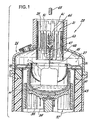
- an electrical resistance heater constructed according to the principles of the present invention is generally indicated at 21.
- the heater is preferably for use in a crystal puller, indicated generally at 23, of the type used to grow monocrystalline silicon ingots (e.g., ingot I of Fig. 1) according to the Czochralski method.
- the crystal puller 23 includes a housing (generally indicated at 25) for isolating an interior which includes a lower crystal growth chamber 27 and an upper pull chamber 29.
- the pull chamber 29 has a smaller transverse dimension than the growth chamber.
- a quartz crucible 31 contains molten semiconductor source material M from which the monocrystalline silicon ingot I is grown.
- the crucible 31 includes a cylindrical side wall 33 and is mounted on a turntable 35 for rotation about a vertical axis.
- the crucible 31 is also capable of being raised within the growth chamber 27 to maintain the surface of the molten source material M at the same level as the ingot I is grown and source material is removed from the melt.
- a crucible heater, generally indicated at 37, for melting the source material M in the crucible 31 includes a generally vertically oriented heating element 39 surrounding the crucible in radially spaced relationship with the side wall 33 of the crucible.
- the heating element 39 heats the crucible 31 and the interior of the crystal puller housing 25 to temperatures above the melting point of the source material M (e.g., silicon).
- Insulation 41 is positioned to confine the heat to the interior of the housing 25.
- a pulling mechanism includes a pull shaft 45 extending down from a mechanism (not shown) above the pull chamber 29 capable of raising, lowering and rotating the pull shaft.
- the crystal puller 23 may have a pull wire (not shown) rather than a shaft 45, depending upon the type of puller.
- the pull shaft 45 terminates in a seed crystal chuck 47 which holds a seed crystal 49 used to grow the monocrystalline ingot I.
- the pull shaft 45 has been partially broken away in Fig. 1 for clarity in illustration of a raised position of the seed chuck 47 and ingot I.
- the general construction and operation of the crystal puller 23, except to the extent explained more fully below, is well known to those of ordinary skill in the art and will not be further described.
- the electrical resistance heater 21 of the present invention comprises a generally tubular heating element 51 mounted in the upper pull chamber 29 of the housing 25 adjacent the dome-shaped upper wall of the lower growth chamber 27.
- the heating element 51 extends downward into the crystal growth chamber 27, terminating substantially above the crucible 31 containing the molten source material M.
- a central opening 53 of the heating element 51 allows the growing ingot I to pass centrally through the heating element as it is pulled upward through the housing 25 of the puller 23.
- the heating element 51 comprises vertically oriented heating segments 55 arranged in side-by-side relationship and connected to each other to form an electrical circuit. More particularly, upper and lower ends, designated 57 and 59, respectively, of adjacent heating segments 55 are alternatingly connected to each other in a continuous serpentine configuration forming a closed geometric shape; in the illustrated embodiment, a cylinder. Opposing mounting brackets 61 are connected to the top of the heating element 51 in electrical connection with the heating segments 55 and extend upward from the heating element for mounting the heater 21 on the wall of the upper pull chamber 29.
- Openings (not shown) in the wall of the upper pull chamber 29 allow the mounting brackets 61 to be electrically connected to a source of electrical current (not shown) by conventional electrodes (not shown) extending through the openings for connection with the mounting brackets to conduct current through the heating element 51.
- a tubular heat shield 63 preferably constructed of graphite, graphite insulation or other suitable insulation, or a combination of any of these materials, is disposed generally between the heating element 51 and the wall of the upper pull chamber 29 to inhibit cooling of the heating element by the water cooled side wall.
- the heating element 51 is constructed of a non-contaminating resistive heating material which provides resistance to the flow of electrical current therethrough; the power output generated by the heating element increasing with the electrical resistance of the material.
- a particularly preferred resistive heating material is silicon carbide coated graphite.
- the heating element 51 may be constructed of highly purified extruded graphite, isomolded graphite, carbon fiber composite, tungsten, metal or other suitable materials without departing from the scope of this invention. It is also contemplated that the heating element 51 may be constructed of wire, such as tungsten or molybdenum wire, wrapped on a quartz tube to form a heating coil (not shown).
- the spacing between the coils may be varied, with the spacing becoming more narrow toward the top of the heating element, to shape the power output profile of the heating element 51.
- the heating element 51 is preferably capable of radiating heat at a temperature in the range of 1000°C - 1100°C.
- the heating segments 55 of the heating element 51 are of varying lengths, with the upper ends 57 of the segments being co-planar about the circumference of the heating element at the top of the heating element and the lower ends 59 of the segments being staggered vertically with respect to each other because of the varying lengths of the segments.
- the lower ends 59 of the longest segments 65 define the bottom of the heating element 51.
- the heating segments 55 of the heating element 51 shown in Fig. 1 are of eight different lengths.
- the shortest segments 67 extend down to approximately 71 mm below the top of the heating element 51 while the longest segments 65 extend down to approximately 400mm below the top of the heating element.
- each heating segment 55 extending downward from the top is radially opposite a portion of the crystal ingot I so that the heating element 51 surrounds substantially the entire circumference of the ingot near the top of the heating element.
- the longest heating segments 65 are in radially opposed relation with the ingot I over only about 1/8 of the circumference of the crystal ingot near the bottom of the heating element 51.
- the heating element 51 radiates more heat to the crystal at its top than at its bottom.
- the cross-sectional areas of the heating segments 55 are substantially equal along the height of the segments so that the resistance is generally constant throughout the heating element 51.
- the temperature of the heat radiated by the heating element 51 is generally uniform.
- the heating element 51 of the present invention is preferably capable of radiating heat at a temperature in the range of about 1000°C-1100°C because it is desirable to reduce the cooling rate of the ingot above 1000°C, and more particularly in the 1100°C to 1000°C range. It is also desirable not to overheat the ingot to the extent the ingot is reheated. However, it is understood that the temperature may fall outside this range, depending on the desired cooling rate of the ingot, without departing from the scope of this invention. Due to the varying lengths of the heating segments 55, the heating power output gradually decreases toward the bottom of the heating element.
- the segments 55 are arranged with the shortest segments 67 disposed on one side of the heating element 51 and the longest segments 65 disposed on the opposite side of the heating element, with the intermediate segments gradually increasing in length between the shortest and longest segments.
- Figure 6 shows an alternative embodiment of an electrical resistance heater 21 of the present invention in which the heating element 51 comprises heating segments 55 of four different lengths ranging from 104 mm to 350 mm. The segments 55 are arranged so that segments of the same length are equally spaced apart about the circumference of the heating element 51. It is also contemplated that heating segment 55 configurations other than those shown in Figs. 2 and 6 may be used without departing from the scope of this invention, as long as the heating element 51 is profiled so that the heating power output increases from the bottom of the heater 21 to the top.
- portions of a tube (not shown) formed of the resistive heating material are cut away to generally define the stepped configuration of the lower ends 59 of the heating segments 55.
- Vertically extending slots 69,71 are then cut into the tube to define the serpentine configuration.
- Downward extending slots 69 extend down from the top of the heating element 51 and terminate short of the lower ends 59 of the segments 55, leaving adjacent segments connected to each other at the lower ends.
- Upward extending slots 71 extend up from the lower ends 59 of the segments 55 and terminate short of the top of the heating element 51, leaving adjacent segments connected to each other at the upper ends 57 of these segments. Alternating the downward and upward extending slots 69,71 about the circumference of the heating element 51 creates the serpentine configuration of the heating element.
- polycrystalline silicon (“polysilicon”) is deposited in the crucible 31 and melted by heat radiated from the crucible heater 37.
- a seed crystal 49 is brought into contact with the molten silicon M and a single crystal ingot I is grown by slow extraction via the pulling mechanism.
- the growing ingot begins cooling at a substantial cooling rate immediately as it is pulled upward from the melt.
- the ingot I continues cooling at this substantial rate as it is pulled upward through the lower crystal growth chamber 27 and upper pull chamber 29.
- the temperature of the growing ingot has cooled from an initial temperature of about 1400°C at the liquid-solid interface to around 1100°C.
- a finite element model analysis was conducted to simulate the growth of a pair of monocrystalline silicon ingots I according to the Czochralski method in a crystal puller 23 of the type described above. Growth of the first ingot I was simulated without the heater 21 of the present invention in the upper pull chamber 29 of the puller housing 25. An electrical resistance heater 21 of the present invention was modeled to simulate the growth of the second ingot I. With reference to Figs. 3 and 4, in each case the temperature of the growing ingot I was recorded along the height of the ingot and isotherms were plotted to indicate the cooling pattern of the ingots. In Fig.
- the isotherms above 1000°C are relatively close together, indicating a rapid cooling rate of the ingot L
- the heater 21 of the present invention is used, as shown in Fig. 4, the isotherms are spaced further apart, particularly in the range of 1000° - 1100° C, indicating the desired slower cooling rate of the ingot I.
- the axial temperature gradient of the growing ingot I was recorded and plotted versus the temperature of the growing ingot. The results are shown in Fig. 5.
- the axial temperature gradient for the ingot I grown in the puller 23 having the additional heater 21 was reduced after solidification to about 0.4°C/mm, which is substantially less than the axial temperature gradient of the ingot grown in the puller having no additional heater.
- the heater 21 of the present invention was incorporated, the axial temperature gradient remained generally uniform at about 0.4°C/mm throughout the desired temperature range.
- the electrical resistance heater 21 described herein satisfies the various objectives of the present invention and attains other advantageous results.
- Providing a profiled heating element 21 mounted in the upper chamber 29 of the crystal puller housing 25 in which the heating segments 55 have different lengths extending down into the crystal growth chamber 27 generates an increasing heating power output profile from the bottom to the top of the heater 21.
- the amount of heat radiated to the growing ingot I therefore increases as the ingot is pulled upward through the heating element 51. This results in a reduction of the cooling rate of the ingot down to a desired cooling rate and then maintains a relatively uniform axial temperature gradient of the ingot through the desired temperature range of 1100°C-1000°C.
- Maintaining a constant axial temperature gradient at about 0.4°C/mm in this temperature range provides advantages over a temperature gradient that drops to a generally spiked valley below 0.4°C/mm prior to increasing again after the ingot I cools beyond 1000°C.
- the axial temperature gradient of the ingot I drops down to a spiked valley, such as below 0.4°C/mm, it takes longer for the cooling rate to increase again after the temperature of the ingot cools to 1000°C. This results in an increased risk of further agglomeration of the vacancies, thereby having a potentially negative effect on the GOI of the ingot.
- the heater 21 of the present invention By using the heater 21 of the present invention, a slightly higher but uniform axial temperature gradient is maintained throughout the desired cooling range.
- the controlling of vacancy agglomeration is attained while simultaneously reducing the amount of time needed to increase the cooling rate once the temperature of the ingot has cooled beyond 1000°C.
- the substantially reduced cooling rate above 1000°C allows sufficient time for radial out-diffusion of self-interstitials from the ingot to suppress the concentration below the critical concentration required for agglomeration of interstitial defects.
Landscapes
- Chemical & Material Sciences (AREA)
- Engineering & Computer Science (AREA)
- Crystallography & Structural Chemistry (AREA)
- Materials Engineering (AREA)
- Metallurgy (AREA)
- Organic Chemistry (AREA)
- Crystals, And After-Treatments Of Crystals (AREA)
Description
Claims (12)
- An electrical resistance heater for use in a crystal puller (23) used for growing monocrystalline silicon ingots (I) according to the Czochralski method, the crystal puller (23) having a housing (25), a crucible (31) in the housing (25) for containing molten silicon (M) and a pulling mechanism (45, 47) for pulling a growing ingot (I) upward from the molten silicon (M), the heater (21) comprising a heating element (51) sized and shaped for placement in the housing (25) of the crystal puller (23) generally above the crucible (31) in spaced relationship with the outer surface of the growing ingot (I) for radiating heat to the ingot (I) as it is pulled upward in the housing (25) relative to the molten silicon (M), the heating element (51) having an upper end (57) and a lower end (59), the heater (51) being constructed for mounting in the crystal puller (23) such that the lower end (59) of the heating element (51) is disposed substantially closer to the molten silicon (M) than the upper end (57) when the heating element (51) is placed in the housing (25), said heating element (51) being constructed such that the heating power output generated by the heating element (51) gradually increases from the lower end (59) to the upper end (57) of the heating element (51),
the heating element (51) including first and second vertically oriented heating segments (55) arranged in a generally side-by-side relationship and being electrically connected together, said segments (55) each having an upper end (57) and a lower end (59), the second segment having a length substantially greater than the first segment and being arranged relative to the first segment so that when the heating element (51) is placed in the housing (25) the lower end (59) of the second segment is disposed closer to the molten silicon (M) in the crucible (31) than the lower end of the first segment. - A heater according to claim 1, wherein the upper ends of the first and second segments (55) are generally co-planar at the upper end (57) of the heating element (51), the lower end of the second segment being coincident with the lower end (59) of the heating element (51).
- A heater according to claim 2, wherein the heating element (51) comprises a plurality of segments (55) disposed in a closed geometrical arrangement and electrically connected together for conducting an electric current around the heating element (51), the segments (55) being constructed of an electrically resistant material so that heat is generated by the resistance of the segments (55) to the flow of electrical current therethrough.
- A heater according to claim 3, wherein the heating element (51) is constructed of a silicon carbide coated graphite material.
- An electrical resistance heater for use in a crystal puller (23) used for growing monocrystalline silicon ingots (I) according to the Czochralski method, the crystal puller (23) having a housing (25), a crucible (31) in the housing (25) for containing molten silicon (M) and a pulling mechanism (45, 47) for pulling a growing ingot (I) upward from the molten silicon (M), the heater (21) comprising a heating element (51) sized and shaped for placement in the housing of the crystal puller (23) generally above the crucible (31) in spaced relationship with the outer surface of the growing ingot (I) for radiating heat to the ingot (I) as it is pulled upward in the housing (25) relative to the molten silicon (M), the heating element (51) having an upper end (57) and a lower end (59), the lower end (59) of the heating element (51) being disposed substantially closer to the molten silicon (M) than the upper end (57) when the heating element (51) is placed in the housing (25), said heating element (51) being constructed such that the heating power output generated by the heating element (51) gradually increases from the lower end (59) to the upper end (57) of the heating element (51),
the heating element (51) being sized and shaped to extend around at least a portion of the circumference of the crystal ingot (I) when placed in the crystal puller (23), the upper end (57) of the heating element (51) having a greater circumferential extent than the lower end (59) thereof to surround a substantially greater extent of the circumference of the ingot (I) than the lower end (59) of the heating element (51). - A heater according to claim 5, wherein the heating element (51) has the shape of a tube cut by a plane oblique to the longitudinal axis whereby when placed in the housing (25) the upper end (57) of the heating element (51) extends around the entire circumference of the ingot (I) and the lower end (59) of the heating element (51) extends around substantially less than the entire circumference of the ingot (I).
- A heater according to claim 5 or claim 6, in combination with the crystal puller (23).
- A crystal puller for growing monocrystalline silicon ingots (I) according to the Czochralski method, the crystal puller (23) comprising:a housing (25);a crucible (31) in the housing (25) for containing molten silicon (M);a pulling mechanism (45, 47) for pulling a growing ingot (I) upward from the molten silicon (M); andan electrical resistance heater (21) comprising a heating element (51) sized and shaped for placement in the housing (25) of the crystal puller (23) generally above the crucible (31) in spaced relationship with the outer surface of the growing ingot (I) for radiating heat to the ingot (I) as it is pulled upward in the housing (25) relative to the molten silicon (M), the heating element (51) having an upper end (57) and a lower end (59), the lower end (59) of the heating element (51) being disposed substantially closer to the molten silicon (M) than the upper end (57) when the heating element (51) is placed in the housing (25), said heating element (51) being constructed such that the heating power output generated by the heating element (51) gradually increases from the lower end (59) to the upper end (57) of the heating element (51),the heating element (51) including first and second vertically oriented heating segments (55) arranged in a generally side-by-side relationship and being electrically connected together, said segments (55) each having an upper end (57) and a lower end (59), the second segment having a length substantially greater than the first segment and being arranged relative to the first segment so that when the heating element (51) is placed in the housing (25) the lower end (59) of the second segment is disposed closer to the molten silicon (M) in the crucible (31) than the lower end (59) of the first segment.
- A method of controlling the uniformity of the axial temperature gradient of a monocrystalline silicon ingot (I) grown in a crystal puller (23) used for growing monocrystalline silicon ingots (I) according to the Czochralski method, the crystal puller (23) having a housing (25), a crucible (31) in the housing (25) for containing molten silicon (M) and a pulling mechanism (45, 47) for pulling a growing ingot (I) upward from the molten silicon (M), comprising the steps of:the steps of radiating heat to the growing ingot (I) and gradually increasing the heat radiated to the growing ingot (I) as it is pulled further upward in the housing (25) comprising pulling the growing ingot (I) upward past an electrical resistance heater (21) disposed in the housing (25) generally above the crucible (31), the heater (21) being constructed to generate a gradually increasing amount of heating power output as the ingot (I) passes upward past the heater (21) to reduce the axial temperature gradient of the ingot (I) and increase the uniformity of the temperature gradient.a) allowing the ingot (I) to cool to a predetermined first temperature as it is pulled upward in the housing (25) from the molten silicon (M);b) radiating heat to the ingot (I) as it is pulled further upward in the housing (25) to reduce the cooling rate of the ingot (I) as it cools down from the first temperature; andc) gradually increasing the amount of heat radiated to the ingot (I) as the ingot is pulled further upward in the housing (25) to maintain a generally uniform axial temperature gradient of the ingot (I) as the temperature of the ingot (I) decreases from the first temperature down to a predetermined second temperature,
- A method according to claim 9, wherein the steps of radiating heat and gradually increasing the heat radiated are carried out to control the axial temperature gradient of the growing ingot (I) as the temperature of the ingot decreases from approximately 1100°C down to approximately 1000°C.
- A method according to claim 10, wherein the steps of radiating heat and gradually increasing the heat radiated are carried out to maintain the axial temperature gradient of the growing ingot (I) at about 0.4°C/mm as the temperature of the ingot (I) decreases from approximately 1100°C down to approximately 1000°C.
- A crystal puller for growing monocrystalline silicon ingots (I) according to the Czochralski method, the crystal puller (23) comprising:a housing (25);a crucible (31) in the housing (25) for containing molten silicon (M);a pulling mechanism (45, 47) for pulling a growing ingot (I) upward from the molten silicon (M); andan electrical resistance heater (21) comprising a heating element (51) sized and shaped for placement in the housing (25) of the crystal puller (23) generally above the crucible (31) in spaced relationship with the outer surface of the growing ingot (I) for radiating heat to the ingot (I) as it is pulled upward in the housing (25) relative to the molten silicon (M), the heating element (51) having an upper end (57) and a lower end (59), the lower end (59) of the heating element (51) being disposed substantially closer to the molten silicon (M) than the upper end (57) when the heating element (51) is placed in the housing (25), said heating element (51) being constructed such that the heating power output generated by the heating element (51) gradually increases from the lower end (59) to the upper end (57) of the heating element (51),the heating element (51) being sized and shaped to extend around at least a portion of the circumference of the crystal ingot (I) when placed in the crystal puller (23), the upper end (57) of the heating element (51) being sized and shaped to surround a substantially greater extent of the circumference of the ingot (I) than the lower end (59) of the heating element (51).
Applications Claiming Priority (5)
| Application Number | Priority Date | Filing Date | Title |
|---|---|---|---|
| US9079898P | 1998-06-26 | 1998-06-26 | |
| US90798P | 1998-06-26 | ||
| US33882699A | 1999-06-23 | 1999-06-23 | |
| US338826 | 1999-06-23 | ||
| PCT/US1999/014261 WO2000000676A1 (en) | 1998-06-26 | 1999-06-24 | Electrical resistance heater for crystal growing apparatus and its method of use |
Publications (2)
| Publication Number | Publication Date |
|---|---|
| EP1090168A1 EP1090168A1 (en) | 2001-04-11 |
| EP1090168B1 true EP1090168B1 (en) | 2002-09-11 |
Family
ID=26782635
Family Applications (1)
| Application Number | Title | Priority Date | Filing Date |
|---|---|---|---|
| EP99930636A Expired - Lifetime EP1090168B1 (en) | 1998-06-26 | 1999-06-24 | Electrical resistance heater for crystal growing apparatus and its method of use |
Country Status (7)
| Country | Link |
|---|---|
| US (1) | US6503322B1 (en) |
| EP (1) | EP1090168B1 (en) |
| JP (1) | JP4567192B2 (en) |
| KR (1) | KR20010053081A (en) |
| CN (1) | CN1317058A (en) |
| DE (1) | DE69902911T2 (en) |
| WO (1) | WO2000000676A1 (en) |
Cited By (1)
| Publication number | Priority date | Publication date | Assignee | Title |
|---|---|---|---|---|
| CN102289235A (en) * | 2011-07-22 | 2011-12-21 | 宁波晶元太阳能有限公司 | Heating control system and method based on top separated control polycrystalline silicon ingot casting furnace |
Families Citing this family (22)
| Publication number | Priority date | Publication date | Assignee | Title |
|---|---|---|---|---|
| US8147613B2 (en) * | 2002-11-12 | 2012-04-03 | Memc Electronic Materials, Inc. | Crystal puller and method for growing a monocrystalline ingot |
| US6960254B2 (en) * | 2003-07-21 | 2005-11-01 | Memc Electronic Materials, Inc. | Method to monitor and control the crystal cooling or quenching rate by measuring crystal surface temperature |
| WO2007038710A2 (en) * | 2005-09-28 | 2007-04-05 | Ii-Vi Incorporated | Intra-cavity gettering of nitrogen in sic crystal growth |
| TW200949027A (en) * | 2008-03-19 | 2009-12-01 | Gt Solar Inc | System and method for arranging heating element in crystal growth apparatus |
| KR101275418B1 (en) * | 2010-03-16 | 2013-06-14 | 주식회사 엘지실트론 | Method for Manufacturing Single Crystal Ingot, and Wafer manufactured by the same |
| CN103080387A (en) * | 2010-06-16 | 2013-05-01 | 山特森西特股份有限公司 | Process and apparatus for manufacturing polycrystalline silicon ingots |
| US10138551B2 (en) * | 2010-07-29 | 2018-11-27 | GES Associates LLC | Substrate processing apparatuses and systems |
| US20120145701A1 (en) * | 2010-07-30 | 2012-06-14 | Colvin Ronald L | Electrical resistance heater and heater assemblies |
| RU2531514C1 (en) * | 2013-06-28 | 2014-10-20 | Открытое акционерное общество "Государственный научно-исследовательский и проектный институт редкометаллической промышленности "Гиредмет" | Heater for growth of monocrystals from melt by vertical pulling technique |
| CN103726105A (en) * | 2013-10-11 | 2014-04-16 | 中国科学院上海光学精密机械研究所 | Growing apparatus and method for Ti sapphire crystal |
| CN104726931A (en) * | 2015-03-30 | 2015-06-24 | 江苏盎华光伏工程技术研究中心有限公司 | Single crystal furnace with annealing device and control method for single crystal furnace |
| CN104818524A (en) * | 2015-04-28 | 2015-08-05 | 汤灏 | Method and heater for improving quality of monocrystal silicon grown by Czochralski method |
| CN106637385A (en) * | 2015-10-30 | 2017-05-10 | 西安通鑫半导体辅料有限公司 | Cz (Czochralski) crystal heater convenient for temperature gradient regulation and Cz crystal method |
| US10378121B2 (en) * | 2015-11-24 | 2019-08-13 | Globalwafers Co., Ltd. | Crystal pulling system and method for inhibiting precipitate build-up in exhaust flow path |
| CN107195347A (en) * | 2017-06-23 | 2017-09-22 | 中国核动力研究设计院 | It is a kind of to calibrate the method that heap outer core surveys ionisation chamber |
| CN107268082A (en) * | 2017-07-27 | 2017-10-20 | 哈尔滨奥瑞德光电技术有限公司 | A kind of rectangle sapphire single-crystal calandria structure |
| CN109371459A (en) * | 2018-12-21 | 2019-02-22 | 内蒙古中环光伏材料有限公司 | A kind of ladder-like heater improving melt temperature gradient |
| CN111850675A (en) * | 2019-04-30 | 2020-10-30 | 上海新昇半导体科技有限公司 | Semiconductor crystal growth device and method |
| CN110904504B (en) * | 2019-12-03 | 2022-02-08 | 西安奕斯伟材料科技有限公司 | Crystal pulling furnace and preparation method of single crystal silicon rod |
| CN110923806B (en) * | 2019-12-24 | 2021-07-23 | 西安奕斯伟硅片技术有限公司 | Single crystal furnace and preparation method of single crystal silicon rod |
| US11987899B2 (en) | 2020-11-12 | 2024-05-21 | Globalwafers Co., Ltd. | Methods for preparing an ingot in an ingot puller apparatus and methods for selecting a side heater length for such apparatus |
| CN113862779A (en) * | 2021-09-29 | 2021-12-31 | 西安奕斯伟材料科技有限公司 | Crucible assembly and crystal pulling furnace |
Family Cites Families (35)
| Publication number | Priority date | Publication date | Assignee | Title |
|---|---|---|---|---|
| JPS58120591A (en) | 1982-01-08 | 1983-07-18 | Oki Electric Ind Co Ltd | Production of single crystal |
| US4597949A (en) * | 1983-03-31 | 1986-07-01 | Massachusetts Institute Of Technology | Apparatus for growing crystals |
| JPS6027683A (en) * | 1983-07-21 | 1985-02-12 | Toshiba Corp | Resistant heater for single crystal production apparatus |
| JPS6046993A (en) | 1983-08-23 | 1985-03-14 | Sumitomo Electric Ind Ltd | Device for pulling up single crystal |
| JPS60155594A (en) * | 1984-01-25 | 1985-08-15 | Furukawa Electric Co Ltd:The | Method for pulling up single crystal and apparatus therefor |
| JPS6131382A (en) * | 1984-07-20 | 1986-02-13 | Sumitomo Electric Ind Ltd | Pulling method of compound semiconductor single crystal |
| JPS6158883A (en) | 1984-08-31 | 1986-03-26 | Gakei Denki Seisakusho:Kk | Moving device for partition plate |
| JPS6329742Y2 (en) * | 1984-09-07 | 1988-08-09 | ||
| JPS61201692A (en) | 1985-03-04 | 1986-09-06 | Mitsubishi Metal Corp | Method for pulling and growing silicon single crystal with less generation of defect |
| JPS63242991A (en) | 1987-03-31 | 1988-10-07 | Shin Etsu Handotai Co Ltd | Method for controlling crystal diameter |
| US4857278A (en) * | 1987-07-13 | 1989-08-15 | Massachusetts Institute Of Technology | Control system for the czochralski process |
| US4981549A (en) | 1988-02-23 | 1991-01-01 | Mitsubishi Kinzoku Kabushiki Kaisha | Method and apparatus for growing silicon crystals |
| JPH01317188A (en) * | 1988-06-17 | 1989-12-21 | Nkk Corp | Production of single crystal of semiconductor and device therefor |
| JPH02212389A (en) * | 1989-02-13 | 1990-08-23 | Toshiba Corp | Pulling-up device for semiconductor single crystal |
| JPH0633236B2 (en) | 1989-09-04 | 1994-05-02 | 新日本製鐵株式会社 | Method and apparatus for heat treating silicon single crystal and manufacturing apparatus |
| JP3016897B2 (en) * | 1991-03-20 | 2000-03-06 | 信越半導体株式会社 | Method and apparatus for producing silicon single crystal |
| JPH0543385A (en) * | 1991-08-16 | 1993-02-23 | Toshiba Ceramics Co Ltd | Carbon heater for furnace for pulling up si single crystal |
| JPH0660080B2 (en) * | 1992-05-29 | 1994-08-10 | ソニー株式会社 | Single crystal growth equipment |
| JP2940893B2 (en) | 1992-09-03 | 1999-08-25 | 三菱マテリアル株式会社 | Lifting device |
| JPH0692780A (en) * | 1992-09-14 | 1994-04-05 | Toshiba Corp | Apparatus for production of semiconductor single crystal |
| JP2686223B2 (en) | 1993-11-30 | 1997-12-08 | 住友シチックス株式会社 | Single crystal manufacturing equipment |
| JP3552278B2 (en) | 1994-06-30 | 2004-08-11 | 三菱住友シリコン株式会社 | Method for producing silicon single crystal |
| JP3285111B2 (en) | 1994-12-05 | 2002-05-27 | 信越半導体株式会社 | Method for producing silicon single crystal with few crystal defects |
| US5840120A (en) | 1996-01-22 | 1998-11-24 | Memc Electronic Materials, Inc. | Apparatus for controlling nucleation of oxygen precipitates in silicon crystals |
| JP3533812B2 (en) * | 1996-02-14 | 2004-05-31 | 信越半導体株式会社 | Crystal manufacturing apparatus by Czochralski method, crystal manufacturing method, and crystal manufactured by this method |
| JPH09227286A (en) * | 1996-02-24 | 1997-09-02 | Komatsu Electron Metals Co Ltd | Apparatus for single crystal |
| US5824149A (en) * | 1996-02-28 | 1998-10-20 | Ferrofluidics Corporation | Method and apparatus for controlling crystal temperature gradients in crystal growing systems |
| JP2956575B2 (en) * | 1996-03-01 | 1999-10-04 | 住友金属工業株式会社 | Resistance heating element for growing single crystals |
| JPH1025190A (en) * | 1996-07-11 | 1998-01-27 | Super Silicon Kenkyusho:Kk | Melting by three-phase current heating of polycrystalline raw material for producing single crystal and apparatus therefor |
| US5779791A (en) | 1996-08-08 | 1998-07-14 | Memc Electronic Materials, Inc. | Process for controlling thermal history of Czochralski-grown silicon |
| JPH10101482A (en) | 1996-10-01 | 1998-04-21 | Komatsu Electron Metals Co Ltd | Production unit for single crystal silicon and its production |
| JPH10139600A (en) * | 1996-11-07 | 1998-05-26 | Sumitomo Sitix Corp | Silicon single crystal and pulling-up device and method therefor |
| JPH10152389A (en) | 1996-11-21 | 1998-06-09 | Komatsu Electron Metals Co Ltd | Apparatus for producing semiconductor single crystal and production of same single crystal |
| JPH10152395A (en) | 1996-11-21 | 1998-06-09 | Komatsu Electron Metals Co Ltd | Production of silicon single crystal |
| JPH1179889A (en) * | 1997-07-09 | 1999-03-23 | Shin Etsu Handotai Co Ltd | Production of and production unit for silicon single crystal with few crystal defect, and silicon single crystal and silicon wafer produced thereby |
-
1999
- 1999-06-24 EP EP99930636A patent/EP1090168B1/en not_active Expired - Lifetime
- 1999-06-24 DE DE69902911T patent/DE69902911T2/en not_active Expired - Lifetime
- 1999-06-24 CN CN99807890A patent/CN1317058A/en active Pending
- 1999-06-24 KR KR1020007014561A patent/KR20010053081A/en not_active Application Discontinuation
- 1999-06-24 WO PCT/US1999/014261 patent/WO2000000676A1/en not_active Application Discontinuation
- 1999-06-24 JP JP2000557023A patent/JP4567192B2/en not_active Expired - Fee Related
-
2000
- 2000-10-19 US US09/691,994 patent/US6503322B1/en not_active Expired - Fee Related
Cited By (1)
| Publication number | Priority date | Publication date | Assignee | Title |
|---|---|---|---|---|
| CN102289235A (en) * | 2011-07-22 | 2011-12-21 | 宁波晶元太阳能有限公司 | Heating control system and method based on top separated control polycrystalline silicon ingot casting furnace |
Also Published As
| Publication number | Publication date |
|---|---|
| WO2000000676A1 (en) | 2000-01-06 |
| KR20010053081A (en) | 2001-06-25 |
| US6503322B1 (en) | 2003-01-07 |
| CN1317058A (en) | 2001-10-10 |
| DE69902911T2 (en) | 2003-01-16 |
| JP4567192B2 (en) | 2010-10-20 |
| DE69902911D1 (en) | 2002-10-17 |
| EP1090168A1 (en) | 2001-04-11 |
| JP2003522086A (en) | 2003-07-22 |
Similar Documents
| Publication | Publication Date | Title |
|---|---|---|
| EP1090168B1 (en) | Electrical resistance heater for crystal growing apparatus and its method of use | |
| US6285011B1 (en) | Electrical resistance heater for crystal growing apparatus | |
| US6197111B1 (en) | Heat shield assembly for crystal puller | |
| US4981549A (en) | Method and apparatus for growing silicon crystals | |
| US6093913A (en) | Electrical heater for crystal growth apparatus with upper sections producing increased heating power compared to lower sections | |
| US5264189A (en) | Apparatus for growing silicon crystals | |
| KR20010024278A (en) | Heat shield for crystal puller | |
| KR20010006227A (en) | low defect density, self-interstitial dominated silicon | |
| JPH1179889A (en) | Production of and production unit for silicon single crystal with few crystal defect, and silicon single crystal and silicon wafer produced thereby | |
| US6554898B2 (en) | Crystal puller for growing monocrystalline silicon ingots | |
| KR101048831B1 (en) | Graphite heater for producing single crystal, single crystal manufacturing device and single crystal manufacturing method | |
| KR100717237B1 (en) | Process for preparing single crystal silicon having uniform thermal history | |
| JP3533812B2 (en) | Crystal manufacturing apparatus by Czochralski method, crystal manufacturing method, and crystal manufactured by this method | |
| US20010045184A1 (en) | Crystal puller for growing low defect density, self-interstitial dominated silicon | |
| US7582159B2 (en) | Method for producing a single crystal | |
| US6338757B1 (en) | Single crystal pull-up apparatus | |
| KR20030059293A (en) | Process for controlling thermal history of vacancy-dominated, single crystal silicon | |
| KR20020062971A (en) | Silicon semiconductor single crystal manufacturing apparatus and manufacturing method | |
| JP2004315292A (en) | Graphite heater for manufacturing single crystal, single crystal manufacturing unit, and manufacturing method of single crystal | |
| JPH07277878A (en) | Cooling control cylinder for producing signle crystal | |
| JPH0333093A (en) | Method and device for growing single crystal | |
| KR20010052460A (en) | Electrical resistance heater for crystal growing apparatus |
Legal Events
| Date | Code | Title | Description |
|---|---|---|---|
| PUAI | Public reference made under article 153(3) epc to a published international application that has entered the european phase |
Free format text: ORIGINAL CODE: 0009012 |
|
| 17P | Request for examination filed |
Effective date: 20010123 |
|
| AK | Designated contracting states |
Kind code of ref document: A1 Designated state(s): DE FR GB IT |
|
| GRAG | Despatch of communication of intention to grant |
Free format text: ORIGINAL CODE: EPIDOS AGRA |
|
| 17Q | First examination report despatched |
Effective date: 20011031 |
|
| GRAG | Despatch of communication of intention to grant |
Free format text: ORIGINAL CODE: EPIDOS AGRA |
|
| GRAH | Despatch of communication of intention to grant a patent |
Free format text: ORIGINAL CODE: EPIDOS IGRA |
|
| GRAH | Despatch of communication of intention to grant a patent |
Free format text: ORIGINAL CODE: EPIDOS IGRA |
|
| GRAA | (expected) grant |
Free format text: ORIGINAL CODE: 0009210 |
|
| AK | Designated contracting states |
Kind code of ref document: B1 Designated state(s): DE FR GB IT |
|
| REG | Reference to a national code |
Ref country code: GB Ref legal event code: FG4D |
|
| REF | Corresponds to: |
Ref document number: 69902911 Country of ref document: DE Date of ref document: 20021017 |
|
| ET | Fr: translation filed | ||
| PLBE | No opposition filed within time limit |
Free format text: ORIGINAL CODE: 0009261 |
|
| STAA | Information on the status of an ep patent application or granted ep patent |
Free format text: STATUS: NO OPPOSITION FILED WITHIN TIME LIMIT |
|
| 26N | No opposition filed |
Effective date: 20030612 |
|
| PGFP | Annual fee paid to national office [announced via postgrant information from national office to epo] |
Ref country code: GB Payment date: 20110628 Year of fee payment: 13 |
|
| PGFP | Annual fee paid to national office [announced via postgrant information from national office to epo] |
Ref country code: IT Payment date: 20110627 Year of fee payment: 13 |
|
| REG | Reference to a national code |
Ref country code: DE Ref legal event code: R082 Ref document number: 69902911 Country of ref document: DE Ref country code: DE Ref legal event code: R082 Ref document number: 69902911 Country of ref document: DE Representative=s name: MAIWALD PATENTANWALTSGESELLSCHAFT MBH, DE |
|
| GBPC | Gb: european patent ceased through non-payment of renewal fee |
Effective date: 20120624 |
|
| PG25 | Lapsed in a contracting state [announced via postgrant information from national office to epo] |
Ref country code: IT Free format text: LAPSE BECAUSE OF NON-PAYMENT OF DUE FEES Effective date: 20120624 |
|
| PG25 | Lapsed in a contracting state [announced via postgrant information from national office to epo] |
Ref country code: GB Free format text: LAPSE BECAUSE OF NON-PAYMENT OF DUE FEES Effective date: 20120624 |
|
| PGFP | Annual fee paid to national office [announced via postgrant information from national office to epo] |
Ref country code: DE Payment date: 20130627 Year of fee payment: 15 |
|
| PGFP | Annual fee paid to national office [announced via postgrant information from national office to epo] |
Ref country code: FR Payment date: 20130702 Year of fee payment: 15 |
|
| REG | Reference to a national code |
Ref country code: DE Ref legal event code: R082 Ref document number: 69902911 Country of ref document: DE Representative=s name: MAIWALD PATENTANWALTSGESELLSCHAFT MBH, DE |
|
| REG | Reference to a national code |
Ref country code: DE Ref legal event code: R119 Ref document number: 69902911 Country of ref document: DE |
|
| REG | Reference to a national code |
Ref country code: DE Ref legal event code: R119 Ref document number: 69902911 Country of ref document: DE Effective date: 20150101 |
|
| REG | Reference to a national code |
Ref country code: FR Ref legal event code: ST Effective date: 20150227 |
|
| PG25 | Lapsed in a contracting state [announced via postgrant information from national office to epo] |
Ref country code: DE Free format text: LAPSE BECAUSE OF NON-PAYMENT OF DUE FEES Effective date: 20150101 |
|
| PG25 | Lapsed in a contracting state [announced via postgrant information from national office to epo] |
Ref country code: FR Free format text: LAPSE BECAUSE OF NON-PAYMENT OF DUE FEES Effective date: 20140630 |