-
The present invention relates to switching power
supply circuits.
-
The applicant of the present invention has previously proposed
various power supply circuits which include a resonance
type converter on the primary side. Also various power
supply circuits wherein a power factor improvement
circuit for improving the power factor is provided for a
resonance type converter have been proposed by the
applicant of the present invention.
-
FIG. 10 is a circuit diagram showing an example of
a switching power supply circuit constructed in
accordance with a previously proposed arrangement.
The power supply circuit
is constructed such that a power factor improvement
circuit for improving the power factor is provided for a
self-excited current resonance type switching converter.
-
The power supply circuit shown in FIG. 10 includes
a bridge rectification circuit Di for full wave
rectifying a commercial ac power supply AC. In this
instance, a rectification output obtained by
rectification by the bridge rectification circuit Di is
charged into a smoothing capacitor Ci through a power
factor improvement circuit 20, and a rectified smoothed
voltage Ei corresponding to the level equal to the ac
input voltage VAC is obtained across the smoothing
capacitor Ci.
-
An inrush current limiting resistor Ri is inserted
in the rectification current path of the rectification
smoothing circuit (Di, Ci) so that inrush current to flow
into the smoothing capacitor, for example, when supply of
power is started, may be suppressed.
-
In the power factor improvement circuit 20 shown in
FIG. 10, a filter choke coil LN - high speed recovery
type diode D1 - choke coil LS connected in series are
inserted between a positive output terminal of the bridge
rectification circuit Di and a positive terminal of the
smoothing capacitor Ci.
-
A filter capacitor CN is interposed between the
anode side of the high speed recovery type diode D1 and
the positive terminal of the smoothing capacitor Ci to
form a low-pass filter of a normal mode together with the
filter choke coil LN.
-
In the power factor improvement circuit 20, a
terminal of a primary side series resonance circuit which
is hereinafter described is connected to a connection
point between the cathode of the high speed recovery type
diode D1 and the choke coil LS so that a switching output
obtained by the dc resonance circuit may be fed back.
-
It is to be noted that a power factor improvement
operation of the power factor improvement circuit 20 is
hereinafter described.
-
The power supply circuit includes a self-excited
current resonance type converter which uses the rectified
smoothed voltage Ei which is a voltage across the
smoothing capacitor Ci as operating current.
-
The current resonance type switching converter
includes a pair of switching elements Q1 and Q2 formed
from bipolar transistors, connected in a half bridge
connection as seen in FIG. 10 and interposed between the
positive electrode side connection point of the smoothing
capacitor Ci and the ground.
-
Starting resistors RS1 and RS2 are interposed
between the collector and the base of the switching
elements Q1 and Q2, respectively. A pair of resistors RB1
and RB2 connected to the base of the switching elements
Q1 and Q2 set base current (drive current) of the
switching elements Q1 and Q2. A pair of clamp diodes DD1
and DD2 are interposed between the base and the emitter
of the switching elements Q1 and Q2, respectively. The
clamp diodes DD1 and DD2 form current paths for clamp
current which flows between the base and the emitter of
the switching elements Q1 and Q2 within periods within
which the switching elements Q1 and Q2 are off.
-
A pair of resonance capacitors CB1 and CB2 form
series resonance circuits for self-excited oscillation
(self-excited oscillation driving circuits) together with
drive windings NB1 and NB2 of a drive transformer PRT
(Power Regulating Transformer), which are described
subsequently, and determine switching frequencies of the
switching elements Q1 and Q2.
-
The drive transformer PRT is provided to drive the
switching elements Q1 and Q2 and variably control the
switching frequencies to perform constant voltage control.
The drive transformer PRT shown in FIG. 10 is formed as
an orthogonal saturable reactor on which the drive
windings NB1 and NB2 and a resonance current detection
wiring ND are wound and a control winding NC is wound in
a direction orthogonal to the windings.
-
An end of the drive winding NB1 of the drive
transformer PRT is connected to the base of the switching
element Q1 through a series connection of the resistor
RB1 and the resonance capacitor CB1, and the other end of
the drive winding NB1 is connected to the emitter of the
switching element Q1. An end of the drive winding NB2 is
connected to the ground, and the other end of the drive
winding NB2 is connected to the base of the switching
element Q2 through a series connection of the resistor
RB2 and the resonance capacitor CB2. The drive winding
NB1 and the drive winding NB2 are wound such that they
may generate voltages having the polarities opposite to
each other.
-
An insulation converter transformer PIT (Power
Isolation Transformer) transmits switching outputs of the
switching elements Q1 and Q2 to the secondary side. An
end of the primary winding N1 of the insulation converter
transformer PIT is connected to a connection point
(switching output point) between the emitter of the
switching element Q1 and the collector of the switching
element Q2 through the resonance current detection wiring
ND so that a switching output may be obtained.
-
The other end of the primary winding N1 is
connected to a connection point between the cathode of
the high speed recovery type diode D1 in the power factor
improvement circuit 20 and the choke coil LS through a
series resonance capacitor C1.
-
In this instance, the series resonance capacitor C1
and the primary winding N1 are connected in series. Thus,
a primary side series resonance circuit for making
operation of the switching converter operation of the
current resonance type is formed from a capacitance of
the series resonance capacitor C1 and a leakage
inductance component of the insulating converter
transformer PIT including the primary winding N1 (series
resonance winding).
-
On the secondary side of the insulating converter
transformer PIT shown in FIG. 10, a center tap is
provided for the secondary winding N2, and rectification
diodes D01, D02, D03 and D04 and smoothing capacitors C01
and C02 are connected in such a manner as seen in FIG. 10.
By the connection, two sets of full wave rectification
circuits including a set of the [rectification diodes D01
and D02 and smoothing capacitor C01] and another set of
the [rectification diodes D03 and D04 and smoothing
capacitor C02] are provided. The full-wave rectification
circuit formed from the [rectification diodes D01 and D02
and smoothing capacitor C01] produces a dc output voltage
E01, and the full-wave rectification circuit formed from
the [rectification diodes D03 and D04 and smoothing
capacitor C02] produces another dc output voltage E02.
-
It is to be noted that, in this instance, the dc
output voltage E01 and the dc output voltage E02 are
branched and inputted also to a control circuit 1. The
control circuit 1 utilizes the dc output voltage E01 as a
detection voltage and utilizes the dc output voltage E02
as an operation power supply to the control circuit 1.
-
The control circuit 1 supplies dc current whose
level is varied, for example, in response to the level of
the dc output voltage E01 on the secondary side as
control current to the control winding NC of the drive
transformer PRT to perform constant voltage control in
such a manner as hereinafter described.
-
In a switching operation of the power supply
circuit having the construction described above, when a
commercial ac power supply is made available first, for
example, starting current is supplied to the bases of the
switching elements Q1 and Q2 through the starting
resistors RS1 and RS2, respectively. The switching
elements Q1 and Q2 are controlled so that, for example,
if the switching element Q1 is switched on first, then
the switching element Q2 is controlled so that it is
switched off. Then, as an output of the switching element
Q1, resonance current flows through the resonance current
detection winding ND → primary winding N1 → series
resonance capacitor C1. The switching elements Q1 and Q2
are controlled so that, around a time at which the
resonance current decreases to zero, the switching
element Q2 is switched on and the switching element Q1 is
switched off. Then, resonance current flows in the
reverse direction to that described above through the
switching element Q2. Thereafter, a self-excited
switching operation wherein the switching elements Q1 and
Q2 are alternately switched on is performed.
-
As the switching elements Q1 and Q2 alternately
repeat on-off operations using the terminal voltage of
the smoothing capacitor Ci as an operating power supply
in this manner, drive current having a waveform proximate
to a resonance current waveform is supplied to the
primary winding N1 of the insulating converter
transformer PIT while an alternating output is obtained
at the secondary winding N2.
-
The constant voltage control by the drive
transformer PRT is performed in the following manner.
-
For example, if the secondary side dc output
voltage E01 varies into a rising direction in response to
the ac input voltage level, a load variation or the like,
then also the level of the control current to flow
through the control winding NC is controlled so as to
increase in response to the rise of the secondary side dc
output voltage E01 as described hereinabove.
-
While the drive transformer PRT is inclined to
approach a saturation condition by an influence of
magnetic flux generated in the drive transformer PRT and
this acts to drop the inductance of the drive windings
NB1 and NB2, the condition of the self-excited
oscillation circuit is varied so that the switching
frequency may be raised.
-
While the switching frequency in the power supply
circuit is set in a frequency region higher than the
resonance frequency of the series resonance circuit of
the series resonance capacitor C1 and the primary winding
N1 (upper side control), if the switching frequency rises
as described above, then the switching frequency is
spaced away from the resonance frequency of the series
resonance circuit. Consequently, the resonance impedance
of the series resonance circuit with respect to the
switching output increases.
-
Since the resonance impedance increases in this
manner and this suppresses the drive current to be
supplied to the primary winding N1 of the primary side
series resonance circuit, the secondary side output
voltage is suppressed, thereby achieving constant voltage
control.
-
It is to be noted that the constant voltage control
system by such a method as described above is hereinafter
referred to as "switching frequency control system".
-
The power factor improvement operation by the power
factor improvement circuit 20 is such as follows.
-
In the construction of the power factor improvement
circuit 20 shown in FIG. 10, the switching output
supplied to the series resonance circuit (N1, C1) is fed
back to the rectified current path through an inductive
reactance (magnetic coupling) which the choke coil LS
itself has.
-
With the switching output fed back in such a manner
as described above, an alternating voltage of the
switching period is superposed on the rectified current
path. By the superposed component of the alternating
voltage of the switching period, an operation of
interrupting the rectified current in the switching
period is obtained at the high speed recovery type diode
D1. By the interruption operation, however, also the
apparent inductance of the filter choke coil LN and the
choke coil LS increases. Consequently, charging current
to the smoothing capacitor Ci flows also within a period
within which the rectified output voltage level is lower
than the voltage across the smoothing capacitor Ci.
-
As a result, an average waveform of the ac input
current approaches the waveform of the ac input voltage
to increase the continuity angle of the ac input current,
and consequently, improvement of the power factor is
achieved.
-
FIG. 11 is a circuit diagram showing another
construction example of a switching power supply circuit
which can be constructed based on the invention proposed
formerly by the applicant of the present application.
Also the present power supply circuit includes a current
resonance type converter wherein two switching elements
are connected in a half bridge connection. However, the
driving system for the power supply circuit is a separate
excitation system. Also in this instance, the power
supply circuit includes a power factor improvement
circuit for achieving power factor improvement.
-
It is to be noted that like reference characters
are applied to like elements to those of FIG. 10 and
description thereof is omitted.
-
The primary side current resonance type converter
shown in FIG. 11 includes two switching elements Q11 and
Q12 which are, for example, MOS-FETs.
-
The drain of the switching element Qll is connected
to a line of a rectified smoothed voltage Ei and the
source of the switching element Q11 and the drain of the
switching element Q12 are connected to each other while
the source of the switching element Q12 is connected to
the primary side ground thereby to obtain a half bridge
connection of the separate excitation type.
-
The switching elements Q11 and Q12 are driven for
switching by an oscillation drive circuit 2 so that
on/off operations thereof may be repeated alternately to
interrupt the rectified smoothed voltage Ei to obtain a
switching output.
-
In this instance, clamp diodes DD1 and DD2
connected in such directions as indicated in FIG. 11 are
provided between the drain and the source of the
switching elements Q11 and Q12.
-
In this instance, an end of a primary winding N1 of
an insulation converter transformer PIT is connected to a
connection point (switching output point) between the
source and the drain of the switching elements Q11 and
Q12 so that the switching output may be supplied to the
primary winding N1. The other end of the primary winding
N1 is connected through a series resonance capacitor C1
to a connection point between a filter choke coil LN of a
power factor improvement circuit 21, which is described
below, and the anode of a high speed recovery type diode
D1.
-
Also in this instance, a series resonance circuit
for making the switching power supply circuit a circuit
of the current resonance type is formed from the
capacitance of the series resonance capacitor C1 and a
leakage inductance component of the insulation converter
transformer PIT including the primary winding N1.
-
A control circuit 1 in this instance outputs, for
example, a control signal of a level corresponding to a
variation of a dc output voltage E01 to the oscillation
drive circuit 2. The oscillation drive circuit 2 varies,
based on the control signal supplied thereto from the
control circuit 1, the frequencies of the switching
driving signals to be supplied from the oscillation drive
circuit 2 to the gates of the switching elements Q11 and
Q12 to vary the switching frequency.
-
Also in the power supply circuit shown in FIG. 11,
similarly as in the power supply circuit shown in FIG. 10,
the switching frequency is set within a region higher
than the series resonance frequency. Then, for example,
if the dc output voltage E01 rises, then the control
circuit 1 controls the oscillation drive circuit 2 so
that the switching frequency may be raised in response to
the level of the dc output voltage E01. Consequently,
constant voltage control is performed in a similar manner
as that described with reference to FIG. 10.
-
A starting circuit 3 is provided to detect a
voltage or current obtained at the rectification
smoothing line immediately after the power supply is made
available to activate the oscillation drive circuit 2.
The starting circuit 3 receives, as an operation power
supply, a dc voltage of a low level obtained by
rectifying a winding wound additionally on the insulation
converter transformer PIT.
-
In the power factor improvement circuit 21 shown in
FIG. 11, a filter choke coil LN and a high speed recovery
type diode D1 connected in series are interposed between
the positive output terminal of the bridge rectification
circuit Di and the positive terminal of the smoothing
capacitor Ci. Here, the filter capacitor CN is provided
in parallel to the series connection circuit of the
filter choke coil LN and the high speed recovery type
diode D1. Also in such a connection form as just
described, the filter capacitor CN forms a low-pass
filter of a normal mode together with the filter choke
coil LN.
-
A resonance capacitor C3 is provided in parallel to
the high speed recovery type diode D1. Although detailed
description is omitted here, for example, the resonance
capacitor C3 forms a parallel resonance circuit, for
example, together with the filter choke coil LN and so
forth, and the resonance frequency of the parallel
resonance circuit is set so as to be substantially equal
to the resonance frequency of a series resonance circuit
which is hereinafter described. Consequently, an action
of suppressing a rise of the rectified smoothed voltage
Ei when the load decreases is provided.
-
In the power factor improvement circuit 21, an end
portion of a series resonance circuit (N1, C1) is
connected to a connection point between the filter choke
coil LN and the anode of the high speed recovery type
diode D1 as described hereinabove.
-
In such a connection scheme as described above, a
switching output obtained at the primary winding N1 is
fed back to the rectified current path through an
electrostatic capacitance coupling of the series
resonance capacitor C1. In this instance, resonance
current obtained at the primary winding N1 is fed back so
that it flows to the connection point between the filter
choke coil LN and the anode of the high speed recovery
type diode D1 so that the switching output may be applied.
-
Since the switching output is fed back in such a
manner as described above, the alternating voltage of the
switching period is superposed on the rectified current
path, and owing to the superposed alternating voltage of
the switching period, an operation of interrupting the
rectified current in the switching period is obtained at
the high speed recovery type diode D1. Also the apparent
inductance of the filter choke coil LN is raised by the
interruption operation.
-
Further, since current of the switching period
flows through the resonance capacitor C3, a voltage is
generated across the resonance capacitor C3, and the
level of the rectified smoothed voltage Ei is lowered by
the voltage across the series resonance capacitor C1.
Consequently, charging current to the smoothing capacitor
Ci flows also within a period within which the rectified
output voltage level is lower than the voltage across the
smoothing capacitor Ci.
-
As a result, the average waveform of the ac input
current approaches the waveform of the ac input voltage
thereby to increase the continuity angle of the ac input
current, and also in this instance, power factor
improvement is achieved.
-
In this manner, the power supply circuits shown in
FIGS. 10 and 11 can achieve power factor improvement due
to the provision of a power factor improvement circuit
(20, 21). Since each of the power factor improvement
circuits shown in FIGS. 10 and 11 is formed from a small
number of parts, they have a merit that power factor
improvement can be achieved in a high efficiency, with
low noise, with a reduced size and weight and at a low
cost.
-
Here, a relationship between the load power Po and
the power factor PF with regard to the power supply
circuits shown in FIGS. 10 and 11 is illustrated in
FIG. 12. It is to be noted here that a condition when the
ac input voltage VAC = 100 V is illustrated.
-
According to FIG. 12, it can be seen that a
characteristic that the power factor PF decreases in
response to decrease of the load power Po is obtained.
-
A relationship between the ac input voltage VAC and
the power factor PF is illustrated in FIG. 13. Here,
characteristics under the conditions of the maximum load
power Pomax = 120 W and the minimum load power Pomin = 40
W are illustrated.
-
As shown in FIG. 13, it can be seen that the power
factor PF decreases in proportion to a rise of the ac
input voltage VAC.
-
The power factor PF under the condition of the
minimum load power Pomin = 40 W is lower than that under
the condition of the maximum load power Pomax = 120 W. In
short, the characteristic that the power factor PF
decreases as the load power decreases as described
hereinabove in connection with FIG. 12 is obtained also
here.
-
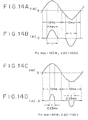
The characteristics illustrated in FIG. 13 are
represented as operation waveform diagrams as seen in
FIGS. 14A to 14D.
-
Here, the ac input voltage VAC and the ac input
current IAC under the conditions of the ac input voltage
VAC = 100 V and the maximum load power Pomax = 120 W are
illustrated in FIGS. 14A and 14B, and the ac input
voltage VAC and the ac input current IAC under the
conditions of the ac input voltage VAC = 100 V and the
minimum load power Pomin = 40 W are illustrated in
FIGS. 14C and 14D.
-
Here, if it is assume that the half period of the
ac input voltage VAC is 10 ms, then when the load power
is the maximum load power Pomax = 120 W, the continuity
period τ of the ac input current IAC actually is
approximately 5 ms and the power factor is PF = 0.85. On
the other hand, when the load power is the minimum load
power Pomin = 40 W, the continuity period τ of the ac
input current IAC decreases to approximately 2.5 ms and
the power factor drops to approximately PF = 0.65. The
value of the power factor PF obtained when the load power
is the minimum load power Pomin = 40 W does not sometimes
satisfy a value of the load factor required for actual
use.
-
Since the power factor is dropped by a variation of
the ac input voltage or a variation of the load power in
this manner, conversely speaking, the ac input voltage or
the load condition to the power supply circuits are
limited. In short, the power supply circuits have a
problem in that apparatus which can adopt the power
supply circuits are limited.
-
More particularly, although the power supply
circuits can be adopted, for example, by a color
television receiver for which the ac input voltage and
the load condition are designated, they cannot be adopted
by business apparatus or information apparatus.
-
Further, it is known that, with the constructions
for power factor improvement shown in FIGS. 10 and 11,
since they adopt the form that the series resonance
circuit on the primary side is connected to the rectified
current path of the commercial ac power supply, ripples
of the commercial ac power supply period (50 Hz/60 Hz)
are superposed on the series resonance circuit. The
superposition level of such ripple components increases
in proportion to increase of the load power.
-
It is known that, for example, if it is assumed
that the power supply circuits are constructed using
required parts selected so that a power factor of
approximately PF = 0.8 may be maintained under
predetermined measurement conditions with which practical
use can be provided, then compared with an alternative
case wherein no power factor improvement circuit is
provided, the ripple voltage level appearing with the
secondary side dc output voltage when the load power is
maximum increases to approximately 3 to 4 times.
-
To suppress such increase of ripple components as
described above, for example, the power supply circuits
shown in FIGS. 10 and 11 actually take such a
countermeasure as augmentation of the gain of the control
circuit 1 or increase of the capacitance of the smoothing
capacitor Ci on the primary side. This, however, gives
rise to problems that the cost of part elements increases
and that the switching operation is liable to suffer from
abnormal oscillation.
-
Various aspects and features of the present invention
are defined in the appended claims.
-
According to
the present invention, there is provided a switching
power supply circuit, comprising rectification smoothing
means for receiving a commercial ac power supply to
produce a rectified smoothed voltage and outputting the
rectified smoothed voltage as a dc input voltage, an
insulation converter transformer having a gap formed
therein so that a coupling coefficient of a loose
coupling may be obtained and provided for transmitting a
primary side output to a secondary side, switching means
for interrupting the dc input voltage by means of a
switching element and outputting the interrupted dc
voltage to a primary winding of the insulation converter
transformer, a primary side resonance circuit formed from
a leakage inductance component at least including the
primary winding of the insulation converter transformer
and a capacitance of a primary side resonance capacitor
for making operation of the switching means operation of
the voltage resonance type, power factor improvement
means inserted in a rectified current path for
interrupting the rectified current based on a switching
output of the switching means fed back to the power factor
improvement means to improve the power factor, a secondary
side resonance circuit formed on the secondary side from a
leakage impedance component of a secondary winding of the
insulation converter transformer and a capacitance of a
secondary side resonance capacitor, dc output voltage
production means formed including the secondary side
resonance circuit for receiving an alternating voltage
obtained at the secondary winding of the insulation
converter transformer and rectifying the alternating
voltage to produce a secondary side dc output voltage, and
constant voltage control means for controlling the
secondary side dc output voltage to a constant voltage in
response to a level of the secondary side dc output
voltage, the primary side resonance capacitor being formed
from a series connection of first and second capacitors,
the switching output of the switching means being fed back
to the power factor improvement means through a connection
point between the first and second capacitors.
-
Embodiments of the present invention relate to a
switching power supply circuit which includes a power
factor improvement circuit.
-
Embodiments of the present invention can provide a
switching power supply which maintains a power factor, or
at least resists a change in power factor, which can
satisfy actual use conditions against a variation in load
or ac input voltage.
-
In the switching power supply circuit, the switching
output of a voltage divided by the primary side resonance
capacitor formed from the series connection of the first
and second capacitors is fed back to the power
factor improvement circuit provided in the power supply
circuit called composite resonance type converter.
-
Consequently, the switching power supply circuit is
advantageous in that the power factor is maintained
constant or at least a change in the power factor is small
over a wide range against a variation of an ac input
voltage or a load power. Consequently, the
switching power supply circuit is suitable as a power
factor improvement power supply circuit for business
apparatus and information apparatus which are ready for a
wide range for use for both of the ac input voltage AC of
a 100 V type and a 200 V type or have a great load
variation.
-
Further, since the switching power supply circuit
exhibits a little increase (or little increase) of a
ripple voltage component such as, for example, a 50 Hz
ripple voltage component in the dc output voltage, no
special countermeasure against ripples is required.
Consequently, the switching power supply circuit is
advantageous also in that augmentation of the gain of a
control circuit, increase of the capacitance of an
electrolytic capacitor or the like is unnecessary.
-
The switching power supply circuit is advantage
further in that, since the dc input voltage rises when
the load is heavy, the efficiency rises when compared
with that before the power factor improvement, and since
the operation waveforms of both of the voltage and the
current become sine waves, generated noise has a low
level.
-
The invention will now be described by way or example
with reference to the accompanying drawings, throughout
which like parts are referred to by like references, and
in which:
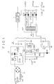
- FIG. 1 is a circuit diagram showing a construction
of a switching power supply circuit according to a first
embodiment of the present invention;
- FIG. 2 is a side elevational sectional view showing
a structure of an insulation converter transformer
adopted by the power supply circuit of FIG. 1;
- FIGS. 3A and 3B are circuit diagrams illustrating
operations of the insulation converter transformer shown
in FIG. 2 when the mutual inductance is +M and -M,
respectively;
- FIGS. 4A to 4F are waveform diagrams illustrating
operation of the switching power supply circuit of
FIG. 1;
- FIGS. 5A to 5D are waveform diagrams illustrating
operation of the switching power supply circuit of
FIG. 1;
- FIG. 6 is a characteristic diagram illustrating a
relationship between a load power and a power factor of
the switching power supply circuit of FIG. 1;
- FIG. 7 is a characteristic diagram illustrating a
relationship of an ac input voltage and a power factor of
the switching power supply circuit of FIG. 1;
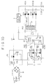
- FIG. 8 is a circuit diagram showing a construction
of a switching power supply circuit according to a second
embodiment of the present invention;
- FIG. 9 is a circuit diagram showing a construction
of a switching power supply circuit according to a third
embodiment of the present invention;
- FIG. 10 is a circuit diagram showing a construction
of a conventional power supply circuit;
- FIG. 11 is a circuit diagram showing a construction
of another conventional power supply circuit;
- FIG. 12 is a characteristic diagram illustrating a
relationship between a load power and a power factor of
the power supply circuits of FIGS. 10 and 11;
- FIG. 13 is a characteristic diagram illustrating a
relationship between an ac input voltage and a power
factor of the power supply circuits of FIGS. 10 and 11;
and
- FIGS. 14A to 14D are waveform diagram illustrating
different operation of the power supply circuits in
response to an input of a commercial ac power supply in
accordance with a load power.
-
-
FIG. 1 is a circuit diagram showing a construction
of a switching power supply circuit as an embodiment of
the present invention. It is to be noted that, in FIG. 1,
like elements to those of FIG. 10 or 11 are denoted by
like reference characters and description of them is
omitted.
-
On the primary side of the power supply circuit
shown in FIG. 1, a switching converter of the voltage
resonance type (voltage resonance type converter) is
provided. And, a power factor improvement circuit is
provided for the voltage resonance type converter.
-
Thus, a construction of the power factor
improvement circuit 10 is hereinafter described, and a
construction of the voltage resonance type converter is
described first.
-
The voltage resonance type converter here adopts a
self-excited scheme which includes a single switching
element Q1. In this instance, a high voltage withstanding
bipolar transistor (BJT; junction transistor) is adopted
for the switching element Q1.
-
The base of the switching element Q1 is connected
to the positive electrode side of a smoothing capacitor
Ci (rectified smoothed voltage Ei) through a starting
resistor RS so that base current upon starting may be
obtained from a rectification smoothing line. Further, a
resonance circuit for self-excited oscillation driving
(self-excited oscillation drive circuit) is connected
between the base of the switching element Q1 and the
primary side ground and is formed from a series
connection circuit including a driving winding NB, a
resonance capacitor CB, and a base current limiting
resistor RB.
-
A clamp diode DD is interposed between the base of
the switching element Q1 and the negative electrode
(primary side ground) of the smoothing capacitor Ci and
forms a path for clamp current which flows when the
switching element Q1 is off.
-
The collector of the switching element Q1 is
connected to the positive terminal of the smoothing
capacitor Ci through a series connection of a detecting
winding ND and a primary winding N1. The emitter of the
switching element Q1 is grounded to the primary side
ground.
-
A pair of capacitors Cr1 and Cr2 connected in
series are connected as a parallel resonance capacitor
between the collector and the emitter of the switching
element Q1. The parallel resonance capacitor Cr (Cr1,
Cr2) forms, based on a capacitance of the parallel
resonance transistor Cr itself and a leakage inductance
L1 of the primary winding N1 of an insulating converter
transformer PIT which is hereinafter described, a primary
side parallel resonance circuit of the voltage resonance
type converter. Although detailed description is omitted
here, when the switching element Q1 is off, an operation
of the voltage resonance type is obtained by an action of
the parallel resonance circuit which causes the voltage
across the resonance capacitor Cr (Cr1, Cr2) to actually
exhibit a pulse wave of a sine waveform.
-
An orthogonal control transformer PRT shown in
FIG. 1 is a saturable reactor which includes the
detection winding ND, the driving winding NB and a
control winding NC wound thereon. The orthogonal control
transformer PRT is provided to drive the switching
element Q1 and perform constant voltage control.
-
The orthogonal control transformer PRT has such a
structure that, though not shown, a three dimensional
core is formed such that two double channel-shaped cores
each having four magnetic legs are joined to each other
at the ends of the magnetic legs thereof. The detection
winding ND and the driving winding NB are wound in the
same winding direction around two predetermined ones of
the magnetic legs of the three dimensional core, and the
control winding NC is wound in a direction orthogonal to
that of the detection winding ND and the driving winding
NB.
-
In this instance, the detection winding ND of the
orthogonal control transformer PRT (frequency variation
means) is connected in series to the primary winding N1
of the insulating converter transformer PIT which is
hereinafter described so that the switching output of the
switching element Q1 is transmitted to the detection
winding ND through the primary winding N1.
-
In the orthogonal control transformer PRT, the
driving winding NB is excited by a switching output
obtained at the detection winding ND through a
transformer coupling so that an alternating voltage as a
drive voltage is generated in the driving winding NB. The
drive voltage is outputted as drive current from the
series resonance circuit (NB, CB), which forms a selfexcited
oscillation drive circuit, to the base of the
switching element Q1 through the base current limiting
circuit RB. Consequently, the switching element Q1
performs a switching operation in a switching frequency
determined by the resonance frequency of the series
resonance circuit (NB, CB).
-
The insulating converter transformer PIT in the
present embodiment includes, as shown in FIG. 2, an EE-shaped
core formed from, for example, a pair of E-shaped
cores CR1 and CR2 made of a ferrite material and combined
such that magnetic poles thereof are opposed to each
other. The primary winding N1 and the secondary winding
N2 are wound in a separate condition from each other on
the central magnetic legs of the EE-shaped core using a
split bobbin B. A gap G is formed between the central
magnetic legs of the EE-shaped core as shown in FIG. 2.
Consequently, a loose coupling having a required coupling
coefficient can be obtained.
-
The gap G can be formed by forming the central
magnetic legs of the E-shaped cores CR1 and CR2 shorter
than the other two outer magnetic legs. The coupling
coefficient k in this instance is, for example, k ≒ 0.85
which is a coupling coefficient of a loose coupling.
Consequently, a saturation condition is less liable to be
obtained as much.
-
An end of the primary winding N1 of the insulation
converter transformer PIT is connected to the collector
of the switching element Q1, and the other end of the
primary winding N1 is connected to the positive electrode
(rectified smoothed voltage Ei) of the smoothing
capacitor Ci through a series connection of the detection
winding ND.
-
On the secondary side of the insulation converter
transformer PIT, an alternating voltage induced by the
primary winding N1 appears in the secondary winding N2.
In this instance, as a secondary side parallel resonance
capacitor C2 is connected in parallel to the secondary
winding N2, a parallel resonance circuit is formed from a
leakage inductance L2 of the secondary winding N2 and a
capacitance of the secondary side parallel resonance
capacitor C2. The alternating voltage induced in the
secondary winding N2 is converted into a resonance
voltage by the parallel resonance circuit. In short, a
voltage resonance operation is obtained on the secondary
side.
-
Thus, in the power supply circuit, a parallel
resonance circuit for making the switching operation a
switching operation of the voltage resonance type is
provided on the primary side, and a parallel resonance
circuit for obtaining a voltage resonance operation is
provided also on the secondary side. It is to be noted
that, in the present specification, a switching converter
of a construction which includes resonance circuits for
both of the primary side and the secondary side in this
manner is suitably referred to as "composite resonance
type switching converter".
-
In this instance, in the parallel resonance circuit
on the secondary side formed in such a manner as
described above, taps are provided for the secondary
winding N2, and rectification diodes D01, D02, D03 and
D04 and smoothing capacitors C01 and C02 are connected in
such a manner as shown in the figure to provide two sets
of full-wave rectification circuits including a set of
the [rectification diodes D01 and D02 and smoothing
capacitor C01] and another set of the [rectification
diodes D03 and D04 and smoothing capacitor C02]. The
full-wave rectification circuit composed of the
[rectification diodes D01 and D02 and smoothing capacitor
C01] produces a dc output voltage E01, and the full-wave
rectification circuit composed of the [rectification
diodes D03 and D04 and smoothing capacitor C02] similarly
produces a dc output voltage E02.
-
It is to be noted that, in this instance, the dc
output voltage E01 and the dc output voltage E02 are
branched and inputted also to a control circuit 1. The
control circuit 1 utilizes the dc output voltage E01 as a
detection voltage and utilizes the dc output voltage E02
as an operation power supply therefor.
-
The control circuit 1 supplies dc current, whose
level varies, for example, in response to the level of
the secondary side dc voltage output E01, as control
current to the control winding NC of the drive
transformer PRT to perform constant voltage control as
hereinafter described.
-
In the insulating converter transformer PIT, the
mutual inductance M between the inductance L1 of the
primary winding N1 and the inductance L2 of the secondary
winding N2 may have a value +M and another value -M
depending upon the relationship between the polarities
(winding directions) of the primary winding N1 and the
secondary winding N2 and the connection of the
rectification diodes D0 (D01, D02, D03, D04).
-
For example, if the components mentioned assume
such a connection configuration as shown in FIG. 3A, then
the mutual inductance M is +M (additive mode: forward
system), but if the components assume such a connection
configuration as shown in FIG. 3B, then the mutual
inductance M is -M (subtractive mode: flyback system).
-
If this is examined in connection with operation of
the secondary side of the power supply circuit shown in
FIG. 1, for example, the operation that rectified current
flows through the rectification diode D01 (D03) when the
alternating voltage obtained at the secondary winding N2
has the positive polarity can be regarded as an operation
mode of +M (forward mode). On the contrary, the operation
that rectified current flows through the rectification
diode D02 (D04) when the alternating voltage obtained at
the secondary winding N2 has the negative polarity can be
regarded as an operation mode of -M (flyback mode). In
other words, the power supply circuit operates in the
+M/-M mode of the mutual inductance each time the
alternating voltage obtained at the secondary winding
becomes positive/negative.
-
As the level of the control current (dc current) to
be supplied to the control winding NC is varied in
response to a variation of the secondary side dc output
voltage level (E01) by the control circuit 1, the
inductance LB of the driving winding NB wound on the
orthogonal control transformer PRT is variably controlled.
Consequently, the resonance condition of the series
resonance circuit in the self-excited oscillation drive
circuit for the switching element Q1 which is formed
including the inductance LB of the driving winding NB
varies. This is an operation of varying the switching
frequency of the switching element Q1, and this operation
acts to stabilize the secondary side dc output voltage.
-
In the circuit shown in FIG. 1, the switching
frequency is to be varied, the period within which the
switching element Q1 is on is variably controlled whereas
the period within which the switching element Q1 is off
is kept fixed. In short, it can be considered that the
power supply apparatus operates, as a constant voltage
controlling operation, to variably control the switching
frequency to perform resonance impedance control for the
switching output, and simultaneously performs continuity
angle control (PWM control) of the switching element in a
switching period. This composite control operation is
realized with a single control circuit system.
-
Here, the switching frequency control is performed
such that, for example, when the secondary side output
voltage rises, for example, due to a tendency of a low
load, the switching frequency is set higher to suppress
the secondary side output.
-
Subsequently, a construction of the power factor
improvement circuit 10 is described.
-
In the power factor improvement circuit 10 shown in
FIG. 1, a filter choke coil LN - high speed recovery type
diode D1 - choke coil LS connected in series are inserted
between a positive output terminal of a bridge
rectification circuit Di and a positive terminal of the
smoothing capacitor Ci.
-
A filter capacitor CN is interposed between the
anode side of the high speed recovery type diode D1 and
the positive terminal of the smoothing capacitor Ci to
form a low-pass filter of a normal mode together with the
filter choke coil LN.
-
In the power factor improvement circuit 10, the
connection point between the capacitors Cr1 and Cr2
connected in series to form the parallel resonance
capacitor described above is connected to a connection
point between the cathode of the high speed recovery type
diode D1 and the choke coil LS so that a switching output
(voltage resonance pulse voltage) supplied to the primary
side parallel resonance circuit may be fed back.
-
The power factor improvement operation of the power
factor improvement circuit 10 basically is such as
described below.
-
In the construction of the power factor improvement
circuit 10 shown in FIG. 1, the switching output supplied
to the primary side parallel resonance circuit is fed
back to the rectified current path through an inductive
reactance (magnetic coupling) which the choke coil LS
itself has.
-
With the switching output fed back in such a manner
as described above, an alternating voltage of the
switching period is superposed on the rectified current
path. By the superposed component of the alternating
voltage of the switching period, an operation of
interrupting the rectified current in the switching
period is obtained at the high speed recovery type diode
D1. By the interruption operation, however, also the
apparent inductance of the filter choke coil LN and the
choke coil LS increases. Consequently, charging current
to the smoothing capacitor Ci flows also within a period
within which the rectified output voltage level is lower
than the voltage across the smoothing capacitor Ci.
-
As a result, an average waveform of the ac input
current approaches the waveform of the ac input voltage
to increase the continuity angle of the ac input current,
and consequently, improvement of the power factor is
achieved.
-
In the present example, the parallel resonance
capacitor Cr which forms the primary side parallel
resonance circuit of the voltage resonance converter of
the primary side is formed from a series connection of
the capacitors Cr1 and Cr2 as described hereinabove, and
the connection point between the capacitors Cr1 and Cr2
is connected to the cathode of the high speed recovery
type diode D1 of the power factor improvement circuit 10.
Accordingly, a circuit system as a voltage feedback
system is formed wherein the voltage resonance pulse
voltage which appears as a voltage across the resonance
capacitor Cr (Cr1 and Cr2) is divided at a ratio in
electrostatic capacitance between the capacitors Cr1 and
Cr2 and is fed back to the connection point between the
high speed recovery type diode D1 and the choke coil LS.
-
The electrostatic capacitances of the capacitors
Cr1 and Cr2 are set to Cr1 < Cr2, and particularly an
increase of the electrostatic capacitance of the
capacitor Cr2 augments the power factor PF.
-
In particular, within a period within which the ac
input voltage VAC is high, the switching frequency fs is
controlled to a high value, but within a period within
which the ac input voltage VAC is low, the switching
frequency fs is controlled to a low value. Consequently,
in the proximity of a peak value of the ac input voltage
VAC, the voltage resonance pulse voltage is not fed back
to the power factor improvement circuit 10, and the ac
input current IAC from the ac power supply AC is charged
into the smoothing capacitor Ci through the bridge
rectification circuit D1 → filter choke coil LN → high
speed recovery type diode D1 → choke coil LS. Then, as
the ac input voltage VAC becomes lower, the feedback
amount of the voltage resonance pulse voltage to the
power factor improvement circuit 10 increases.
-
From this, the ac input voltage VAC, ac input
current IAC, divided voltage V2 by the capacitors Cr1 and
Cr2, current ILS flowing through the choke coil LS,
feedback current I2 and current ID1 flowing through the
high speed recovery type diode D1 exhibit such operation
waveforms as shown in FIGS. 4A to 4F.
-
Meanwhile, the divided voltage V2 by the capacitor
Cr2, current ILS flowing through the choke coil LS,
feedback current I2 and current ID1 flowing through the
high speed recovery type diode D1 in a switching period
at a point of time when the ac input voltage VAC
illustrated in FIG. 4A becomes equal to 0 exhibit such
operation waveforms as shown in FIGS. 5A to 5D,
respectively.
-
It can be seen that, at this time, the operation
waveforms of the current ILS flowing through the choke
coil LS and the feedback current I2 fed back as a voltage
become sine waves due to the series resonance of the
capacitor Cr2 and the choke coil LS.
-
Using the switching power supply circuit of the
present embodiment, an experiment was conducted under the
conditions that the filter choke coil LN = 100 µH, filter
capacitor CN = 1 µF, choke coil LS = 68 µH, capacitor
Cr1 = 4,700 pF, and capacitor Cr2 = 0.022 µF, the load
range from the maximum load power Pomax = 140 W to the
minimum load power Pomin = 0 W and the control range of
the switching frequency fs = 100 KHz to 200 KHz with
respect to the variation of the ac input voltage VAC = 80
V to 140V.
-
As a result, in the state of the ac input voltage
VAC = 100 V, the power factor PF is almost equal to 0.8
with respect to the load variation of the load power Po =
140 W to 20 W as shown in FIG. 6, and is kept fixed.
-
Further, under the condition of the load power Po =
140 W to 20 W with respect to a variation within the
range of the ac input voltage VAC = 80 V to 140 V,
substantially similar power factors were obtained as seen
in FIG. 7.
-
Also the 50 Hz ripple voltage component of the
secondary side dc output voltage level E01 exhibits an
increase of approximately two times that where the power
factor improvement circuit 10 is not provided, and this
is within a range within which there is no problem in
actual use if the switching power supply circuit is used
as a power supply circuit for use with, for example, a
color television or the like.
-
In this manner, the power supply circuit of the
present embodiment can maintain a high power factor
irrespective of a variation of the ac input voltage or
the load. Consequently, it is sufficiently possible in
practical use to incorporate the power supply circuit of
the present embodiment not only in a television receiver
or the like with which ac input voltage and load
conditions are designated but also, for example, in
business apparatus with which a load condition varies and
business apparatus such as a personal computer.
-
Subsequently, a second embodiment of the present
invention is described with reference to FIG. 8.
-
FIG. 8 is a circuit diagram showing a construction
of a power supply circuit according to the second
embodiment of the present invention. It is to be noted
that, in FIG. 8, like elements to those of FIGS. 1, 10
and 11 are denoted by like reference characters and
description thereof is omitted.
-
Further, an insulation converter transformer PIT
shown in FIG. 8 has a structure similar to that shown in
FIG. 11.
-
Referring to FIG. 8, a voltage resonance converter
provided on the primary side has a separate excitation
scheme and includes a switching element Q21 formed from,
for example, a MOS-FET. The drain of the switching
element Q21 is connected to the positive electrode of a
smoothing capacitor Ci through a primary winding N1, and
the source of the switching element Q21 is connected to
the primary side ground.
-
Also in this instance, a parallel resonance
capacitor Cr is formed from a series connection of
capacitors Cr1 and Cr2. An end of the capacitor Cr1 is
connected to the drain of the switching element Q21, and
the other end of the capacitor Cr1 is connected to a
connection point between a high speed recovery type diode
D1 and a choke coil LS of the power factor improvement
circuit 10.
-
Further, the capacitor Cr2 is connected in parallel
to the high speed recovery type diode D1.
-
A clamp diode DD is connected between the drain and
the source of the switching element Q21.
-
The switching element Q21 is driven to switch by an
oscillation drive circuit 2 so that such a switching
operation as described hereinabove with reference to
FIG. 1 may be obtained.
-
In particular, the control circuit 1 supplies
current or voltage of the level which has varied in
response to a variation of the secondary side dc output
voltage E01 to the oscillation drive circuit 2. The
oscillation drive circuit 2 outputs a switching drive
signal (voltage) whose period has been varied in response
to the output level from the control circuit 1 to the
gate of the switching element Q21 so that the secondary
side dc output voltage E01 may be stabilized. The
switching frequency of the switching element Q21 is thus
varied in response the switching drive signal. Thereupon,
a switching drive signal produced so that the period
within which the switching element Q21 is on is varied
whereas the period within which the switching element Q21
is off is fixed as described above is outputted.
-
In this instance, the rectified smoothed voltage Ei
obtained at the smoothing capacitor Ci is supplied as an
operation power supply to a starting circuit 3, and the
starting circuit 3 performs an operation for activating
the oscillation drive circuit 2 with a voltage upon
starting obtained at a winding N4 wound additionally on
the insulation converter transformer PIT.
-
The power factor improvement circuit 10 shown in
FIG. 8 is similar to the power factor improvement circuit
10 described hereinabove with reference to FIG. 1 except
that the capacitor Cr2 described above is connected in
parallel to the high speed recovery type diode D1.
-
Also with such a construction as described above,
similarly as in the embodiment of FIG. 1, the parallel
resonance capacitor Cr which forms the primary side
parallel resonance circuit of the voltage resonance
converter on the primary side is formed from a series
connection of the capacitors Cr1 and Cr2, and the
connection point between the capacitors Cr1 and Cr2 is
connected to the cathode of the high speed recovery type
diode D1 of the power factor improvement circuit 10.
Accordingly, a circuit system as a voltage feedback
system is formed wherein a voltage resonance pulse
voltage which appears as a voltage across the parallel
resonance capacitor Cr (Cr1 and Cr2) is divided at a
ratio in electrostatic capacitance between the capacitors
Cr1 and Cr2 and is fed back to the connection point
between the high speed recovery type diode D1 and the
choke coil LS. The electrostatic capacitances of the
capacitors Cr1 and Cr2 are set to Cr1 < Cr2.
-
Consequently, similarly to the embodiment described
with reference to FIG. 1, a high power factor can be
maintained against a variation of the ac input voltage or
the load. Consequently, it is sufficiently possible in
practical use to incorporate the power supply circuit of
the present embodiment not only in a television receiver
or the like with which ac input voltage and load
conditions are designated but also, for example, in
business apparatus with which a load condition varies and
business apparatus such as a personal computer.
-
By the way, on the secondary side of the power
supply circuit shown in FIG. 8, an end of a secondary
winding N2 is connected to the secondary side ground, and
the other end of the secondary winding N2 is connected to
the connection point between the anode of a rectification
diode D01 and the cathode of a rectification diode D02
through a series connection of a series resonance
capacitor Cs1. The cathode of the rectification diode D01
is connected to the positive electrode of a smoothing
capacitor C01, and the anode of the rectification diode
D01 is connected to the secondary side ground. The
negative electrode side of the smoothing capacitor C01 is
connected to the secondary side ground.
-
According to such a connection scheme as described
above, a double voltage full-wave rectification circuit
formed from a set of the [series resonance capacitor Cs1,
rectification diodes D01 and D02, and smoothing capacitor
C01]. Here, the series resonance capacitor Csl forms a
series resonance circuit corresponding to on/off
operations of the rectification diodes D01 and D02 based
on a capacitance of the series resonance capacitor Cs1
itself and a leakage inductance component of the
secondary winding N2.
-
In other words, the power supply circuit of the
present embodiment has a scheme of a composite resonance
switching converter wherein a parallel resonance circuit
for making the switching operation an operation of the
voltage resonance type is provided on the primary side
and a series resonance circuit for obtaining a double
voltage full-wave rectification operation is provided on
the secondary side.
-
Here, the double voltage full-wave rectification
operation by the set of the [series resonance capacitor
Cs1, rectification diodes D01 and D02, and smoothing
capacitor C01] described above is such as described below.
-
When a switching output is obtained at the primary
winding N1 by a switching operation on the primary side,
the switching output is excited in the secondary winding
N2.
-
Then, within a period within which the
rectification diode D01 is off and the rectification
diode D02 is on, the primary winding N1 and the secondary
winding N2 operate in a subtractive mode wherein the
polarities of them (the mutual inductance M) become -M,
and an operation of charging the series resonance
capacitor Cs1 with the rectified current IC2 rectified by
the rectification diode D02 is obtained by a series
resonance action by the leakage inductance of the
secondary winding N2 and the series resonance capacitor
Cs1.
-
Within another period within which a rectification
operation is performed with the rectification diode D02
turned off and with the rectification diode D01 turned on,
the primary winding N1 and the secondary winding N2
operate in an additive mode wherein the polarities of
them (the mutual inductance M) become +M, and an
operation of charging the smoothing capacitor C01 in a
state wherein series resonance wherein the potential of
the series resonance capacitor Cs1 is added to the
voltage induced in the secondary winding N2 occurs is
performed.
-
Since a rectification operation is performed
utilizing the two modes of the additive mode (+M: forward
operation) and the subtractive mode (-M: flyback
operation) as described above, a dc output voltage E01
equal to substantially twice the induced voltage of the
secondary winding N2 is obtained at the smoothing
capacitor C01.
-
According to the construction described above, on
the secondary side of the circuit shown in FIG. 8, a
secondary side dc output voltage is obtained by
performing double voltage full-wave rectification
utilizing a condition that the two operation modes
wherein the mutual inductance is +M and -M are available.
In particular, electromagnetic energy obtained by a
current resonance action of the primary side and a
current resonance action of the secondary side is
supplied simultaneously to the load side. Consequently,
also the power to be supplied to the load side further
increases, and accordingly, significant increase of the
maximum load power is achieved.
-
Further, since a secondary side dc output voltage
is obtained by the double voltage full-wave rectification
circuit, if it is intended to obtain a level equal to a
secondary side dc output voltage obtained, for example,
by an equal voltage rectification circuit, then the
secondary winding N2 in the present embodiment may have a
number of turns equal to one half a conventional one. The
reduction in number of turns results in reduction of the
size and the weight and reduction of the cost of the
insulation converter transformer PIT.
-
It is to be noted that, in this instance, a
secondary winding N2A is wound independently of the
oscillation drive circuit 2 and a center tap of the
secondary winding N2A is grounded and besides a full wave
rectification circuit formed from rectification diodes
D03 and D04 and a smoothing capacitor C02 is connected so
as to produce a dc output voltage E02.
-
Subsequently, a third embodiment of the present
invention is described with reference to FIG. 9.
-
The switching power supply circuit of FIG. 9 has a
switching converter of the voltage resonance type
(voltage resonance converter) provided on the primary
side thereof basically similarly as in FIG. 1. A power
factor improvement circuit is provided for the voltage
resonance converter.
-
A parallel resonance capacitor Cr which forms a
primary side parallel resonance circuit of a voltage
resonance converter of the primary side is formed from a
serial connection of a pair of capacitors Cr1 and Cr2.
However, the parallel resonance capacitor Cr is different
from that of the embodiment of FIG. 1 in that only the
capacitor Cr1 is connected in parallel between the
collector and the emitter of a switching element Q1 and
the other end of the capacitor Cr2 is connected to the
cathode of a high speed recovery type diode D1 of the
power factor improvement circuit 10.
-
In this instance, the electrostatic capacitances of
the capacitors Cr1 and Cr2 are selected such that that of
the capacitor Cr1 is sufficiently higher than that of the
capacitor Cr2. In other words, the capacitor Cr2 side is
a smaller capacitance capacitor.
-
Also according to the present construction, a
circuit system as a voltage feedback system is formed
wherein a voltage resonance pulse voltage is divided at a
ratio in electrostatic capacitance between the capacitors
Cr1 and Cr2 and is fed back to a connection point between
the high speed recovery type diode D1 and a choke coil LS.
Consequently, similarly to the example described
hereinabove with reference to FIG. 1, a high power factor
can be maintained against a variation of the ac input
voltage or the load.
-
Further, in this instance, a 50 Hz ripple voltage
component of the secondary side dc output voltage E01 is
equivalent to that where the power factor improvement
circuit 10 is not provided, and this does not make a
problem at all in actual use.
-
By the way, on the secondary side of the power
supply circuit of FIG. 9, a secondary side parallel
resonance capacitor C2 is provided for the secondary
winding N2 to form a secondary side parallel resonance
circuit while a rectification smoothing circuit formed
from a bridge rectification circuit DBR and a smoothing
capacitor C01 is provided for the secondary winding N2 to
obtain the secondary side dc output voltage E01. In short,
according the present construction, a full-wave
rectification operation is obtained by the bridge
rectification circuit DBR on the secondary side.
-
It is to be noted that, in this instance, on the
secondary side, another secondary winding N2A is wound
independently of the secondary winding N2 and a center
tap is provided for the secondary winding 2A and besides
rectification diodes D03 and D04 and a smoothing
capacitor C02 are connected in such a manner as seen in
FIG. 9 so as to obtain a secondary side dc output voltage
E02 by a full-wave rectification operation. However, a
parallel resonance capacitor is not provided for the
secondary winding 2A.
-
While the embodiments are described above, the
present invention can be carried out in further various
forms.
-
For example, the applicant of the present
application has already proposed also a construction of a
composite resonance switching converter which includes a
quadruple voltage rectification circuit which makes use
of a secondary side series resonance circuit, and also
such a construction as just described is possible as a
modification to the present embodiment. In short, the
present embodiment is not particularly limited in terms
of the constructions of the resonance circuit and the
rectification circuit on the secondary side.
-
Further, while the voltage resonance converter on
the primary side in the embodiments described above has a
construction of the so-called single end type which
includes a single switching element, the present
invention can be applied also to a voltage resonance
converter of the so-called push-pull type wherein a pair
of switching elements perform switching operations
alternately.
-
While preferred embodiments of the present
invention have been described using specific terms, such
description is for illustrative purposes only, and it is
to be understood that changes and variations may be made
without departing from the scope of the
following claims.