EP1079441A2 - Module de conversion photoélectrique en couche mince et son procédé de fabrication - Google Patents
Module de conversion photoélectrique en couche mince et son procédé de fabrication Download PDFInfo
- Publication number
- EP1079441A2 EP1079441A2 EP00103474A EP00103474A EP1079441A2 EP 1079441 A2 EP1079441 A2 EP 1079441A2 EP 00103474 A EP00103474 A EP 00103474A EP 00103474 A EP00103474 A EP 00103474A EP 1079441 A2 EP1079441 A2 EP 1079441A2
- Authority
- EP
- European Patent Office
- Prior art keywords
- cells
- series
- module
- photoelectric conversion
- thin film
- Prior art date
- Legal status (The legal status is an assumption and is not a legal conclusion. Google has not performed a legal analysis and makes no representation as to the accuracy of the status listed.)
- Ceased
Links
- 238000006243 chemical reaction Methods 0.000 title claims abstract description 148
- 239000010409 thin film Substances 0.000 title claims abstract description 140
- 238000004519 manufacturing process Methods 0.000 title claims description 10
- 229910052751 metal Inorganic materials 0.000 claims abstract description 101
- 239000002184 metal Substances 0.000 claims abstract description 101
- 239000000758 substrate Substances 0.000 claims abstract description 66
- 238000003491 array Methods 0.000 claims abstract description 48
- 238000010276 construction Methods 0.000 claims abstract description 18
- 238000000034 method Methods 0.000 claims description 15
- 229910052724 xenon Inorganic materials 0.000 claims description 12
- FHNFHKCVQCLJFQ-UHFFFAOYSA-N xenon atom Chemical compound [Xe] FHNFHKCVQCLJFQ-UHFFFAOYSA-N 0.000 claims description 12
- 239000000463 material Substances 0.000 claims description 7
- 229910052757 nitrogen Inorganic materials 0.000 claims description 2
- 239000010410 layer Substances 0.000 description 148
- 239000010408 film Substances 0.000 description 54
- XOLBLPGZBRYERU-UHFFFAOYSA-N tin dioxide Chemical compound O=[Sn]=O XOLBLPGZBRYERU-UHFFFAOYSA-N 0.000 description 30
- UFHFLCQGNIYNRP-UHFFFAOYSA-N Hydrogen Chemical compound [H][H] UFHFLCQGNIYNRP-UHFFFAOYSA-N 0.000 description 18
- 229910052739 hydrogen Inorganic materials 0.000 description 18
- 239000001257 hydrogen Substances 0.000 description 18
- 230000001678 irradiating effect Effects 0.000 description 12
- 229910021417 amorphous silicon Inorganic materials 0.000 description 11
- 229920005989 resin Polymers 0.000 description 11
- 239000011347 resin Substances 0.000 description 11
- 239000004065 semiconductor Substances 0.000 description 9
- HBMJWWWQQXIZIP-UHFFFAOYSA-N silicon carbide Chemical compound [Si+]#[C-] HBMJWWWQQXIZIP-UHFFFAOYSA-N 0.000 description 9
- 239000012535 impurity Substances 0.000 description 8
- 238000004544 sputter deposition Methods 0.000 description 8
- 230000003247 decreasing effect Effects 0.000 description 7
- 230000000694 effects Effects 0.000 description 7
- 238000010248 power generation Methods 0.000 description 7
- 230000001681 protective effect Effects 0.000 description 7
- XUIMIQQOPSSXEZ-UHFFFAOYSA-N Silicon Chemical compound [Si] XUIMIQQOPSSXEZ-UHFFFAOYSA-N 0.000 description 6
- 229910021424 microcrystalline silicon Inorganic materials 0.000 description 6
- 229910052710 silicon Inorganic materials 0.000 description 6
- 239000010703 silicon Substances 0.000 description 6
- 230000000052 comparative effect Effects 0.000 description 5
- 239000005038 ethylene vinyl acetate Substances 0.000 description 5
- 239000011521 glass Substances 0.000 description 5
- 230000002093 peripheral effect Effects 0.000 description 5
- 229920001200 poly(ethylene-vinyl acetate) Polymers 0.000 description 5
- ZOXJGFHDIHLPTG-UHFFFAOYSA-N Boron Chemical compound [B] ZOXJGFHDIHLPTG-UHFFFAOYSA-N 0.000 description 4
- OAICVXFJPJFONN-UHFFFAOYSA-N Phosphorus Chemical compound [P] OAICVXFJPJFONN-UHFFFAOYSA-N 0.000 description 4
- 229910052782 aluminium Inorganic materials 0.000 description 4
- XAGFODPZIPBFFR-UHFFFAOYSA-N aluminium Chemical compound [Al] XAGFODPZIPBFFR-UHFFFAOYSA-N 0.000 description 4
- 229910052796 boron Inorganic materials 0.000 description 4
- NBVXSUQYWXRMNV-UHFFFAOYSA-N fluoromethane Chemical compound FC NBVXSUQYWXRMNV-UHFFFAOYSA-N 0.000 description 4
- 239000011888 foil Substances 0.000 description 4
- 238000010438 heat treatment Methods 0.000 description 4
- 230000000977 initiatory effect Effects 0.000 description 4
- 229910052698 phosphorus Inorganic materials 0.000 description 4
- 239000011574 phosphorus Substances 0.000 description 4
- 238000005268 plasma chemical vapour deposition Methods 0.000 description 4
- 238000007789 sealing Methods 0.000 description 4
- 229910010271 silicon carbide Inorganic materials 0.000 description 4
- 229910000676 Si alloy Inorganic materials 0.000 description 3
- 229910000577 Silicon-germanium Inorganic materials 0.000 description 3
- LEVVHYCKPQWKOP-UHFFFAOYSA-N [Si].[Ge] Chemical compound [Si].[Ge] LEVVHYCKPQWKOP-UHFFFAOYSA-N 0.000 description 3
- 229910021419 crystalline silicon Inorganic materials 0.000 description 3
- 230000008018 melting Effects 0.000 description 3
- 238000002844 melting Methods 0.000 description 3
- 239000002356 single layer Substances 0.000 description 3
- XLYOFNOQVPJJNP-UHFFFAOYSA-N water Substances O XLYOFNOQVPJJNP-UHFFFAOYSA-N 0.000 description 3
- IJGRMHOSHXDMSA-UHFFFAOYSA-N Atomic nitrogen Chemical compound N#N IJGRMHOSHXDMSA-UHFFFAOYSA-N 0.000 description 2
- RYGMFSIKBFXOCR-UHFFFAOYSA-N Copper Chemical compound [Cu] RYGMFSIKBFXOCR-UHFFFAOYSA-N 0.000 description 2
- 229920002367 Polyisobutene Polymers 0.000 description 2
- 230000015572 biosynthetic process Effects 0.000 description 2
- 230000015556 catabolic process Effects 0.000 description 2
- 239000004020 conductor Substances 0.000 description 2
- 239000011889 copper foil Substances 0.000 description 2
- 238000010586 diagram Methods 0.000 description 2
- 230000003292 diminished effect Effects 0.000 description 2
- 230000020169 heat generation Effects 0.000 description 2
- 238000009413 insulation Methods 0.000 description 2
- 229920002037 poly(vinyl butyral) polymer Polymers 0.000 description 2
- 229910052709 silver Inorganic materials 0.000 description 2
- 239000004332 silver Substances 0.000 description 2
- 238000007740 vapor deposition Methods 0.000 description 2
- 125000000391 vinyl group Chemical group [H]C([*])=C([H])[H] 0.000 description 2
- 229920002554 vinyl polymer Polymers 0.000 description 2
- 229920002799 BoPET Polymers 0.000 description 1
- VYZAMTAEIAYCRO-UHFFFAOYSA-N Chromium Chemical compound [Cr] VYZAMTAEIAYCRO-UHFFFAOYSA-N 0.000 description 1
- YCKRFDGAMUMZLT-UHFFFAOYSA-N Fluorine atom Chemical compound [F] YCKRFDGAMUMZLT-UHFFFAOYSA-N 0.000 description 1
- 238000005229 chemical vapour deposition Methods 0.000 description 1
- 229910052804 chromium Inorganic materials 0.000 description 1
- 239000011651 chromium Substances 0.000 description 1
- 230000002950 deficient Effects 0.000 description 1
- 238000000151 deposition Methods 0.000 description 1
- 239000002019 doping agent Substances 0.000 description 1
- 210000003608 fece Anatomy 0.000 description 1
- 229910052731 fluorine Inorganic materials 0.000 description 1
- 239000011737 fluorine Substances 0.000 description 1
- 239000007792 gaseous phase Substances 0.000 description 1
- 238000003475 lamination Methods 0.000 description 1
- 229920002620 polyvinyl fluoride Polymers 0.000 description 1
- 239000011241 protective layer Substances 0.000 description 1
- 150000003376 silicon Chemical class 0.000 description 1
- 239000002210 silicon-based material Substances 0.000 description 1
- 229920002050 silicone resin Polymers 0.000 description 1
- 238000005476 soldering Methods 0.000 description 1
- 229920005992 thermoplastic resin Polymers 0.000 description 1
- 229920001187 thermosetting polymer Polymers 0.000 description 1
- 229910052720 vanadium Inorganic materials 0.000 description 1
- LEONUFNNVUYDNQ-UHFFFAOYSA-N vanadium atom Chemical compound [V] LEONUFNNVUYDNQ-UHFFFAOYSA-N 0.000 description 1
Images
Classifications
-
- H—ELECTRICITY
- H01—ELECTRIC ELEMENTS
- H01L—SEMICONDUCTOR DEVICES NOT COVERED BY CLASS H10
- H01L31/00—Semiconductor devices sensitive to infrared radiation, light, electromagnetic radiation of shorter wavelength or corpuscular radiation and specially adapted either for the conversion of the energy of such radiation into electrical energy or for the control of electrical energy by such radiation; Processes or apparatus specially adapted for the manufacture or treatment thereof or of parts thereof; Details thereof
- H01L31/18—Processes or apparatus specially adapted for the manufacture or treatment of these devices or of parts thereof
- H01L31/186—Particular post-treatment for the devices, e.g. annealing, impurity gettering, short-circuit elimination, recrystallisation
-
- H—ELECTRICITY
- H01—ELECTRIC ELEMENTS
- H01L—SEMICONDUCTOR DEVICES NOT COVERED BY CLASS H10
- H01L27/00—Devices consisting of a plurality of semiconductor or other solid-state components formed in or on a common substrate
- H01L27/14—Devices consisting of a plurality of semiconductor or other solid-state components formed in or on a common substrate including semiconductor components sensitive to infrared radiation, light, electromagnetic radiation of shorter wavelength or corpuscular radiation and specially adapted either for the conversion of the energy of such radiation into electrical energy or for the control of electrical energy by such radiation
- H01L27/142—Energy conversion devices
- H01L27/1421—Energy conversion devices comprising bypass diodes integrated or directly associated with the device, e.g. bypass diode integrated or formed in or on the same substrate as the solar cell
-
- H—ELECTRICITY
- H01—ELECTRIC ELEMENTS
- H01L—SEMICONDUCTOR DEVICES NOT COVERED BY CLASS H10
- H01L31/00—Semiconductor devices sensitive to infrared radiation, light, electromagnetic radiation of shorter wavelength or corpuscular radiation and specially adapted either for the conversion of the energy of such radiation into electrical energy or for the control of electrical energy by such radiation; Processes or apparatus specially adapted for the manufacture or treatment thereof or of parts thereof; Details thereof
- H01L31/02—Details
- H01L31/02016—Circuit arrangements of general character for the devices
- H01L31/02019—Circuit arrangements of general character for the devices for devices characterised by at least one potential jump barrier or surface barrier
- H01L31/02021—Circuit arrangements of general character for the devices for devices characterised by at least one potential jump barrier or surface barrier for solar cells
-
- H—ELECTRICITY
- H01—ELECTRIC ELEMENTS
- H01L—SEMICONDUCTOR DEVICES NOT COVERED BY CLASS H10
- H01L31/00—Semiconductor devices sensitive to infrared radiation, light, electromagnetic radiation of shorter wavelength or corpuscular radiation and specially adapted either for the conversion of the energy of such radiation into electrical energy or for the control of electrical energy by such radiation; Processes or apparatus specially adapted for the manufacture or treatment thereof or of parts thereof; Details thereof
- H01L31/04—Semiconductor devices sensitive to infrared radiation, light, electromagnetic radiation of shorter wavelength or corpuscular radiation and specially adapted either for the conversion of the energy of such radiation into electrical energy or for the control of electrical energy by such radiation; Processes or apparatus specially adapted for the manufacture or treatment thereof or of parts thereof; Details thereof adapted as photovoltaic [PV] conversion devices
- H01L31/042—PV modules or arrays of single PV cells
- H01L31/0445—PV modules or arrays of single PV cells including thin film solar cells, e.g. single thin film a-Si, CIS or CdTe solar cells
- H01L31/046—PV modules composed of a plurality of thin film solar cells deposited on the same substrate
-
- Y—GENERAL TAGGING OF NEW TECHNOLOGICAL DEVELOPMENTS; GENERAL TAGGING OF CROSS-SECTIONAL TECHNOLOGIES SPANNING OVER SEVERAL SECTIONS OF THE IPC; TECHNICAL SUBJECTS COVERED BY FORMER USPC CROSS-REFERENCE ART COLLECTIONS [XRACs] AND DIGESTS
- Y02—TECHNOLOGIES OR APPLICATIONS FOR MITIGATION OR ADAPTATION AGAINST CLIMATE CHANGE
- Y02E—REDUCTION OF GREENHOUSE GAS [GHG] EMISSIONS, RELATED TO ENERGY GENERATION, TRANSMISSION OR DISTRIBUTION
- Y02E10/00—Energy generation through renewable energy sources
- Y02E10/50—Photovoltaic [PV] energy
-
- Y—GENERAL TAGGING OF NEW TECHNOLOGICAL DEVELOPMENTS; GENERAL TAGGING OF CROSS-SECTIONAL TECHNOLOGIES SPANNING OVER SEVERAL SECTIONS OF THE IPC; TECHNICAL SUBJECTS COVERED BY FORMER USPC CROSS-REFERENCE ART COLLECTIONS [XRACs] AND DIGESTS
- Y02—TECHNOLOGIES OR APPLICATIONS FOR MITIGATION OR ADAPTATION AGAINST CLIMATE CHANGE
- Y02P—CLIMATE CHANGE MITIGATION TECHNOLOGIES IN THE PRODUCTION OR PROCESSING OF GOODS
- Y02P70/00—Climate change mitigation technologies in the production process for final industrial or consumer products
- Y02P70/50—Manufacturing or production processes characterised by the final manufactured product
-
- Y—GENERAL TAGGING OF NEW TECHNOLOGICAL DEVELOPMENTS; GENERAL TAGGING OF CROSS-SECTIONAL TECHNOLOGIES SPANNING OVER SEVERAL SECTIONS OF THE IPC; TECHNICAL SUBJECTS COVERED BY FORMER USPC CROSS-REFERENCE ART COLLECTIONS [XRACs] AND DIGESTS
- Y10—TECHNICAL SUBJECTS COVERED BY FORMER USPC
- Y10S—TECHNICAL SUBJECTS COVERED BY FORMER USPC CROSS-REFERENCE ART COLLECTIONS [XRACs] AND DIGESTS
- Y10S136/00—Batteries: thermoelectric and photoelectric
- Y10S136/291—Applications
- Y10S136/293—Circuits
Definitions
- the present invention relates to a thin film photoelectric conversion module and a method of manufacturing the same, particularly, to a thin film photoelectric conversion module having a plurality of thin film photoelectric conversion cells connected in series and a method of manufacturing the same.
- a thin film photoelectric conversion module comprises a plurality of band-like thin film photoelectric conversion cells arranged in the direction of the short axis of the cell and connected to each other in series.
- a module is not used singly and is used generally in the form of a module array consisting of a plurality of modules connected in series or in parallel.
- the light to the particular cell is partially or entirely intercepted so as to decrease the photoelectromotive force, leading to a marked reduction in the output of the entire module.
- the cell with the decreased photoelectromotive force acts as a diode connected in series in the reverse direction to the direction of the power generation, i.e., in the reverse direction to the direction in which the current generated by the photoelectric conversion flows.
- the light-intercepted cell exhibits a very high resistance, leading to the marked reduction in the output of the entire module as pointed out above.
- the decreased photoelectromotive force of the cell affects not only the particular module but also the module array. More specifically, the module including a cell whose photoelectromotive force is decreased causes the output of the module array to be lowered markedly.
- a measure for overcoming the problem is disclosed in, for example, Japanese Patent Disclosure (Kokai) No. 57-53986. Specifically, it is disclosed that a plurality of thin film photoelectric conversion cells connected in series are divided into a plurality of series arrays, and that these series arrays are connected in parallel. The particular technique makes it possible to prevent the output of the module array from being lowered markedly even if the photoelectromotive force of any of the cells has become zero. Also, in order to prevent the output of the module array from being lowered markedly, another measure such as mounting a single bypass diode to every module is known.
- an additional problem is produced by the attachment of, for example, a leaf to the thin film photoelectric conversion cell, as follows. Specifically, if voltage higher than the withstand voltage is applied to the cell having the light thereto intercepted by the attached leaf or the like, an insulation breakdown is generated. Current does not flow uniformly through the cell of the particular state so as to bring about a local heating called a hot spot phenomenon. The local heating does not produce a serious problem where the current flowing through the cell is small.
- a module having a large area generally produces a large output current, with the result that, in the conventional module having a large area, the light-intercepted cell is heated to a very high temperature.
- An object of the present invention is to provide a thin film photoelectric conversion module in which, even if the light to one of the thin film photoelectric conversion cells is intercepted, the particular cell is not heated to an excessively high temperature, and a method of manufacturing the particular module.
- Another object is to suppress the heating of a thin film photoelectric conversion cell where the light to one of the cells is intercepted so as to prevent the particular cell from being broken.
- Still another object of the present invention is to provide a thin film photoelectric conversion module having a high reliability and a method of manufacturing the same.
- a thin film photoelectric conversion module of a high reliability comprising a plurality of thin film photoelectric conversion cells can be achieved by suppressing the behavior of the cell as a diode, by preventing a large current from flowing through the light-intercepted cell, or by facilitating the formation of a short-circuit in the light-intercepted cell.
- the cell having the light thereto intercepted can be prevented from being heated to an excessively high temperature.
- the light-intercepted cell is capable of easily permitting a current to flow in the direction equal to the power generating direction.
- a current is not allowed to flow through the light-intercepted cell
- the heat generation in the cell can be suppressed so as to prevent the cell from being broken.
- the short-circuiting can be generated at a relatively low temperature, making it possible to prevent the cell from being heated to an excessively high temperature.
- the present inventors have conducted an extensive research in suppressing the behavior of the light-intercepted cell as a diode. As a result, a special phenomenon has been found that, where a reversed bias, i.e., voltage in the forward direction relative to the power generation direction, is applied repeatedly to the thin film photoelectric conversion cell, it is possible to increase the current flowing through the cell on applying a reversed bias voltage while scarcely affecting the fill factor (F.F.).
- the present inventors considered that, even if light to a certain cell was intercepted, it would be possible to prevent the light-intercepted cell from being heated to an excessively high temperature, to prevent the output of the entire module from being markedly lowered, and to prevent the cell from being broken by utilizing the particular phenomenon pointed out above. These effects have been actually confirmed.
- a thin film photoelectric conversion module comprising a substrate; and a series-connected array including a plurality of thin film photoelectric conversion cells formed on the substrate and connected to each other in series, the number of cells being represented by N, an open-circuit voltage of each the cells being represented by E, and N being an integer of at least 10, wherein a current equal to a short-circuit current of each of the cells under conditions that a xenon lamp is used as a light source, an irradiance is 100 mW/cm 2 , air mass is 1.5, and temperature is 25°C, is allowed to flow through each of the cells by application of a reversed bias voltage not higher than (N-1) ⁇ E .
- a method of manufacturing a thin film photoelectric conversion module including a substrate and a plurality of thin film photoelectric conversion cells formed on the substrate and connected to each other in forward direction, comprising the step of repeatedly applying a reversed bias voltage to each of the cells so as to increase the magnitude of the current flowing through the cells on applying the reversed bias voltage.
- the reversed bias voltage is, for example, not higher than 8V.
- the cells are generally connected in series to form a series-connected array.
- the predetermined state denotes the state that, when the reversed bias voltage represented by (N-1) ⁇ E , e.g., reversed bias voltage of about 8V, is applied to the cell, the current flowing through the cell is not smaller than the short-circuit current of the series-connected array under the above-noted conditions. Even if the light to one of the cells is intercepted in the module thus obtained, the light-intercepted cell is not heated excessively so as to be broken. Also, in this case, it is desirable to apply repeatedly a reversed bias voltage of 8V to 9V to each cell.
- the present inventors have also conducted an extensive research in an attempt to prevent a large current from flowing through the light-intercepted cell.
- the construction that a plurality of series-connected arrays are connected in parallel and by designing the short-circuit current of each array at a value not higher a predetermined value the light-intercepted cell can be prevented from being heated to an excessively high temperature so as to prevent the cell from being broken even where a photoelectromotive force is not generated from one of the thin film photoelectric conversion cells.
- a thin film photoelectric conversion module comprising a substrate, a plurality of series-connected arrays each including a plurality of thin film photoelectric conversion cells formed on the substrate and connected in series, and a pair of common electrodes for connecting these plural series-connected arrays in parallel, wherein a short-circuit current of the module is not lower than 1A under conditions that a xenon lamp is used as a light source, irradiance is 100 mW/cm 2 , air mass is 1.5, and temperature is 25°C, and a short-circuit current of each of the plural series-connected array is not higher than 600 mA under the above-noted conditions.
- these cells are arranged, for example, in both the vertical and lateral directions to form a lattice-like arrangement.
- the cells adjacent to each other in the vertical direction are connected in series to form the plural series-connected arrays, and the pair of common electrodes are arranged in both edge portions in the vertical direction of the particular arrangement of the cells.
- the short-circuit current of each of the plural series-connected arrays is not higher than 300 mA under the conditions given above.
- the light-intercepted cell is prevented from being heated to an excessively high temperature so as to effectively prevent the cell from being broken.
- the present inventors paid attentions to the fact described below. Specifically, if a series-connected array consisting of an N-number of thin film photoelectric conversion cells connected in series is short-circuited in the case where the light to one of the cells is intercepted, voltage obtained by multiplying the open-circuit voltage V b of each cell by (N-1) is applied to the light-intercepted cell. In this case, if the voltage (N-1) ⁇ V b is not higher than the withstand voltage V a of each cell, it is possible to prevent a large current from flowing locally through the cell that has lost its photoelectromotive force. However, the voltage (N-1) ⁇ V b is generally higher than the withstand voltage V a of each cell.
- the present inventors have found that, by dividing the series-connected array into a plurality of sub-arrays and by connecting in parallel a bypass diode to each of these sub-arrays, it is possible to lower the voltage applied to the cell that has lost its photoelectromotive force because of occurrence of the above-noted problem. It has also been found that, if the number N s of the cells constituting each sub-array meets the relationship (N s -1) ⁇ V b ⁇ V a , it is possible to prevent the cell that has lost its photoelectromotive force from being heated to an excessively high temperature so as to prevent the particular cell from being broken.
- a thin film photoelectric conversion module comprising a substrate; a plurality of sub-arrays each having a plurality of thin film photoelectric conversion cells formed on the substrate and connected in series, the number of cells constituting each of the plural sub-arrays being represented by N s and the plural sub-arrays being connected in series to form a series-connected array; and a plurality of bypass diodes connected in parallel to the plural sub-arrays, respectively, wherein the number N s , withstand voltage V a of each of the cells, and each open-circuit voltage V b of the cells under conditions that a xenon lamp is used as light source, irradiance is 100 mW/cm 2 , air mass is 1.5, and temperature is 25°C, meet an inequality N s ⁇ V a /V b + 1 .
- each of the plural bypass diodes is, for example, a thin film formed on main surface of the substrate.
- each of these bypass diodes may be equal in the layer construction to the cell.
- the number N s , the withstand voltage V a , and the open-circuit voltage V b meet an inequality V a /V b -1 ⁇ N s .
- the light-intercepted cell is prevented from being heated excessively and, thus, is effectively prevented from being broken.
- a conductive transparent oxide layer is formed in general between the thin film photoelectric conversion unit and the metal back surface electrode layer in an attempt to improve the bonding strength between the two.
- the transparent oxide has in general a melting point higher than that of a metal. Therefore, in the conventional thin film photoelectric conversion cell, the short-circuiting between the metal back surface electrode layer and the transparent front surface electrode layer is obstructed so as to cause the cell to be heated to a very high temperature.
- the present inventors have found that, if the metal back surface electrode layer and the thin film photoelectric conversion unit is brought into contact with each other in a part of the region positioned between the metal back surface electrode layer and the transparent front surface electrode layer, it is possible to bring about short-circuiting between the metal back surface electrode layer and the transparent front surface electrode layer instantly a large current flows locally through the cell while maintaining a high bonding strength between the unit and the metal back surface electrode layer. It has also been found that a similar effect can be obtained if a metal portion is arranged in contact with the thin film photoelectric conversion unit in a part of the region interposed between the metal back surface electrode layer and the transparent front surface electrode layer.
- a thin film photoelectric conversion module comprising a substrate; and a plurality of thin film photoelectric conversion cells formed on the substrate and connected in series, wherein each of the cells comprises a transparent front surface electrode layer, a thin film photoelectric conversion unit provided on the transparent front surface electrode, a conductive transparent oxide layer provided on the unit, a metal back surface electrode layer provided on the transparent oxide layer, and a metal portion that is partly brought into contact with the unit in a region sandwiched between the transparent front surface electrode layer and the metal back surface electrode layer.
- the contact area between the thin film photoelectric conversion unit and the metal portion is 0.5 to 10% of a surface area of the unit in the region sandwiched between the transparent front surface electrode layer and the metal back surface electrode layer. In this case, occurrence of the short-circuiting of the light-intercepted cell can be facilitated while scarcely sacrificing, for example, the bonding strength between the thin film photoelectric conversion unit and the metal back surface electrode layer.
- the metal portion can be arranged such that the metal portion is in contact with the back surface of the thin film photoelectric conversion unit and that the metal portion communicates with both the unit and the metal back surface electrode layer.
- the metal portion can be formed of the same material as that constituting the metal back surface electrode layer.
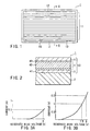
- FIG. 1 is a plan view schematically showing a thin film photoelectric conversion module 1 according to a first embodiment of the present invention.
- the module 1 comprises a transparent substrate 2 and band-like thin film photoelectric conversion cells 10 arranged on the substrate 2. These thin film photoelectric conversion cells 10 are connected to each other in series in the direction of the short axis of the cell 10 to form a series-connected array 11.
- a pair of electrode bus bars 12 each consisting of a ribbon-like copper foil or the like are connected as common electrodes to both ends of the series-connected array 11.
- FIG. 2 which is a cross sectional view along the line II-II shown in FIG. 1, shows in detail the construction of the module 1 shown in FIG. 1. Only a part of the module 1 is depicted in FIG. 2.
- the cell 10 of the module 1 comprises the transparent substrate 2.
- Laminated on the substrate 2 are a transparent front surface electrode layer 3, a thin film photoelectric conversion unit 4 and a metal back surface electrode layer 5.
- the light incident on the transparent substrate 2 is subjected to a photoelectric conversion by the photoelectric conversion unit 4.
- the transparent substrate 2 can be formed of, for example, a glass plate or a transparent resin film.
- the transparent front surface electrode layer 3 formed on the transparent substrate 2 can be formed of an ITO film, an SnO 2 film or a transparent conductive oxide film such as a ZnO film.
- the electrode layer 3 may be of a single layer structure or a multi-layer structure, and can be formed by a gaseous phase deposition method known to the art such as a vacuum vapor deposition method, a CVD method, and a sputtering method.
- the transparent front surface electrode layer 3 prefferably has a surface texture structure having a fine irregularity.
- the particular surface structure of the electrode layer 3 permits improving the incident efficiency of the light on the photoelectric conversion unit 4.
- the thin film photoelectric conversion unit 4 formed on the transparent front surface electrode layer 3 is of a laminate structure consisting, for example, of a p-type non-single crystalline silicon-based semiconductor layer 41, a non-single crystalline thin film photoelectric conversion layer 42 and an n-type non-single crystalline silicon-based semiconductor layer 43 as shown in FIG. 2.
- a p-type non-single crystalline silicon-based semiconductor layer 41 a non-single crystalline thin film photoelectric conversion layer 42 and an n-type non-single crystalline silicon-based semiconductor layer 43 as shown in FIG. 2.
- Each of these p-type semiconductor layer 41, photoelectric conversion layer 42 and n-type semiconductor layer 43 can be formed by a plasma CVD method.
- the p-type silicon-based semiconductor layer 41 can be formed by doping silicon or a silicon alloy such as silicon carbide and silicon-germanium with a p-type impurity such as boron or aluminum.
- the photoelectric conversion layer 42 positioned on the p-type semiconductor layer 41 is formed of a non-single crystalline silicon-based material including, for example, an intrinsic silicon semiconductor such as a hydrogenated silicon, a silicon alloy such as silicon carbide and silicon-germanium. It is also possible to use a weakly p-type or weakly n-type silicon-based semiconductor material containing traces of a dopant for determining the conductivity type as far as the photoelectric conversing function is sufficiently performed.
- the n-type silicon-based semiconductor layer 43 positioned on the photoelectric conversion layer 42 is formed by doping silicon, a silicon alloy such as silicon carbide and silicon-germanium with an impurity for determining the n-type conductivity such as phosphorus or nitrogen.
- the metal back surface electrode layer 5 formed on the photoelectric conversion unit 4 functions as an electrode and as a reflecting layer for reflecting the light incident from the transparent substrate 2 on the photoelectric conversion unit 4 to permit the reflected light to be incident again on the photoelectric conversion unit 4.
- the metal back surface electrode layer 5, which consists of, for example, silver, can be formed by a vacuum vapor deposition method, a sputtering method, etc.
- a transparent oxide layer (not shown) consisting of a conductive transparent oxide such as ZnO is formed between the metal back surface electrode layer 5 and the photoelectric conversion unit 4 in order to improve the bonding strength between the two.
- the transparent oxide layer which generally has a thickness of 50 nm to 150 nm, can be formed by, for example, a sputtering method.
- the transparent front surface electrode layer 3 is formed first in the form a sheet and, then, divided by a laser scribing using, for example, a YAG laser. Then, the thin film photoelectric conversion unit 4 is formed in the form of a sheet on the electrode layer 3, followed by dividing the photoelectric conversion unit 4 by the laser scribing. Further, the metal back surface electrode layer 5 is formed in the form of a sheet on the photoelectric conversion unit 4, followed by dividing the electrode layer 5 by the laser scribing. As a result, formed are the plural thin film photoelectric conversion cells 10 connected in series as shown in FIG. 1. In this embodiment, a reversed bias voltage is repeatedly applied to these thin film photoelectric conversion cells 10.
- FIGS. 3A and 3B are graph showing the relationship between the reversed bias voltage applied to the photoelectric conversion cell 10 and the current flowing through the cell 10.
- FIG. 3A covers the state before a reversed bias voltage is repeatedly applied to the cell 10, with FIG. 3B covering the state after a reversed bias voltage is repeatedly applied to the cell 10.
- a reversed bias voltage applied to the cell 10 is plotted on the abscissa. Also, the current flowing through the cell 10 is plotted on the ordinate.
- the current flowing through the cell 10 is increased, if a reversed bias voltage is repeatedly applied to the cell 10.
- the resistance is decreased when the light to the cell 10 is intercepted.
- the particular treatment makes it possible to prevent the output of the module 1 from being lowered markedly even if the light to one of the cells 10 is completely intercepted.
- the current is allowed to flow relatively uniformly when the light to the cell 10 is intercepted.
- the local heating within the cell 10 is suppressed so as to prevent the cell 10 from being broken on the basis of the hot spot phenomenon.
- the effect produced by the reversed bias treatment can be obtained without sacrificing the F.F. characteristics of the cell 10. It follows that the reversed bias treatment employed in the present invention makes it possible to achieve good F.F. characteristics and a high reliability simultaneously.
- the resistance of the cell 10 when the light to the cell 10 is intercepted is decreased in general with increase in the number of times of applying the reversed bias voltage, finally reaching a saturation.
- the aimed resistance differs depending on the construction of the module 1.
- N being an integer of at least 10
- E the open-circuit voltage of the cell 10 under the conditions given below
- each of the cells 10 under the conditions given above is 0.8V to 0.9V and the series-connected array 11 consists of 10 thin film photoelectric conversion cells 10 connected in series, it suffices to apply a reversed bias voltage repeatedly until the current at the time when a reversed bias voltage of 8V is applied to each of the thin film photoelectric conversion cells 10 is increased to exceed the short-circuit current of the series-connected array 11 under the conditions given above.
- the reversed bias treatment it is desirable to apply the reversed bias treatment to the module 1 having the series-connected array 11 consisting of a large number of thin film photoelectric conversion cells 10, for example at least 20 cells 10.
- a higher reversed bias voltage is applied to a cell 10 where the light to the cell 10 is intercepted, and therefore the cell 10 is easy to be broken. It follows that the reversed bias treatment is more effective when applied to such a module.
- each cell permits the current equal to the short-circuit current under the above-noted conditions of the series-connected array to flow in the direction equal to the power generation direction with a lower reversed bias voltage, e.g., a reversed bias voltage not higher than 7V.
- a reversed bias voltage e.g., a reversed bias voltage not higher than 7V.
- the reversed bias voltage applied repeatedly to the cell 10 should be set to fall within a range within which the cell 10 is not broken and the resistance of the light-intercepted cell can be decreased.
- the particular range, which differs depending on the construction, etc. of the cell 10, covers generally 8V to 9V.
- the reversed bias voltage can be applied to the cell 10 by bringing a pair of conductive portions connected to a power source into contact with the metal back surface electrode layers 5 of the adjacent cells 10.
- the transparent front surface electrode layer 3 in one cell 10 is electrically connected to the metal back surface electrode layer 5 of the adjacent cell 10 and, thus, these electrode layers 3 and 5 have the same potential. Therefore, a reversed bias voltage can be applied to the one cell 10 by the method described above.
- the cell 10 is generally formed band-like and, thus, voltage is likely to be applied nonuniformly. In such a case, it is possible for the metal back surface electrode layer 5 to be broken locally. Such being the situation, it is desirable to apply voltage from, for example, a plurality of points to the metal back surface electrode layer 5 so as to prevent the voltage from being applied nonuniformly to the cell 10.
- an organic protective layer (not shown) is mounted in general to the back surface with a sealing resin layer (not shown) interposed therebetween.
- the sealing resin layer serves to seal each thin film photoelectric conversion cell 10 formed on the transparent substrate 2 and is formed of a resin capable of allowing the organic protective film to be bonded to the cell 10.
- a resin includes, for example, a thermoplastic resin, a thermosetting resin and a photo-setting resin.
- the resin used for forming the sealing resin layer includes, for example, EVA (ethylene-vinyl acetate copolymer), PVB (polyvinyl butyral), PIB (polyisobutylene), and a silicone resin.
- the organic protective film consists of an insulating film excellent in humidity resistance and water resistance.
- a fluorine-containing resin film such as a polyvinyl fluoride film including a Tedler film (registered trade name) or a PET film can be used as the organic protective film.
- the organic protective film may be of a single layer structure or a laminate structure consisting of a plurality of single layers laminated one upon the other. It is also possible for a metal foil such as an aluminum foil to be sandwiched between two organic protective films. Since the metal foil such as an aluminum foil permits improving the humidity resistance and water resistance, the organic protective film of the particular structure protects more effectively the thin film photoelectric conversion cell 10 from water.
- sealing resin layer and organic protective film can be attached simultaneously to the back surface of the thin film photoelectric conversion module 1 by a vacuum laminate method.
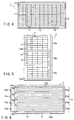
- FIG. 4 is a plan view schematically showing a module according to the second embodiment of the present invention.
- the module 1 shown in FIG. 4 is substantially equal in construction to the module 1 shown in FIG. 1, except that the module shown in FIG. 1 has a single series-connected array, whereas, the module shown in FIG. 4 has a plurality of series-connected arrays that are connected in parallel. Therefore, only the difference from the first embodiment will be described concerning the second embodiment.
- the cells 10 are connected in series in the vertical direction to form a plurality of series-connected arrays 11. These series-connected arrays 11 are connected in parallel by a pair of electrode bus bars 12 acting as common electrodes and each formed of a ribbon-like copper foil or the like.
- the output of the module 1 is not lowered so much as in a module having a single series-connected structure.
- each of the series-connected arrays 11 is designed to permit the short-circuit current not to exceed 600 mA under the conditions that a xenon lamp is used as a light source, the irradiance is set at 100 mW/cm 2 , A.M. (air mass) is set at 1.5, and the temperature is 25°C.
- the module 1 is not heated so much as to melt the metal back surface electrode layer 5 of the cell 10 even if the photoelectromotive force of any of the cells 10 is lowered to zero. Thus, the cell 10 is prevented from being broken.
- the short-circuit current of the series-connected array 11 under the conditions given above is not larger than 300 mA, preferably not larger than 200 mA. With decrease in the short-circuit current of the series-connected array 11, the cell 10 can be prevented from being broken more effectively.
- the above-noted effect produced by the second embodiment of the present invention is rendered particularly prominent under the conditions that the module 1 is heated to a high temperature when the hot spot phenomenon has taken place, i.e., in the case where the short-circuit current of the module 1 is large. It follows that the second embodiment is effective in the case where the short-circuit current of the module 1 under the conditions given above is not smaller than 1A, particularly, not smaller than 1.2A.
- the above-noted effect is rendered particularly prominent under the conditions in which the hot spot phenomenon is likely to be generated, i.e., in the case where the open-circuit voltage of the series-connected array 11 is high. Therefore, the second embodiment is advantageous in the case where the open-circuit voltage of the series-connected array 11 under the conditions given above is not lower than 10V or in the case where the series-connected array 11 consists of at least 12 cells 10.
- FIG. 5 is a plan view schematically showing the module 1 according to the third embodiment of the present invention.
- the module 1 shown in FIG. 5 comprises a plurality of series-connected arrays 11 that are connected in parallel as in the module 1 shown in FIG. 4.
- the module 1 in the third embodiment differs from the module 1 in the second embodiment in, for example, the shape of the common electrode 12. Only the difference from the second embodiment will be described concerning the third embodiment.
- the module 1 shown in FIG. 5 comprises mainly three regions 16a to 16c. In each of the regions 16a to 16c, a plurality of series-connected arrays 11 are connected in parallel by common electrodes 12a and 12b. Also, the common electrodes 12a and 12b are commonly used for all the regions 16a to 16c. In other words, in the module 1 shown in FIG. 5, all the series-connected arrays 11 included in regions 16a to 16c are connected in parallel.
- the number of cells 10 constituting each series-connected array 11 can be decreased without markedly changing the size of the cell 10, compared with the module shown in FIG. 4. Therefore, the module 1 shown in FIG. 5 is particularly useful in the case where a low voltage output is desired.
- FIG. 6 is a plan view schematically showing a module 1 according to the fourth embodiment of the present invention.
- the module 1 shown in FIG. 6, which is substantially equal in construction to the module 1 of the first embodiment shown in FIG. 1, differs from the module shown in FIG. 1 in that the module 1 shown in FIG. 5 comprises diodes 15a to 15d. Only the difference from the first embodiment will be described concerning the fourth embodiment shown in FIG. 6.
- the bus bar 12a is a cathode
- the bus bar 12b is an anode.
- the series-connected array 11 comprises four sub-arrays 13a to 13d that are connected in series.
- Each of the sub-arrays 13a to 13d comprises four cells 10 connected in series.
- the diodes 15a to 15d are connected in parallel in the forward direction relative to the power generation direction to the sub-arrays 13a to 13d with terminals 14a to 14d interposed therebetween, respectively.
- the cell 10 included in, for example, the sub-array 13b loses the photoelectromotive force so as to increase the resistance in the module 1 of the particular construction.
- the photoelectromotive force generated in the other sub-arrays 13a, 13c and 13c is bypassed by the diode 15b, making it possible to suppress the reduction in the output of the module 1 to a minimum level.
- each of the sub-arrays 13a to 13d is formed of an N s number of cells (four cells 10 in FIG. 6).
- the number N s is set to meet the relationship denoted by an inequality N s ⁇ Va/Vb + 1 , where V a represents the withstand voltage of each cell 10, and V b represents the open-circuit voltage of each cell under the conditions given below:
- the photoelectromotive force V c of the cell 10 is lower than the open-circuit voltage V b under the conditions given above. Also, the module 1 meets the relationship (N s -1) ⁇ V b ⁇ V a . It follows that, in the module 1 shown in FIG. 6, the cell 10 is prevented from being broken by the hot spot phenomenon.
- the number N s it is desirable for the number N s , the withstand voltage V a in the reversed direction, and the open-circuit voltage V b to meet the relationship denoted by an inequality V a /V b -1 ⁇ N s .
- the reduction in the output of the module 1 caused by the loss of the photoelectromotive force of a certain cell 10 can be most effectively suppressed in the case where the number N s is 1. In this case, however, a large number of diodes 15n are required, leading to cost elevation or to decrease in the effective power generating region.
- the terminals 14a to 14e can be formed by utilizing the layer forming the cell 10.
- the terminals 14a to 14e can be formed by forming the metal electrode layer, etc. used in the thin film photoelectric conversion cell 10 to cover not only the power generating region but also the outer region thereof, followed by laser-scribing the outer region of the metal electrode layer.
- the diodes 15a to 15d can be mounted to the terminals 14a to 14e by, for example, soldering.
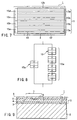
- FIG. 7 is a plan view schematically showing a module 7 according to the fifth embodiment.
- the module 1 shown in FIG. 7 is substantially equal in construction to the module 1 shown in FIG. 6, except that, in the module 1 shown in FIG. 7, the bypass diodes 15a to 15d are formed in the form of a thin film on the substrate, though the bypass diodes 15a to 15d are arranged outside the substrate in the module 1 shown in FIG. 6. Differences from the fourth embodiment alone are described concerning the fifth embodiment.
- each of these diodes 15a to 15d is of a laminate structure formed on the transparent substrate 2 and consisting of the transparent front surface electrode layer 3, the thin film photoelectric conversion unit 4 and the metal back surface electrode layer 5.
- FIG. 8 shows a circuit diagram showing the connection of the diode 15a to the sub-array 13a in the module 1 shown in FIG. 7.
- the diode 15a is connected in parallel in a forward direction relative to the power generating direction of the sub-array 13a
- the diode 15a and the sub-array 13a are opposite to each other in the direction of connection, as shown in FIG. 8.
- the transparent front surface electrode layer 3 of the diode 15a is electrically connected to the bus bar 12a or to the metal back surface electrode layer 5 adjacent to the bus bar 12a.
- the metal back surface electrode layer 5 of the diode 15a is electrically connected to the transparent front surface electrode layer 3 of the cell 10, which is positioned adjacent to the sub-array 13b, of the sub-array 13a or to the metal back surface electrode layer 5 of the cell 10, which is positioned adjacent to the sub-array 13a, of the sub-array 13b.
- the particular connection can be easily achieved by properly changing the laser scribing pattern of each layer.
- each of the diodes 15a to 15d has a construction similar to that of the cell 10. Also, the connection between the diodes 15a to 15d and the cells 10, etc. can be easily achieved by properly changing the laser scribing pattern of each layer. It follows that the module 1 shown in FIG. 7 can be manufactured easily, compared with the module 1 shown in FIG. 6.
- the diodes 15a to 15d are formed in a peripheral portion of the substrate 2.
- the module 1 is supported by a frame and, thus, the peripheral portion of the substrate 2 is not utilized for the power generation.
- the diodes 15a to 15d need not be irradiated with light.
- the diodes 15a to 15d it suffices for the diodes 15a to 15d to have a relatively small area. It follows that the surface of the substrate 2 can be effectively utilized by forming the diodes 15a to 15d in a peripheral region of the substrate 2.
- the diodes 15a to 15d are arranged in one edge portion of the substrate 2. However, these diodes can be arranged otherwise. For example, the diodes 15a to 15d can be alternately arranged on both edge portions of the substrate 2. Also, in each of the fourth and fifth embodiments, a single diode 15 is arranged for a single sub-array 13. Alternatively, a plurality of diodes may be arranged for a single sub-array. Further, in each of the fourth and fifth embodiments, the series-connected array 11 consists of four sub-arrays 13. However, it is also possible to employ another construction.
- FIG. 9 is a cross sectional view schematically showing a module 1 according to the sixth embodiment.
- the module 1 shown in FIG. 9, which is substantially equal in construction to the module of the first embodiment shown in FIGS. 1 and 2, differs from the module shown in FIGS. 1 and 2 in that a transparent oxide layer 6 is interposed between the thin film photoelectric conversion unit 4 and the metal back surface electrode layer 5, and a metal portion 8 is included in the module shown in FIG. 9. Only the differences from the first embodiment will be described concerning the sixth embodiment.
- the transparent oxide layer 6 has a hole or a groove formed in region 7, said hole or groove having the bottom surface constituted by the upper surface of the thin film photoelectric conversion unit 4. Also, a metal portion 8 made of a material constituting the metal back surface electrode layer 5 is formed in the hole or the groove. In other words, in the module 1 shown in FIG. 9, the hole or groove is filled with the material constituting the metal back surface electrode layer 5.
- the region 7 is sandwiched between the transparent front surface electrode layer 3 and the metal back surface electrode layer 5 and corresponds to a region to which an effective voltage is applied or applying a reversed bias voltage to the cell 10.
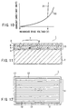
- FIG. 10 is a graph showing the electrical characteristics of the cell 10 included in the module 1 shown in FIG. 9.
- the reversed bias voltage applied to the cell 10 is plotted on the abscissa.
- the current flowing through the cell 10 immediately after application of the reversed bias voltage is plotted on the ordinate.
- Curve 20 shown in the graph covers the case where the metal portion 8 is not arranged, with curve 21 covering the case where the metal portion 8 is arranged.
- the current flowing through the cell immediately after application of the reversed bias voltage is small even if the applied reversed bias voltage exceeds a predetermined value, e.g., 8V, as denoted by curve 20.
- a predetermined value e.g. 8V
- the short-circuiting between the metal back surface electrode layer and the transparent front surface electrode layer does not take place promptly, since the cell must be heated to or higher than a temperature at which the transparent oxide layer is melted in order to bring about short-circuiting between the metal back surface electrode layer and the transparent front surface electrode layer.
- the metal portion 8 is arranged in the module 1, a very large current flows through the cell 10 immediately after the voltage application, if a predetermined reversed bias voltage, e.g., 8V, is applied to the cell 10, as denoted by curve 21.
- a predetermined reversed bias voltage e.g. 8V
- the transparent oxide layer 6 need not be melted for bringing about short-circuiting between the metal back surface electrode layer 5 and the transparent front surface electrode layer 3. It follows that the short-circuiting between them is brought about immediately after applying a predetermined reversed bias voltage.
- the short-circuiting between the metal portion 8 and the transparent front surface electrode layer 3 is not obstructed by the transparent oxide layer 6 when a predetermined reversed bias voltage is applied to the cell 10. Therefore, short-circuiting can be brought about immediately between the metal back surface electrode layer 5 and the transparent front surface electrode layer 3. In other words, when the light to one of the cells 10 is intercepted, the light-intercepted cell 10 is prevented from being heated excessively, leading to a high reliability of the module 1.
- the short-circuiting it is desirable for the short-circuiting to be brought about when a reversed bias voltage of at least 8V is applied to the cell 10.
- a reversed bias voltage it is possible for a reversed bias voltage to be applied to the cell 10 in an attempt to repair the defective portion of the cell 10.
- such a reversed bias treatment is carried out under voltage lower than 8V. Therefore, an undesired short-circuiting during the reversed bias treatment can be prevented by designing the module such that the short-circuiting takes place when a reversed bias voltage of at least 8V is applied to the module.
- the module 1 shown in FIG. 9 is designed in general such that the short-circuiting takes place immediately after application of a reversed bias voltage not higher than 10V to the module 1. In this case, the cell 10 is prevented from being heated to 200°C or more.
- the magnitude of the reversed bias voltage that can bring about the short-circuiting in question can be controlled by the size, number, etc. of the metal portions 8.
- 1 to 3 metal portions 8 are arranged in a single cell 10.
- the contact area between the metal portion 8 and the thin film photoelectric conversion unit 4 is designed to occupy preferably 0.1% to 10%, more preferably about 1%, of that portion of one surface of the thin film photoelectric conversion unit 4 which is positioned within region 7.
- the metal portion 8 and the metal back surface electrode layer 5 are made of the same material. Therefore, the metal portion 8 and the metal back surface electrode layer 5 can be formed simultaneously by forming the metal back surface electrode layer 5 after formation of a hole or groove corresponding to the metal portion 8 in the transparent oxide layer 6 by, for example, a laser scribing.
- FIG. 11 is a cross sectional view schematically showing the module 1 according to the seventh embodiment of the present invention.
- the module 1 of the seventh embodiment which is substantially equal in construction to the module 1 of the sixth embodiment shown in FIG. 9, differs from the module 1 of the sixth embodiment in that the metal portion 8 is formed on the transparent front surface electrode layer 3. Only the differences from the sixth embodiment will be described concerning the seventh embodiment.
- the module 1 shown in FIG. 11 is equal to that shown in FIG. 9 in that the short-circuiting between the metal portion 8 and the metal back surface electrode layer 5 is not obstructed by the transparent oxide layer 6 when a predetermined reversed bias voltage is applied to the cell 10. Therefore, short-circuiting between the metal back surface electrode layer 5 and the transparent front surface electrode 3 can be brought about promptly. In other words, when the light to one of the cells 10 is intercepted, the light-intercepted cell 10 is prevented from being heated excessively.
- the metal portion 8 and the metal back surface electrode layer 5 are formed as separate members of the module 1. Naturally, the metal portion 8 and the metal back surface electrode layer 5 can be made of materials differing from each other.
- the metal portion 8 is made of, for example, silver or aluminum.
- the metal back surface electrode layer 5 can be insulated again from the transparent front surface electrode layer 3 by applying a forward voltage to the cell 10. In other words, the cell 10, even if broken down, can be repaired easily.
- the metal portion 8 is in direct contact with the thin film photoelectric conversion unit 4.
- the metal portion 8 it is not absolutely necessary for the metal portion 8 to be brought into direct contact with the thin film photoelectric conversion unit 4.
- a conductive thin film having a melting point higher than that of the metal portion 8 is interposed between the metal portion 8 and the thin film photoelectric conversion unit 4, i.e., where the metal portion 8 is brought into indirect contact with the thin film photoelectric conversion unit 4 with the conductive thin film interposed therebetween
- the particular effect described above as far as the melting point of the conductive thin film is not higher than that of the transparent oxide layer 6 and the thickness of the conductive thin film is not larger than 50% of the thickness of the transparent oxide film 6, though the effect obtained is not so prominent as in the case of bringing the metal portion 8 into direct contact with the thin film photoelectric conversion unit 4.
- the first to seventh embodiments of the present invention measures are taken to suppress the behavior of the cell as a diode, to prevent a large current from flowing through the cell having the light thereto intercepted, or to facilitate the short-circuiting in the cell having the light thereto intercepted.
- the first to seventh embodiments of the present invention permit improving the reliability of the thin film photoelectric conversion module.
- a laminate structure consisting of the transparent electrode layer 3, the thin film photoelectric conversion unit 4 having a p-i-n junction, and the metal electrode layer 5 is formed on the transparent substrate 2 such that the transparent electrode layer 3 is in direct contact with the transparent substrate 2.
- the module of the present invention may be of another structure.
- a laminate structure consisting of a metal electrode layer, a thin film photoelectric conversion unit having an n-i-p junction and a transparent electrode layer may be formed on a substrate such that the metal electrode layer is in direct contact with the substrate. It is also possible for the thin film photoelectric conversion unit 4 to be of a tandem type.
- a thin film photoelectric conversion module as shown in FIGS. 1 and 2 was prepared as follows.
- an SnO 2 film 3 formed on one surface of the glass substrate 2 was scribed by laser scanning in parallel to the longer side of the substrate 1 by using a YAG laser so as to divide the SnO 2 film 3 into a plurality band-like patterns.
- a p-type hydrogen-containing amorphous silicon carbide layer 41 having a thickness of 10 nm, an i-type hydrogen-containing amorphous silicon layer 42 having a thickness of 300 nm and an n-type hydrogen-containing microcrystalline silicon layer 43 having a thickness of 10 nm were successively formed by a plasma CVD method on the SnO 2 film 3.
- the p-type hydrogen-containing silicon carbide layer 41 was doped with an impurity of boron.
- the i-type hydrogen-containing amorphous silicon layer was not doped with an impurity.
- the n-type hydrogen-containing microcrystalline silicon layer 43 was doped with phosphorus. In this fashion, the thin film photoelectric conversion unit 4 having a p-i-n junction was formed.
- the thin film photoelectric conversion unit 4 was scribed by laser scanning in parallel to the longer side of the substrate 1 by using a YAG laser so as to divide the thin film photoelectric conversion unit 4 into a plurality of band-like patterns.
- a back surface electrode layer was formed by successively forming a ZnO film (not shown) having a thickness of 100 nm and a Ag film 5 having a thickness of 300 nm on the thin film photoelectric conversion unit 4 by a sputtering method.
- the back surface electrode layer was also subjected to a laser-scribing by using a YAG laser so as to divide the back surface electrode layer into a plurality of band-like patterns.
- a series-connected array 11 consisting of 50 thin film photoelectric conversion cells 10 each sized at 10 mm ⁇ 800 mm, which were connected in series in a vertical direction, i.e., in a direction parallel to the shorter side of the substrate 2.
- a pair of electrode bus bars 12 were mounted to both edge portions of the series-connected array 11, followed by bringing a pair of conductor portions connected to a power source into contact with the Ag films 5 of the adjacent thin film photoelectric conversion cells 10 so as to apply voltage for 3 seconds in the direction of the power generation of the cell 10.
- the conductor portion noted above was shaped to conform with the thin film photoelectric conversion cell 10.
- the voltage applied to the cell 10 was what was obtained by superposing an AC voltage of 60 Hz on a DC voltage and, thus, the applied voltage was periodically changed within a range of between 0V and 9V.
- the module 1 shown in FIGS. 1 and 2 was obtained by applying the particular reversed bias treatment to all the cells 10.
- Ten modules 1 were prepared by the method described above, and the output characteristics of these modules were examined by a solar simulator with an irradiance of 100 mW/cm 2 using a xenon lamp as a light source and an air mass (A.M.) of 1.5.
- the measuring temperature was set at 25°C.
- the open-circuit voltage of the series-connected array 11 was found to be 42.5V
- the short circuit current was found to be 1A
- F.F. was found to be 70%.
- the open-circuit voltage of the thin film photoelectric conversion cells 10 under the conditions given above was 0.85V on the average, and each of the thin film photoelectric conversion cells 10 was capable of permitting current of the magnitude equal to the short-circuit current of the series-connected array 11 under the conditions given above to flow in a direction equal to the power generating direction upon application of a reversed bias voltage of 8V.
- each of these modules 1 was short-circuited and left to stand under the light irradiating conditions given above.
- the light to one of the cells 10 was intercepted to make zero the photoelectromotive force of the light-intercepted cell.
- each module 1 was inspected to see whether or not the cell 10 was broken. Breakage of the cell 10 was not recognized in any of all the modules 1. Also, the cell 10 having the light thereto intercepted was not heated excessively and the temperature thereof was not elevated to 200°C.
- Example 1 Ten modules were prepared as in Example 1, except that the reversed bias treatment was not performed. The output characteristics of these modules were also examined under the conditions equal to those employed in Example 1. The open-circuit voltage of the series-connected array was found to be 42.5V, the short-circuit current was found to be 1A, and F.F. was found to be 70%. Also, the open-circuit voltage of the thin film photoelectric conversion cell under the conditions given above was found to be 0.85V.
- each of these modules 1 was short-circuited and left to stand under the light irradiating conditions given above.
- the light to one of the cells 10 was intercepted to make zero the photoelectromotive force of the light-intercepted cell.
- each module 1 was inspected to see whether or not the cell 10 was broken. The cell 10 was found to have been broken in any all the modules 1. Also, the cell 10 having the light thereto intercepted was excessively heated to cause the temperature thereof to far exceed 200°C.
- the thin film photoelectric conversion module 1 constructed as shown in FIG. 4 was prepared as follows. Incidentally, the construction in cross section of the thin film photoelectric conversion module 1 shown in FIG. 4 is substantially equal to that of the module 1 shown in FIG. 1. Therefore, FIGS. 2 and 4 will be referred to in the following description of this Example.
- an SnO 2 film 3 formed on one main surface of the glass substrate 2 was scribed by the method similar to that employed in Example 1 to divide the SnO 2 film 3 into a plurality of band-like patterns, followed by forming a thin film photoelectric conversion unit 4.
- the thin film photoelectric conversion unit 4 was scribed by laser scanning in a direction parallel to the longer side of the substrate 1 by using a YAG laser so as to divide the thin film photoelectric conversion unit 4 into a plurality of band-like patterns.
- a back surface electrode layer was formed by successively forming by a sputtering method a ZnO film (not shown) having a thickness of 90 nm and an Ag film 5 having a thickness of 300 nm on the thin film photoelectric conversion unit 4.
- the back surface electrode layer was also subjected to a laser scribing by using a YAG laser so as to divide the back surface electrode layer into a plurality of band-like patterns.
- a laser scribing using a YAG laser was applied in a direction parallel to the shorter side of the substrate 2 so as to divide the SnO 2 film 3, the thin film photoelectric conversion unit 4 and the back surface electrode layer along the longer side of the substrate 2.
- 4 series-connected arrays 11 each consisting of 50 thin film photoelectric conversion cells 10 each sized at 10 mm ⁇ 200 mm and connected in series in the vertical direction (i.e., in a direction parallel to the shorter side of the substrate 2).
- a pair of electrode bus bars 12 were mounted to the substrate 2 to connect these series-connected arrays 11 in parallel.
- Tedler trade name of a fluorocarbon resin-series sheet, not shown
- Tedler was laminated on that surface of the substrate 2 on which the series-connected arrays 11 were formed, with an EVA layer (not shown) interposed between the series-connected arrays 11 and the fluorocarbon resin-series sheet, so as to obtain the module 1.
- Ten modules 1 were prepared by the method described above, and the output characteristics of these modules were examined under the conditions similar to those in Example 1. As a result, the open-circuit voltage of the series-connected array 11 was found to be 44V, the short circuit current was found to be 250 mA.
- each of these modules 1 was short-circuited and left to stand under the light irradiating conditions given above.
- the light to one of the cells 10 was intercepted to make zero the photoelectromotive force of the light-intercepted cell.
- each module 1 was inspected to see whether or not the cell 10 was broken. Breakage of the cell 10 was not recognized in any of all the modules 1. Also, the cell 10 having the light thereto intercepted was not heated excessively and the temperature thereof was not elevated to 200°C.
- Ten thin film photoelectric conversion modules were prepared as in Example 2, except that a laser-scribing in a direction parallel to the shorter side of the substrate was not applied and a single series-connected array, in which 50 thin film photoelectric conversion cells each sized at 10 mm ⁇ 800 mm were connected in series in the vertical direction, was formed.
- each of these modules 1 was short-circuited and left to stand under the light irradiating conditions given above.
- the light to one of the cells 10 was intercepted.
- each module 1 was inspected to see whether or not the cell 10 was broken. The cell 10 was found to have been broken in any all the 10 modules 1. Also, the cell 10 having the light thereto intercepted was excessively heated to cause the temperature thereof to far exceed 200°C.
- the thin film photoelectric conversion module 1 constructed as shown in FIG. 7 was prepared as follows. Incidentally, the construction in cross section of the thin film photoelectric conversion module 1 shown in FIG. 7 is substantially equal to that of the module 1 shown in FIG. 1. Therefore, FIGS. 2 and 7 will be referred to in the following description of this Example.
- an SnO 2 film 3 formed on one main surface of the glass substrate 2 was patterned to conform with the cells 10 and the diodes 15 by a laser-scribing using a YAG laser.
- the p-type hydrogen-containing amorphous silicon carbide layer 41 was doped with boron acting as a p-type impurity.
- the i-type hydrogen-containing amorphous silicon layer 42 was not doped with an impurity.
- the n-type hydrogen-containing microcrystalline silicon layer 43 was doped with phosphorus. In this fashion, a thin film photoelectric conversion unit 4 having a p-i-n junction was prepared.
- the thin film photoelectric conversion unit 4 was patterned to conform with the cells 10 and the diodes 15 by applying a laser-scribing using a YAG laser.
- a back surface electrode layer was formed by successively forming by a sputtering method a ZnO film (not shown) having a thickness of 100 nm and an Ag film 5 having a thickness of 300 nm on the thin film photoelectric conversion unit 4.
- the back surface electrode layer was also subjected to a laser scribing by using a YAG laser.
- the SnO 2 film 3, the thin film photoelectric conversion unit 4 and the back surface electrode layer were subjected to a laser scribing by using a YAG laser so as to insulate the power generating region from the peripheral region of the substrate.
- the series-connected array 11 consisting of 45 thin film photoelectric conversion cells 10 each sized at 10 mm ⁇ 900 mm and connected in series in the vertical direction, i.e., in a direction parallel to the shorter side of the substrate 2, and 5 diodes 15 each sized at 90 mm ⁇ 2 mm.
- these 5 diodes 15 were respectively connected in parallel to 5 groups of cells 10, each group consisting of 9 cells connected in series, in a forward direction relative to the power generation direction.
- a pair of electrode bus bars 12a and 12b were mounted to both edge portions of the series-connected array 11.
- Tedler trade name of a fluorocarbon resin-series sheet, not shown
- Tedler was laminated on that surface of the substrate 2 on which the series-connected arrays 11 were formed, with an EVA layer (not shown) interposed between the series-connected arrays 11 and the fluorocarbon resin-series sheet, so as to obtain the module 1.
- Ten modules 1 were prepared by the method described above, and the output characteristics of these modules were examined under the conditions similar to those in Example 1. As a result, the open-circuit voltage of the series-connected array 11 was found to be 40V, and the short circuit current was found to be 1.3A. Also, the withstand voltage of each cell 10 of these modules 1 was measured before lamination of the EVA layer and the fluorocarbon-series sheet. The withstand voltage was found to be 8V on the average.
- each of these modules 1 was short-circuited and left to stand under the light irradiating conditions given above.
- the light to one of the cells 10 was intercepted by attaching a black vinyl tape to the light-receiving surface of the cell 10 to make zero the photoelectromotive force of the light-intercepted cell.
- each module 1 was inspected to see whether or not the cell 10 was broken. Breakage of the cell 10 was not recognized in any of all the modules 1. Also, the cell 10 having the light thereto intercepted was not heated excessively and the temperature thereof was not elevated to 200°C.
- Example 3 Ten thin film photoelectric conversion modules were prepared as in Example 3, except that the series-connected array consisting of 45 thin film photoelectric conversion cells each sized at 10 mm ⁇ 900 mm and connected in series in the vertical direction was formed without forming the diodes 15.
- the output characteristics of these modules were also examined under the conditions equal to those in Example 3.
- the open-circuit voltage of the module was found to be 40V and the short-circuit current was found to be 1.3A. Also, the withstand voltage in the reverse direction of each cell was found to be 8V on the average.
- each of these modules was short-circuited and left to stand under the light irradiating conditions given above.
- the light to one of the cells was intercepted by attaching a black vinyl tape to the light-receiving surface of the cell 10 to make zero the photoelectromotive force of the light-intercepted cell.
- each module was inspected to see whether or not the cell was broken. Breakage of the cell was recognized any of all the modules. Also, the cell having the light thereto intercepted was heated to far exceed 200°C.
- FIG. 12 is a plan view schematically showing a thin film photoelectric conversion module 1 prepared in this Example.
- the module 1 shown in FIG. 12 was substantially equal in construction to the module 1 shown in FIG. 9, except the shape of the metal portion 8. Therefore, FIGS. 9 and 12 will be referred to in describing the method of manufacturing the module 1 shown in FIG. 12.
- an SnO 2 film 3 formed on one main surface of the glass substrate 2 was subjected to a laser scanning by using a YAG laser in a direction parallel to the longer side of the substrate 1 so as to divide the SnO 2 film 3 into a plurality of band-like patterns.
- a p-type hydrogen-containing amorphous silicon carbide layer having a thickness of 10 nm an i-type hydrogen containing amorphous silicon layer having a thickness of 300 nm, and an n-type hydrogen-containing microcrystalline silicon layer having a thickness of 10 nm.
- the p-type hydrogen-containing amorphous silicon carbide layer was doped with an impurity of boron.
- the i-type hydrogen-containing amorphous silicon layer was not doped with an impurity.
- the n-type hydrogen-containing microcrystalline silicon layer was doped with phosphorus. In this fashion, obtained was a thin film photoelectric conversion unit 4 having a p-i-n junction.
- the thin film photoelectric conversion unit 4 was scribed by applying a laser scanning using a YAG laser in a direction parallel to the longer side of the substrate 1 so as to divide the thin film photoelectric conversion unit 4 into a plurality of band-like patterns.
- a ZnO film 5 having a thickness of 100 nm was formed by a sputtering method on the thin film photoelectric conversion unit 4.
- a mask was used such that the ZnO film 5 was not formed in a peripheral region, 2 mm wide, at one edge of the plural band-like patterns.
- the ZnO film 5 was formed to provide a non-film forming region 17 sized at 10 mm ⁇ 2 mm at one edge of the plural band-like patterns.
- a Ag film 6 was formed by a sputtering method in a thickness of 300 nm on the ZnO film 5 and the non-film forming region 17.
- the Ag film 6 formed on the non-film forming region 17 performs the function of the metal portion 8.
- These ZnO film 5 and the Ag film 6 were also subjected to a laser scribing by using a YAG laser so as to be divided into a plurality of band-like patterns.
- a series-connected array 11 consisting of 50 thin film photoelectric conversion cells 10 each sized at 10 mm ⁇ 800 mm and connected in series in the vertical direction (i.e., in a direction parallel to the shorter side of the substrate 2.
- this series-connected array 11 a single metal portion 8 is arranged in each cell 10. Also, the area of the region 7 shown in FIG. 9 was 76 cm 2 .
- Ten modules 1 were prepared by the method described above, and the output characteristics of these modules were examined under the conditions equal to those in Example 1.
- the open-circuit voltage of the series-connected array 11 was found to be 43V, and the short-circuit current was found to be 1A.
- each of these modules 1 was short-circuited to observe the changes in the output current under the illuminating conditions given above.
- the light to one of the cells 10 was intercepted so as to make zero the photoelectromotive force of the light-intercepted cell.
- a reversed bias voltage of 42V was applied to the light-intercepted cell 10.
- the time from the initiation of the light irradiation to the point at which the output current was markedly increased was measured on the basis that the SnO 2 film 3 and the Ag film 6 were short-circuited when the output current was markedly increased.
- the output current of the module 1 was found to have reached 1A immediately after initiation of the light irradiation and to have remained constant thereafter.
- the light-intercepted cell was not heated excessively, and the temperature thereof did not reach 200°C.
- Example 4 Ten modules were prepared as in Example 4, except that the module did not include the metal portion 8. To be more specific, 10 modules were prepared as in Example 4, except that the ZnO film was formed without forming the non-film forming region 17 for the metal portion 8.
- each of these modules was short-circuited to observe the changes in the output current under the illuminating conditions given above.
- the light to one of the cells was intercepted so as to make zero the photoelectromotive force of the light-intercepted cell.
- a reversed bias voltage of 42V was applied to the light-intercepted cell.
- the time from the initiation of the light irradiation to the point at which the output current was markedly increased was measured on the basis that the SnO 2 film 3 and the Ag film 6 were short-circuited when the output current was markedly increased.
- the output current of the module was found to have rapidly increased one second after initiation of the light irradiation, finally reaching 1A. Also, the light-intercepted cell was heated excessively to cause the temperature thereof far to exceed 200°C.
- the present invention provides a thin film photoelectric conversion module having a high reliability and a method of manufacturing the same.
Priority Applications (2)
| Application Number | Priority Date | Filing Date | Title |
|---|---|---|---|
| EP10175900A EP2256824A3 (fr) | 1999-08-25 | 2000-03-01 | Module de conversion photoélectrique en couche mince et son procédé de fabrication |
| EP14184222.9A EP2835834A3 (fr) | 1999-08-25 | 2000-03-01 | Module de conversion photoélectrique à couche mince et son procédé de fabrication |
Applications Claiming Priority (8)
| Application Number | Priority Date | Filing Date | Title |
|---|---|---|---|
| JP23870999A JP2001068696A (ja) | 1999-08-25 | 1999-08-25 | 薄膜光電変換モジュール |
| JP23870999 | 1999-08-25 | ||
| JP23870899A JP4053193B2 (ja) | 1999-08-25 | 1999-08-25 | 薄膜光電変換モジュール |
| JP23870899 | 1999-08-25 | ||
| JP26221599 | 1999-09-16 | ||
| JP26221499 | 1999-09-16 | ||
| JP26221599A JP3246732B2 (ja) | 1999-09-16 | 1999-09-16 | 薄膜光電変換モジュール及びその製造方法 |
| JP26221499A JP2001085709A (ja) | 1999-09-16 | 1999-09-16 | 薄膜光電変換モジュール |
Related Child Applications (1)
| Application Number | Title | Priority Date | Filing Date |
|---|---|---|---|
| EP14184222.9A Division EP2835834A3 (fr) | 1999-08-25 | 2000-03-01 | Module de conversion photoélectrique à couche mince et son procédé de fabrication |
Publications (2)
| Publication Number | Publication Date |
|---|---|
| EP1079441A2 true EP1079441A2 (fr) | 2001-02-28 |
| EP1079441A3 EP1079441A3 (fr) | 2007-12-26 |
Family
ID=27477741
Family Applications (3)
| Application Number | Title | Priority Date | Filing Date |
|---|---|---|---|
| EP14184222.9A Withdrawn EP2835834A3 (fr) | 1999-08-25 | 2000-03-01 | Module de conversion photoélectrique à couche mince et son procédé de fabrication |
| EP00103474A Ceased EP1079441A3 (fr) | 1999-08-25 | 2000-03-01 | Module de conversion photoélectrique en couche mince et son procédé de fabrication |
| EP10175900A Withdrawn EP2256824A3 (fr) | 1999-08-25 | 2000-03-01 | Module de conversion photoélectrique en couche mince et son procédé de fabrication |
Family Applications Before (1)
| Application Number | Title | Priority Date | Filing Date |
|---|---|---|---|
| EP14184222.9A Withdrawn EP2835834A3 (fr) | 1999-08-25 | 2000-03-01 | Module de conversion photoélectrique à couche mince et son procédé de fabrication |
Family Applications After (1)
| Application Number | Title | Priority Date | Filing Date |
|---|---|---|---|
| EP10175900A Withdrawn EP2256824A3 (fr) | 1999-08-25 | 2000-03-01 | Module de conversion photoélectrique en couche mince et son procédé de fabrication |
Country Status (3)
| Country | Link |
|---|---|
| US (1) | US6288323B1 (fr) |
| EP (3) | EP2835834A3 (fr) |
| AU (1) | AU767581B2 (fr) |
Cited By (7)
| Publication number | Priority date | Publication date | Assignee | Title |
|---|---|---|---|---|
| FR2863775A1 (fr) * | 2003-12-15 | 2005-06-17 | Photowatt Internat Sa | Module photovoltaique avec un dispositif electronique dans l'empilage lamine. |
| WO2007118814A2 (fr) * | 2006-04-13 | 2007-10-25 | Shell Erneuerbare Energien Gmbh | Module solaire |
| EP1930948A1 (fr) | 2006-12-06 | 2008-06-11 | SCHOTT Solar GmbH | Configuration des éléctrodes pour un panneau photovoltaïque avec des cellules connectées en série |
| EP2184789A1 (fr) * | 2007-08-06 | 2010-05-12 | Sharp Kabushiki Kaisha | Procédé et appareil de fabrication d'un module de conversion photoélectrique en couches minces |
| CN101421846B (zh) * | 2006-04-13 | 2011-06-15 | 壳牌可再生能源有限公司 | 太阳能电池组件 |
| WO2012026822A1 (fr) * | 2010-08-26 | 2012-03-01 | Innotech Solar Asa | Module photovoltaïque avec diodes de cellules solaires intégrées |
| EP2169729A4 (fr) * | 2007-07-13 | 2015-11-18 | Sharp Kk | Module de pile solaire en couche mince |
Families Citing this family (45)
| Publication number | Priority date | Publication date | Assignee | Title |
|---|---|---|---|---|
| US20140102502A1 (en) * | 2006-04-13 | 2014-04-17 | Daniel Luch | Collector grid and interconnect structures for photovoltaic arrays and modules |
| US6423595B1 (en) * | 2001-04-19 | 2002-07-23 | United Solar Systems Corporation | Method for scribing a semiconductor device |
| JP2003069055A (ja) * | 2001-06-13 | 2003-03-07 | Sharp Corp | 太陽電池セルとその製造方法 |
| JP2004096079A (ja) * | 2002-07-11 | 2004-03-25 | Sharp Corp | 光電変換装置、画像読取装置および光電変換装置の製造方法 |
| JP2004127987A (ja) * | 2002-09-30 | 2004-04-22 | Sharp Corp | 太陽電池セルおよびその製造方法 |
| US7339110B1 (en) * | 2003-04-10 | 2008-03-04 | Sunpower Corporation | Solar cell and method of manufacture |
| US9865758B2 (en) | 2006-04-13 | 2018-01-09 | Daniel Luch | Collector grid and interconnect structures for photovoltaic arrays and modules |
| KR20080021428A (ko) * | 2006-09-04 | 2008-03-07 | 엘지전자 주식회사 | 바이패스 다이오드를 포함하는 광기전력 변환장치 및 그제조방법 |
| US20080128018A1 (en) * | 2006-12-04 | 2008-06-05 | Richard Allen Hayes | Solar cells which include the use of certain poly(vinyl butyral)/film bilayer encapsulant layers with a low blocking tendency and a simplified process to produce thereof |
| US8197928B2 (en) | 2006-12-29 | 2012-06-12 | E. I. Du Pont De Nemours And Company | Intrusion resistant safety glazings and solar cell modules |
| US7943845B2 (en) * | 2007-02-07 | 2011-05-17 | E. I. Du Pont De Nemours And Company | Solar cells encapsulated with poly(vinyl butyral) |
| WO2009104601A1 (fr) * | 2008-02-18 | 2009-08-27 | シャープ株式会社 | Module de cellule solaire à couche mince |
| US20110011439A1 (en) * | 2008-02-25 | 2011-01-20 | Masatomo Hasegawa | Photovoltaic power system |
| US20090229596A1 (en) | 2008-03-12 | 2009-09-17 | Myung-Hun Shin | Solar energy module having repair line, solar energy assembly having the same, method of repairing the solar energy module and method of trimming the solar energy assembly |
| BRPI0907078A2 (pt) * | 2008-03-26 | 2015-07-07 | Du Pont | "artigo laminado" |
| JP2011517096A (ja) * | 2008-04-04 | 2011-05-26 | イー・アイ・デュポン・ドウ・ヌムール・アンド・カンパニー | 高メルトフローのポリ(ビニルブチラール)封止材を含む太陽電池モジュール |
| US20090288701A1 (en) * | 2008-05-23 | 2009-11-26 | E.I.Du Pont De Nemours And Company | Solar cell laminates having colored multi-layer encapsulant sheets |
| CN102113125B (zh) * | 2008-08-08 | 2013-06-05 | 京半导体股份有限公司 | 采光型太阳电池模组 |
| CA2731990C (fr) * | 2008-08-08 | 2016-08-02 | Kyosemi Corporation | Module de batteries solaires pour eclairage naturel |
| JP5376873B2 (ja) * | 2008-09-03 | 2013-12-25 | シャープ株式会社 | 集積型薄膜太陽電池 |
| JP5171490B2 (ja) * | 2008-09-04 | 2013-03-27 | シャープ株式会社 | 集積型薄膜太陽電池 |
| JP2010074071A (ja) * | 2008-09-22 | 2010-04-02 | Sharp Corp | 集積型薄膜太陽電池およびその製造方法 |
| US8071420B2 (en) * | 2008-12-19 | 2011-12-06 | Applied Materials, Inc. | Edge film removal process for thin film solar cell applications |
| JP4637244B2 (ja) * | 2009-01-09 | 2011-02-23 | シャープ株式会社 | 薄膜太陽電池モジュール |
| IT1392995B1 (it) * | 2009-02-12 | 2012-04-02 | St Microelectronics Srl | Pannello solare con due moduli fotovoltaici multicellulari monolitici di diversa tecnologia |
| US20100132759A1 (en) * | 2009-06-12 | 2010-06-03 | Renhe Jia | Cell isolation on photovoltaic modules for hot spot reduction |
| KR101072073B1 (ko) * | 2009-06-30 | 2011-10-10 | 엘지이노텍 주식회사 | 태양광 발전장치 |
| US20110005458A1 (en) * | 2009-07-13 | 2011-01-13 | Applied Materials, Inc. | Method and apparatus for improving scribe accuracy in solar cell modules |
| US20110008947A1 (en) * | 2009-07-13 | 2011-01-13 | Applied Materials, Inc. | Apparatus and method for performing multifunction laser processes |
| DE102009042093A1 (de) * | 2009-09-18 | 2011-03-24 | Inventux Technologies Ag | Niederspannungsmodul mit Rückkontakt |
| KR20110032939A (ko) * | 2009-09-24 | 2011-03-30 | 삼성전자주식회사 | 태양 전지 및 그 제조 방법 |
| US20110272000A1 (en) * | 2010-05-06 | 2011-11-10 | Thermoguide Ltd. | Linear low concentration photovoltaic generator |
| US20110315184A1 (en) * | 2010-06-29 | 2011-12-29 | Primestar Solar, Inc. | Photovoltaic (pv) module with improved bus tape to foil ribbon contact |
| WO2013028591A2 (fr) * | 2011-08-22 | 2013-02-28 | Adhesives Research, Inc. | Ruban de barre omnibus revêtu polymère pour des systèmes photovoltaïques |
| US9219171B2 (en) | 2012-10-16 | 2015-12-22 | Solexel, Inc. | Systems and methods for monolithically integrated bypass switches in photovoltaic solar cells and modules |
| US9515217B2 (en) | 2012-11-05 | 2016-12-06 | Solexel, Inc. | Monolithically isled back contact back junction solar cells |
| USD1009775S1 (en) | 2014-10-15 | 2024-01-02 | Maxeon Solar Pte. Ltd. | Solar panel |
| USD933584S1 (en) | 2012-11-08 | 2021-10-19 | Sunpower Corporation | Solar panel |
| CN103117315A (zh) * | 2013-03-05 | 2013-05-22 | 天津英利新能源有限公司 | 太阳能电池片组、光伏组件及制造太阳能电池片的方法 |
| USD913210S1 (en) | 2014-10-15 | 2021-03-16 | Sunpower Corporation | Solar panel |
| USD999723S1 (en) | 2014-10-15 | 2023-09-26 | Sunpower Corporation | Solar panel |
| USD896747S1 (en) | 2014-10-15 | 2020-09-22 | Sunpower Corporation | Solar panel |
| USD933585S1 (en) | 2014-10-15 | 2021-10-19 | Sunpower Corporation | Solar panel |
| CN111640812B (zh) * | 2017-12-30 | 2023-02-28 | 苏州阿特斯阳光电力科技有限公司 | 光伏组件 |
| US10490682B2 (en) | 2018-03-14 | 2019-11-26 | National Mechanical Group Corp. | Frame-less encapsulated photo-voltaic solar panel supporting solar cell modules encapsulated within multiple layers of optically-transparent epoxy-resin materials |
Citations (6)
| Publication number | Priority date | Publication date | Assignee | Title |
|---|---|---|---|---|
| US4401839A (en) * | 1981-12-15 | 1983-08-30 | Atlantic Richfield Company | Solar panel with hardened foil back layer |
| US4514579A (en) * | 1984-01-30 | 1985-04-30 | Energy Conversion Devices, Inc. | Large area photovoltaic cell and method for producing same |
| JPS60218882A (ja) * | 1984-04-13 | 1985-11-01 | Mitsubishi Electric Corp | 光発電素子 |
| US5415579A (en) | 1991-04-24 | 1995-05-16 | Concepts Development Australia Pty Ltd | Doll with pivoting eyeballs, heart beat, voice means, burping sounds and actuating transmitter |
| JPH0964397A (ja) * | 1995-08-29 | 1997-03-07 | Canon Inc | 太陽電池および太陽電池モジュール |
| JPH11112010A (ja) * | 1997-10-08 | 1999-04-23 | Sharp Corp | 太陽電池およびその製造方法 |
Family Cites Families (12)
| Publication number | Priority date | Publication date | Assignee | Title |
|---|---|---|---|---|
| US4315096A (en) * | 1980-07-25 | 1982-02-09 | Eastman Kodak Company | Integrated array of photovoltaic cells having minimized shorting losses |
| EP0106854A1 (fr) * | 1982-04-27 | 1984-05-02 | The Australian National University | Reseaux d'elements polarises produisant de l'energie |
| US4754544A (en) * | 1985-01-30 | 1988-07-05 | Energy Conversion Devices, Inc. | Extremely lightweight, flexible semiconductor device arrays |
| AU583423B2 (en) * | 1985-09-21 | 1989-04-27 | Semiconductor Energy Laboratory Co. Ltd. | Semiconductor device free from the electrical shortage through a semiconductor layer and method for manufacturing same |
| US4749454A (en) * | 1986-11-17 | 1988-06-07 | Solarex Corporation | Method of removing electrical shorts and shunts from a thin-film semiconductor device |
| CA2024662A1 (fr) * | 1989-09-08 | 1991-03-09 | Robert Oswald | Module photovoltaique monolithique a elements montes en serie et en parallele |
| WO1992007386A1 (fr) * | 1990-10-15 | 1992-04-30 | United Solar Systems Corporation | Configuration monolithique de cellules solaires et methode de realisation |
| JP2837296B2 (ja) * | 1991-10-17 | 1998-12-14 | シャープ株式会社 | 太陽電池 |
| JP3202536B2 (ja) | 1994-07-19 | 2001-08-27 | シャープ株式会社 | バイパス機能付太陽電池セル |
| JP3653800B2 (ja) * | 1995-06-15 | 2005-06-02 | 株式会社カネカ | 集積化薄膜太陽電池の製造方法 |
| JP3740618B2 (ja) | 1996-06-17 | 2006-02-01 | 株式会社カネカ | 太陽電池の短絡部除去方法及び該短絡部除去装置 |
| JP3510740B2 (ja) * | 1996-08-26 | 2004-03-29 | シャープ株式会社 | 集積型薄膜太陽電池の製造方法 |
-
2000
- 2000-03-01 AU AU20613/00A patent/AU767581B2/en not_active Expired
- 2000-03-01 EP EP14184222.9A patent/EP2835834A3/fr not_active Withdrawn
- 2000-03-01 EP EP00103474A patent/EP1079441A3/fr not_active Ceased
- 2000-03-01 EP EP10175900A patent/EP2256824A3/fr not_active Withdrawn
- 2000-03-02 US US09/517,218 patent/US6288323B1/en not_active Expired - Lifetime
Patent Citations (7)
| Publication number | Priority date | Publication date | Assignee | Title |
|---|---|---|---|---|
| US4401839A (en) * | 1981-12-15 | 1983-08-30 | Atlantic Richfield Company | Solar panel with hardened foil back layer |
| US4514579A (en) * | 1984-01-30 | 1985-04-30 | Energy Conversion Devices, Inc. | Large area photovoltaic cell and method for producing same |
| JPS60182178A (ja) * | 1984-01-30 | 1985-09-17 | エナージー・コンバーション・デバイセス・インコーポレーテッド | 大面積光起電力電池とその製法 |
| JPS60218882A (ja) * | 1984-04-13 | 1985-11-01 | Mitsubishi Electric Corp | 光発電素子 |
| US5415579A (en) | 1991-04-24 | 1995-05-16 | Concepts Development Australia Pty Ltd | Doll with pivoting eyeballs, heart beat, voice means, burping sounds and actuating transmitter |
| JPH0964397A (ja) * | 1995-08-29 | 1997-03-07 | Canon Inc | 太陽電池および太陽電池モジュール |
| JPH11112010A (ja) * | 1997-10-08 | 1999-04-23 | Sharp Corp | 太陽電池およびその製造方法 |
Non-Patent Citations (4)
Cited By (11)
| Publication number | Priority date | Publication date | Assignee | Title |
|---|---|---|---|---|
| FR2863775A1 (fr) * | 2003-12-15 | 2005-06-17 | Photowatt Internat Sa | Module photovoltaique avec un dispositif electronique dans l'empilage lamine. |
| EP1544922A1 (fr) * | 2003-12-15 | 2005-06-22 | Photowatt International S.A. | Module photovoltaique avec un dispositif électronique dans l'empilage laminé |
| WO2007118814A2 (fr) * | 2006-04-13 | 2007-10-25 | Shell Erneuerbare Energien Gmbh | Module solaire |
| WO2007118814A3 (fr) * | 2006-04-13 | 2007-11-29 | Shell Erneuerbare En Gmbh | Module solaire |
| CN101421846B (zh) * | 2006-04-13 | 2011-06-15 | 壳牌可再生能源有限公司 | 太阳能电池组件 |
| EP1930948A1 (fr) | 2006-12-06 | 2008-06-11 | SCHOTT Solar GmbH | Configuration des éléctrodes pour un panneau photovoltaïque avec des cellules connectées en série |
| EP2169729A4 (fr) * | 2007-07-13 | 2015-11-18 | Sharp Kk | Module de pile solaire en couche mince |
| EP2184789A1 (fr) * | 2007-08-06 | 2010-05-12 | Sharp Kabushiki Kaisha | Procédé et appareil de fabrication d'un module de conversion photoélectrique en couches minces |
| EP2184789A4 (fr) * | 2007-08-06 | 2011-07-27 | Sharp Kk | Procédé et appareil de fabrication d'un module de conversion photoélectrique en couches minces |
| US8349623B2 (en) | 2007-08-06 | 2013-01-08 | Sharp Kabushiki Kaisha | Method and apparatus for manufacturing thin film photoelectric conversion module |
| WO2012026822A1 (fr) * | 2010-08-26 | 2012-03-01 | Innotech Solar Asa | Module photovoltaïque avec diodes de cellules solaires intégrées |
Also Published As
| Publication number | Publication date |
|---|---|
| AU767581B2 (en) | 2003-11-20 |
| EP2256824A2 (fr) | 2010-12-01 |
| EP1079441A3 (fr) | 2007-12-26 |
| AU2061300A (en) | 2001-03-01 |
| EP2256824A3 (fr) | 2012-09-12 |
| EP2835834A2 (fr) | 2015-02-11 |
| EP2835834A3 (fr) | 2015-06-10 |
| US6288323B1 (en) | 2001-09-11 |
Similar Documents
| Publication | Publication Date | Title |
|---|---|---|
| US6288323B1 (en) | Thin film photoelectric conversion module and method of manufacturing the same | |
| EP1258925B1 (fr) | Module de conversion photoélectrique en couche mince integré | |
| EP0631328B1 (fr) | Module de cellules solaires comportant une partie soudée à chaud pour améliorer la résistance à l'humidité | |
| US6784361B2 (en) | Amorphous silicon photovoltaic devices | |
| US8563347B2 (en) | Method for producing a thin-film photovoltaic cell having an etchant-resistant electrode and an integrated bypass diode and a panel incorporating the same | |
| JP4053193B2 (ja) | 薄膜光電変換モジュール | |
| US20100263719A1 (en) | Thin-Film Solar Cell Module | |
| US20120062035A1 (en) | Photovoltaic Device And Manufacturing Method | |
| JP2002373997A (ja) | 集積型ハイブリッド薄膜光電変換モジュール | |
| US20090308429A1 (en) | Thin-film solar module | |
| JPH06318723A (ja) | 光起電力素子およびその作製方法 | |
| US20120295395A1 (en) | Method for producing an array of thin-film photovoltaic cells having a totally separated integrated bypass diode associated with a plurality of cells and method for producing a panel incorporating the same | |
| KR20200048864A (ko) | 고출력 슁글드 어레이 구조의 태양전지 모듈 및 그 제조방법 | |
| JP2001068696A (ja) | 薄膜光電変換モジュール | |
| JP3246732B2 (ja) | 薄膜光電変換モジュール及びその製造方法 | |
| JP4272320B2 (ja) | 薄膜光電変換モジュールの欠陥修復方法及び薄膜光電変換モジュールの製造方法 | |
| JP4308387B2 (ja) | 薄膜光電変換モジュールの欠陥修復方法及び薄膜光電変換モジュールの製造方法 | |
| JP2001085709A (ja) | 薄膜光電変換モジュール | |
| Vijh | Triple junction amorphous silicon based flexible photovoltaic submodules on polyimide substrates | |
| JPH06318721A (ja) | 太陽電池 | |
| KR20180055542A (ko) | 태양 전지 패널 및 이의 제조 방법 |
Legal Events
| Date | Code | Title | Description |
|---|---|---|---|
| PUAI | Public reference made under article 153(3) epc to a published international application that has entered the european phase |
Free format text: ORIGINAL CODE: 0009012 |
|
| AK | Designated contracting states |
Kind code of ref document: A2 Designated state(s): AT BE CH CY DE DK ES FI FR GB GR IE IT LI LU MC NL PT SE |
|
| AX | Request for extension of the european patent |
Free format text: AL;LT;LV;MK;RO;SI |
|
| PUAL | Search report despatched |
Free format text: ORIGINAL CODE: 0009013 |
|
| AK | Designated contracting states |
Kind code of ref document: A3 Designated state(s): AT BE CH CY DE DK ES FI FR GB GR IE IT LI LU MC NL PT SE |
|
| AX | Request for extension of the european patent |
Extension state: AL LT LV MK RO SI |
|
| TPAC | Observations filed by third parties |
Free format text: ORIGINAL CODE: EPIDOSNTIPA |
|
| 17P | Request for examination filed |
Effective date: 20080328 |
|
| AKX | Designation fees paid |
Designated state(s): AT BE CH CY DE DK ES FI FR GB GR IE IT LI LU MC NL PT SE |
|
| 17Q | First examination report despatched |
Effective date: 20081023 |
|
| APBK | Appeal reference recorded |
Free format text: ORIGINAL CODE: EPIDOSNREFNE |
|
| APBN | Date of receipt of notice of appeal recorded |
Free format text: ORIGINAL CODE: EPIDOSNNOA2E |
|
| APBR | Date of receipt of statement of grounds of appeal recorded |
Free format text: ORIGINAL CODE: EPIDOSNNOA3E |
|
| APAF | Appeal reference modified |
Free format text: ORIGINAL CODE: EPIDOSCREFNE |
|
| RAP1 | Party data changed (applicant data changed or rights of an application transferred) |
Owner name: KANEKA CORPORATION |
|
| APBT | Appeal procedure closed |
Free format text: ORIGINAL CODE: EPIDOSNNOA9E |
|
| STAA | Information on the status of an ep patent application or granted ep patent |
Free format text: STATUS: THE APPLICATION HAS BEEN REFUSED |
|
| 18R | Application refused |
Effective date: 20140617 |