EP1079357A1 - Display panel - Google Patents
Display panel Download PDFInfo
- Publication number
- EP1079357A1 EP1079357A1 EP00904058A EP00904058A EP1079357A1 EP 1079357 A1 EP1079357 A1 EP 1079357A1 EP 00904058 A EP00904058 A EP 00904058A EP 00904058 A EP00904058 A EP 00904058A EP 1079357 A1 EP1079357 A1 EP 1079357A1
- Authority
- EP
- European Patent Office
- Prior art keywords
- printed circuit
- circuit board
- display panel
- disposed
- lines
- Prior art date
- Legal status (The legal status is an assumption and is not a legal conclusion. Google has not performed a legal analysis and makes no representation as to the accuracy of the status listed.)
- Withdrawn
Links
Images


Classifications
-
- G—PHYSICS
- G02—OPTICS
- G02F—OPTICAL DEVICES OR ARRANGEMENTS FOR THE CONTROL OF LIGHT BY MODIFICATION OF THE OPTICAL PROPERTIES OF THE MEDIA OF THE ELEMENTS INVOLVED THEREIN; NON-LINEAR OPTICS; FREQUENCY-CHANGING OF LIGHT; OPTICAL LOGIC ELEMENTS; OPTICAL ANALOGUE/DIGITAL CONVERTERS
- G02F1/00—Devices or arrangements for the control of the intensity, colour, phase, polarisation or direction of light arriving from an independent light source, e.g. switching, gating or modulating; Non-linear optics
- G02F1/01—Devices or arrangements for the control of the intensity, colour, phase, polarisation or direction of light arriving from an independent light source, e.g. switching, gating or modulating; Non-linear optics for the control of the intensity, phase, polarisation or colour
- G02F1/13—Devices or arrangements for the control of the intensity, colour, phase, polarisation or direction of light arriving from an independent light source, e.g. switching, gating or modulating; Non-linear optics for the control of the intensity, phase, polarisation or colour based on liquid crystals, e.g. single liquid crystal display cells
- G02F1/133—Constructional arrangements; Operation of liquid crystal cells; Circuit arrangements
-
- H—ELECTRICITY
- H05—ELECTRIC TECHNIQUES NOT OTHERWISE PROVIDED FOR
- H05K—PRINTED CIRCUITS; CASINGS OR CONSTRUCTIONAL DETAILS OF ELECTRIC APPARATUS; MANUFACTURE OF ASSEMBLAGES OF ELECTRICAL COMPONENTS
- H05K1/00—Printed circuits
- H05K1/18—Printed circuits structurally associated with non-printed electric components
- H05K1/182—Printed circuits structurally associated with non-printed electric components associated with components mounted in printed circuit boards [PCB], e.g. insert-mounted components [IMC]
-
- G—PHYSICS
- G02—OPTICS
- G02F—OPTICAL DEVICES OR ARRANGEMENTS FOR THE CONTROL OF LIGHT BY MODIFICATION OF THE OPTICAL PROPERTIES OF THE MEDIA OF THE ELEMENTS INVOLVED THEREIN; NON-LINEAR OPTICS; FREQUENCY-CHANGING OF LIGHT; OPTICAL LOGIC ELEMENTS; OPTICAL ANALOGUE/DIGITAL CONVERTERS
- G02F1/00—Devices or arrangements for the control of the intensity, colour, phase, polarisation or direction of light arriving from an independent light source, e.g. switching, gating or modulating; Non-linear optics
- G02F1/01—Devices or arrangements for the control of the intensity, colour, phase, polarisation or direction of light arriving from an independent light source, e.g. switching, gating or modulating; Non-linear optics for the control of the intensity, phase, polarisation or colour
- G02F1/13—Devices or arrangements for the control of the intensity, colour, phase, polarisation or direction of light arriving from an independent light source, e.g. switching, gating or modulating; Non-linear optics for the control of the intensity, phase, polarisation or colour based on liquid crystals, e.g. single liquid crystal display cells
- G02F1/133—Constructional arrangements; Operation of liquid crystal cells; Circuit arrangements
- G02F1/1333—Constructional arrangements; Manufacturing methods
- G02F1/1345—Conductors connecting electrodes to cell terminals
- G02F1/13452—Conductors connecting driver circuitry and terminals of panels
-
- H—ELECTRICITY
- H05—ELECTRIC TECHNIQUES NOT OTHERWISE PROVIDED FOR
- H05K—PRINTED CIRCUITS; CASINGS OR CONSTRUCTIONAL DETAILS OF ELECTRIC APPARATUS; MANUFACTURE OF ASSEMBLAGES OF ELECTRICAL COMPONENTS
- H05K1/00—Printed circuits
- H05K1/02—Details
- H05K1/14—Structural association of two or more printed circuits
- H05K1/142—Arrangements of planar printed circuit boards in the same plane, e.g. auxiliary printed circuit insert mounted in a main printed circuit
-
- H—ELECTRICITY
- H05—ELECTRIC TECHNIQUES NOT OTHERWISE PROVIDED FOR
- H05K—PRINTED CIRCUITS; CASINGS OR CONSTRUCTIONAL DETAILS OF ELECTRIC APPARATUS; MANUFACTURE OF ASSEMBLAGES OF ELECTRICAL COMPONENTS
- H05K3/00—Apparatus or processes for manufacturing printed circuits
- H05K3/36—Assembling printed circuits with other printed circuits
- H05K3/368—Assembling printed circuits with other printed circuits parallel to each other
Definitions
- the present invention relates to a display panel having an image display function, and a printed circuit board mounted on the display panel.
- liquid crystal panels capable of displaying various images such as television images at a practically satisfactory level in diagonal size of 5 to 50 cm are presented on a commercial base.
- color display is easily realized by forming an RGB coloring layer in one of the two glass substrates for composing a liquid crystal panel.
- Such liquid crystal panels are generally composed in a matrix comprising 100 to 1000 scanning lines and 200 to 2000 signal lines, and nowadays both large screen and high definition are promoted simultaneously in relation to the increase in the display capacity;
- Fig. 6 is a perspective view of an active type liquid crystal panel, in which the active type liquid crystal panel is composed of an active substrate 2, a confronting counter substrate 9, and liquid crystal filled between them.
- the active substrate 2 has a plurality of scanning lines formed on a principal surface of a transparent insulating substrate, and a plurality of signal lines substantially orthogonal to the scanning lines formed at least across one insulating layer, and at least one switching element and at least one pixel electrode are disposed at every intersection of scanning line and signal line, and a terminal electrode group of the scanning lines and signal lines is disposed outside of the image display region.
- the counter substrate 9 is composed of a glass substrate which is a transparent insulating substrate having a transparent conductive counter electrode.
- the active substrate 2 and counter substrate 9 are formed across a specific distance of several microns by way of a spacer such as resin fiber or beads, and their gap is a closed space sealed by sealing material and filling material made of organic resin on the peripheral edge of the counter substrate 9, and this dosed space is filled with liquid crystal.
- a spacer such as resin fiber or beads
- the closed space side of the counter substrate 9 is coated with a coloring layer containing either a dye or a pigment or both, as an organic thin film of about 1 to 2 ⁇ m in thickness, so that a color display function is provided.
- the glass substrate 9 is also called a color filter.
- a polarizing plate is adhered to either the upper surface of the counter substrate 9 or the lower surface of the glass substrate 2, or on both sides, so that the liquid crystal panel 1 functions as an electro-optical element.
- Twisted Nematic (TN) system In the majority of panels, at the present, the Twisted Nematic (TN) system is used in the liquid crystal, and it requires two polarizing plates.
- liquid crystal panel outside the image display region of the active substrate 2, for example, on the terminal electrode group 6 of scanning lines, a semiconductor integrated circuit chip 3 for supplying drive signals is mounted by direct connecting Chip-On-Glass (COG) system, whereas on the terminal electrode group 5 of signal lines, a Tape-Carrier-Package (TCP) film 4 is mounted by the TCP system of connecting and fixing with a conductive adhesive.
- COG Chip-On-Glass
- TCP Tape-Carrier-Package
- the TCP film 4 has a terminal of copper foil (not shown) of gold plating or solder plating, for example, formed on a polyimide resin thin film of about 0.1 mm in thickness.
- the image display unit of the liquid crystal panel 1, and the terminal electrode groups 5, 6 of signal lines and scanning lines are connected by means of wiring lines 7, 8, but the wiring lines 7, 8 are not always required to be composed of same conductive material as the terminal electrode groups 5, 6.
- liquid crystal cells are composed of transparent conductive pixel electrodes formed on the active substrate 2, transparent conductive counter electrodes formed on the counter substrate 9, and liquid crystal filled between the two glass substrates.
- the liquid crystal cells are composed of a pair of comb electrodes formed on one glass substrate (active substrate) and the liquid crystal filled between the two glass substrates, and hence the transparent electrode (counter electrode) is not needed on the color filter, but the detail is omitted herein.
- Fig. 7 is a magnified view of essential parts by COG mounting of a driving integrated circuit chip 3 on the active substrate 2, and in the COG mounting, since systems of power source line, input signal line, and clock line scanning to a plurality of driving integrated circuit chips cannot be supplied in each chip as in the TCP mounting, it is needed to form about 20 to 40 conductive bus lines 10 on the peripheral edge of the active substrate 2, but in the digitized signal system, in order to be applicable to high image quality; henceforth, the number of bits tends to increase rapidly.
- Forming places of wiring lines 10 can be easily insulated by forming an insulation layer on the surface, and, for example, by utilizing the space effectively by disposing wiring lines 10 beneath the integrated circuit chip 3, it may contribute to narrowing of peripheral margin of the liquid crystal panel.
- the bus flexible film 11 is similar to the TCP film 4, that is, a wiring line 12 made of a conductive thick film is formed on a flexible film. Its length is as long as 20 to 50 cm, and the wiring line connecting between parallel lines crosses orthogonally with the parallel lines, and hence it requires several or more multiple layers, which is very expensive, and it is difficult to lower the cost.
- bus flexible film 11 is used as explained below.
- the film thickness of the conductive lines such as scanning lines and signal lines is about 0.5 ⁇ m
- the resistance value of the conductive lines cannot be lowered sufficiently, and the resistance of the wiring lines 10 increases due to the shape effect (ratio of length/width of wiring pattern), and a sufficient current cannot be passed by the bus wiring lines 10 alone.
- the resistance value of the wiring lines reaches as much as 500 ⁇ , and it is hence difficult to use in the power source lines of mA unit or higher.
- the invention is to solve these conventional problems, and is intended to supply necessary signals and power source to the mounted semiconductor integrated circuit chip through wiring lines having a low resistance.
- an opening or a recess is formed in the mounting position of the driving integrated circuit chip on the printed circuit board which is mounted outside of the image display area of the active substrate, and the wiring lines of low resistance formed on the printed circuit board are used as bus lines.
- the signals can be transmitted at high speed without deforming the signal waveform.
- wiring lines of low resistance value composed of a thick conductive material formed on the printed circuit board can be used as the bus lines such as power source lines, input signal lines and clock lines, and it is not necessary to use the conventional long bus flexible film.
- the printed circuit board can be mounted on the active substrate, but also the cost is reduced.
- the printed circuit board in a display panel of a particularly large screen size, can be easily mounted on the active substrate.
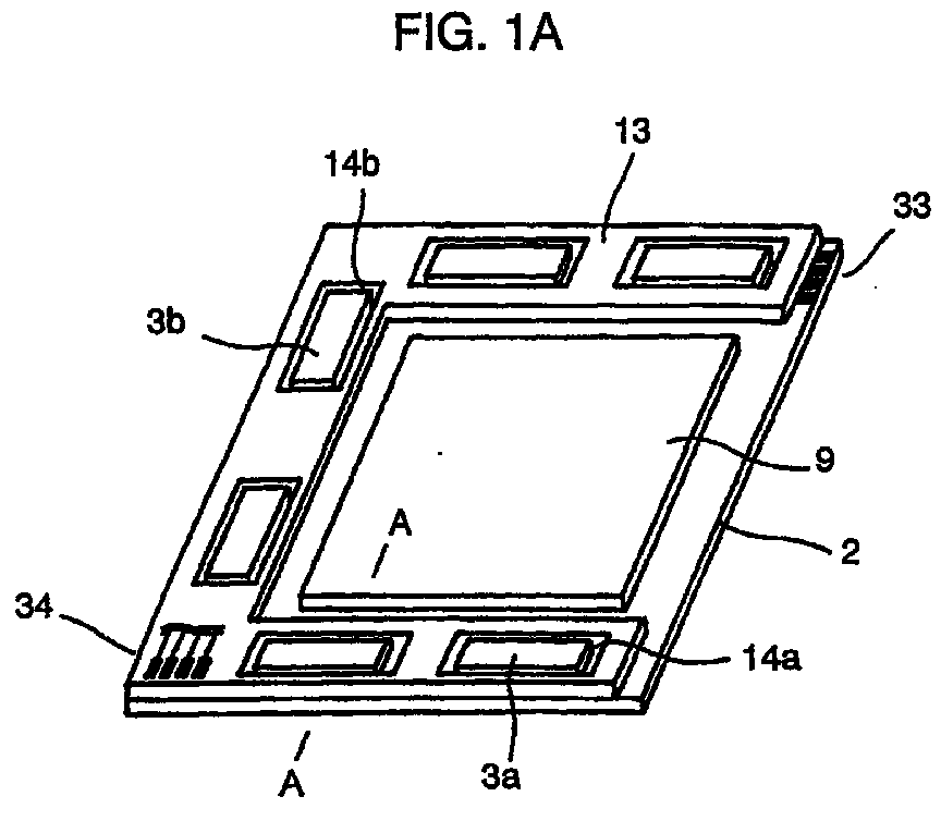
- an active substrate 2 comprises a terminal electrode 5a, a wiring line 7a for connecting this terminal electrode 5a with a signal line, and a wiring line 7b for connecting terminal electrodes 5b, 5c.
- these terminal electrodes 5a, 5b, 5c, and wiring lines 7a, 7b should be formed simultaneously.
- An insulation layer 26 includes gate insulation layer, passivation insulation layer, and other insulation layers formed on a principal surface of the active substrate 2, and insulation layers on the upper surface of the terminal electrodes 5a, 5b, 5c are selectively removed, and the surface of the individual electrodes is exposed.
- a bump electrode 24 connected electrically to the terminal electrodes 5a, 5b is formed.
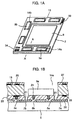
- openings 14a, 14b larger than the outside shape of the integrated circuit chip 3a are formed at positions corresponding to the mounting position of the driving integrated circuit chip 3a mounted on the active substrate 2.
- a wiring line 23 of low resistance is formed, and an insulation layer 27 is formed thereon for the purpose of protecting this wiring line 23.
- the wiring line 23 is formed of a thick conductive material so that its resistance may be low.
- the insulation layer 27 may be formed either at the time of composing the printed circuit board 13, or after mounting the printed circuit board 13 by applying a proper resin. Although not shown, an insulation layer may be similarly formed for protecting a wiring line 22 formed at the mounting surface side of the printed circuit board 13.
- a bump 25 is formed for connecting electrically between the terminal electrode 5c and wiring line 22.
- the wiring line 22 is a wiring line of low resistance formed on the principal surface facing the active substrate 2
- the wiring line 23 is a wiring line of low resistance formed on a principal surface opposite to the principal surface facing the active substrate 2.
- the wiring line of low resistance is generally a copper foil with a film thickness of several to tens of microns.
- the printed circuit board 13 thus composed is mounted on the active substrate 2, first by mounting driving integrated circuit chips 3a, 3b on the active substrate 2 by means of a thermosetting Anisotropic Conductive Film (ACF) or the like.
- ACF Anisotropic Conductive Film
- the printed circuit board 13 forming openings 14a, 14b at positions corresponding to the mounting positions of the mounted driving integrated circuit chips 3a, 3b is mounted outside of the image area of the active substrate 2.
- electric signals are supplied into the terminal electrodes 5a, 5b, 5c of scanning lines and signal lines by mounting the driving integrated circuit chips 3a, 3b directly on the terminal electrodes 5a, 5b disposed on the active substrate 2.
- the electric connection of the driving integrated circuit chips 3a, 3b is made by mounting the printed circuit board 13 on the active substrate 2 so that the openings 14a, 14b of thus composed printed circuit board 13 may be at positions corresponding to the mounting position of the driving integrated circuit chips 3a, 3b mounted on the active substrate 2.
- the mounting method of the printed circuit board 13 on the active substrate 2 is not particularly limited, and, for example, it is fixed by heating while pressing by using the ACF 21.
- the wiring lines 23 of low resistance composed of thick conductive material formed on the printed circuit board 13 can be used as the bus lines such as power source lines, input signal lines or clock lines, it is not necessary to use the conventional long bus flexible film. Besides, since the resistance of the wiring lines 23 is low, signals can be transmitted at high speed without deforming the signal waveform.
- External electric signals can be supplied, as shown in Fig. 1A, by disposing an external connection terminal 33 at a position not interfering mounting of the printed circuit board 13 at the peripheral edge of the active substrate 2 in the same way as in the prior art, or by mounting and connecting by using a Flexible Printed Circuit (FPC) by disposing an external connection terminal 34 on the principal surface opposite to the principal surface of the printed circuit board 13 facing the active substrate 2.
- FPC Flexible Printed Circuit
- the foregoing embodiment 1 employs the printed circuit board 13 forming openings 14a, 14b at positions corresponding to the mounting positions of the driving integrated circuit chips 3a, 3b.
- it is intended to use a printed circuit board 13 having a deep recess 15 larger than the outside shape of the driving integrated circuit chips 3a, 3b, while covering the upper surface of the driving integrated circuit chips 3a, 3b mounted on the active substrate 2.
- This embodiment has the same effects as embodiment 1.
- Fig. 3 explains embodiment 3 of the invention.
- Fig. 3A is a perspective view of the liquid crystal panel
- Fig. 3B is its essential magnified view
- Fig. 3C shows a connection film for linking the split printed circuit boards together.
- the foregoing embodiments 1 and 2 present the L-shaped or pi-shaped printed circuit board 13 integrating a printed circuit board connected to connection terminals of scanning lines and a printed circuit board connected to connection terminals of signal lines. Even when using such printed circuit board 13, in a small-sized liquid crystal panel of size 3 (diagonal 7.5 cm) or smaller, the expansion difference between the printed circuit board 13 and active substrate 2 is small due to temperature rise when mounting the printed circuit board 13, and the material cost and processing cost of the printed circuit board 13 are small, and there is little problem.
- the number of terminals increases and the length is extended at both the disposing side of connection terminals of scanning lines (called scanning line side) and the disposing side of connection terminals of signal lines (called signal line side). Therefore, the length of the printed circuit board 13 is extended, which makes it difficult to use the one-piece type printed circuit board 13.
- the printed circuit board 13 forming a recess 15 at a position corresponding to the mounting position of the driving integrated circuit chip 3 in the same manner as in embodiment 2 is split into the scanning line side and the signal line side as shown in Fig. 3A.
- connection terminals 16a, 16b are formed on the upper surfaces of the both printed circuit boards, and these two groups of connection terminals are connected, as shown in Fig. 3C, by using a flexible connection film 18 connected by a conductive wiring line 10b, for example, between connection terminals 17a and 17b.
- connection method of the connection film 18 to the printed circuit boards 13a, 13b is not specified.
- handling is easy if using a very slender printed circuit board 13 is used. Since handling is easy if the number of parts is increased, and the number of mounting steps and mounting cost are increased by dividing the printed circuit board, sufficient effects for compensating for such demerits are obtained. Accordingly, not only mounting of printed circuit board on the active substrate 2 is easier, but also the total cost is lowered.
- Fig. 4 shows embodiment 4 of the invention.
- Fig. 4A is a perspective view of liquid crystal panel
- Fig. 4B is a magnified view of essential parts thereof.
- connection method of the printed circuit board 13 divided into the scanning line side and signal line side is different from that in embodiment 3, but other basic constitution is nearly in the same manner as in embodiment 3.
- the printed circuit board 13 forming a recess 15 at a position corresponding to the mounting position of the driving integrated circuit chip 3 is split into the scanning line side and signal line side in the same way as in embodiment 2.
- connection film 18 is not used.
- bus lines 10c of power source lines, input signal lines and clock lines are disposed together with connection terminals 19a, 19b, and on the principal surface facing the active substrate 2 of the printed circuit boards 13a, 13b, bus lines 22a, 22b of power source lines, input signal lines and clock lines are disposed together with connection terminals 20a, 20b, and the printed circuit boards 13a, 13b are mounted on the active substrate 2 and connected together.
- Such a constitution can solve the problems of degradation of mounting precision, unevenness of connecting resistance and deterioration of reliability due to the dimensional precision of the printed circuit board 13 or the difference in thermal expansion coefficients between the glass substrate 2 and printed circuit board 13, which occurred conventionally in a large screen sized liquid crystal panel of which one side is more than 10 cm.
- the overall thickness is increased by the portion of the thickness of the flexible connection film 18, but in embodiment 4, since connection film 18 is not used, an increase of overall thickness can be suppressed.
- Fig. 5 explains embodiment 5 of the invention.
- the printed circuit board 13 is divided into a plurality of pieces each at the scanning line side and signal line side, which is different from embodiment 3 and embodiments 4, but other basic constitution is nearly in the same manner as in embodiment 2.
- the printed circuit board each at the scanning line side and signal line side is divided into a plurality of pieces (that is, the scanning line side is divided into 13a, 13b, ..., and the signal line side into 13A, 13B, ).
- bus lines 10c as described above such as power source lines, input signal lines and clock lines are disposed together with connection terminals 19a, 19b between the integrated circuit chips 3a and 3b adjacent to each other in the mounting region outside of the image display area of the active substrate 2.
- Bus lines 22a, 22b such as power source lines, input signal lines and clock lines are disposed together with connection terminals 20a, 20b on the principal surface of the printed circuit boards 13a, 13b facing the active substrate 2.
- the printed circuit boards 13a, 13b are mounted on the active substrate 2 and are connected together.
- bus lines and connection terminals for connecting the split printed circuit boards on a principal surface of the active substrate, it is easy to mount the printed circuit board on the active substrate, in particular, in the display panel of large screen size.
- a connection terminal 34 may be formed on a principal surface at the opposite side of the surface of the printed circuit board 13 facing the active substrate 2. In this case, it is not necessary to change the size if the printed circuit board is divided into a plurality of pieces, but an external connection terminal 34 for connecting with an external circuit needs to be formed in any one of the printed circuit boards.
- embodiment 5 brings about the following effects.
- the material loss is less when fabricating the printed circuit board, so that the cost is saved.
- the expansion difference between the printed circuit board and the active substrate due to heating when mounting the printed circuit board is absorbed, so that the mounting process is easy. Further, the precision of the mounting process is enhanced.
- terminal electrodes for mounting are disposed on a principal surface in the peripheral margin of one glass substrate, and electric signals are supplied from the driving integrated circuit to scanning lines and signal lines by some connecting means, and in this respect they are the same as the liquid crystal panel of the invention.
- the same effects as in embodiments 1 to 5 can be obtained. It is because, in these display devices, too, terminal electrodes for mounting are disposed on a principal surface in the peripheral margin of one glass substrate, and electric signals are supplied from the driving integrated circuit to scanning lines and signal lines by some connecting means.
- a printed circuit board having a deeper recess than the thickness of a driving semiconductor chip, or a printed circuit board having a larger opening than the outside diameter of the driving semiconductor chip is mounted over the driving semiconductor chip mounted on an active substrate.
- wiring lines of low resistance formed on the printed circuit board can be used as bus lines, and the printed circuit board forming wiring lines required to have a low wiring resistance such as power source lines, input signal lines and clock lines can be mounted on the active substrate over each driving integrated circuit chip. Therefore, the mounting cost can be lowered, and the connection around the liquid crystal panel is simplified, so that the reliability of the apparatus can be further enhanced.
- the invention is not limited to the active type color liquid crystal panel alone, and, it is applicable, for example, in the IPS type liquid crystal panel not requiring transparent conductive pixel electrodes, or in the simple type liquid crystal panel not incorporating any active elements, and in the reflection type liquid crystal panel whether of active type or of simple type.
- the invention is also effective in the color liquid crystal panel forming the coloring layers for color display on the active substrate, not on the counter substrate.
Landscapes
- Physics & Mathematics (AREA)
- Nonlinear Science (AREA)
- Mathematical Physics (AREA)
- Chemical & Material Sciences (AREA)
- Crystallography & Structural Chemistry (AREA)
- General Physics & Mathematics (AREA)
- Optics & Photonics (AREA)
- Engineering & Computer Science (AREA)
- Microelectronics & Electronic Packaging (AREA)
- Devices For Indicating Variable Information By Combining Individual Elements (AREA)
- Liquid Crystal (AREA)
Abstract
Description
- 1
- liquid crystal panel
- 2
- active substrate
- 3
- semiconductor integrated circuit chip
- 3a
- semiconductor integrated circuit chip
- 3b
- semiconductor integrated circuit chip
- 4
- TCP film
- 5a
- terminal electrode
- 5b
- terminal electrode
- 6
- terminal electrode
- 7a
- wiring line
- 7b
- wiring line
- 8
- wiring line
- 9
- color filter substrate
- 10a
- common bus line
- 10b
- common bus line
- 10c
- common bus line
- 11
- bus flexible film
- 12
- wiring line
- 13a
- print circuit board
- 13b
- print circuit board
- 14a
- opening
- 14b
- opening
- 15a
- recess
- 15b
- recess
- 16a
- connection terminal
- 16b
- connection terminal
- 17a
- connection terminal
- 17b
- connection terminal
- 18
- flexible connection film
- 19a
- connection terminal
- 19b
- connection terminal
- 20a
- connection terminal
- 20b
- connection terminal
- 21
- ACF
- 22a
- bus line
- 22b
- bus line
- 23
- wiring line
- 24
- bump electrode
- 25
- bump electrode
- 26
- insulation layer
- 27
- insulation layer
Claims (12)
- A display panel including a liquid crystal panel, said liquid crystal panel comprising:an active substrate havinga plurality of scanning lines,a plurality of signal lines substantially orthogonal to the scanning lines sandwiching at least one insulation layer,at least one switching element and at least one pixel electrode at every intersection of the scanning lines and the signal lines, which are all formed on a principal surface of a first transparent insulating substrate, anda terminal electrode of the scanning lines and the signal lines formed outside of an image display area of the active substrate; anda liquid crystal filled between a second transparent insulating substrate or a color filter substrate forming a color filter layer, which are having a transparent conductive layer on a principal surface and facing said active substrate,
wherein electric signals are supplied to terminal electrodes of the scanning lines and the signal lines by mounting a driving integrated circuit chip directly on the terminal electrode disposed on the active substrate, andan electric connection to the driving integrated circuit chip is achieved by mounting a printed circuit board having a larger opening than the outside shape of the driving integrated circuit chip and forming wiring lines at the mounting position of the driving integrated circuit chip mounted on the active substrate and its vicinity, outside of the image display area of the active matrix substrate. - The display panel of claim 1, wherein said printed circuit board mounted outside of the image display area is formed of a same printed circuit board as the printed circuit board also in a portion corresponding to the opening, and covers an upper surface of the driving integrated circuit chip, anda recess deeper and larger than the outside shape of the driving integrated circuit chip is formed around the driving integrated circuit chip.
- The display panel of claim 1 or 2, whereinthe printed circuit board is disposed as being divided into a portion at which the terminal electrode of the scanning lines of the active substrate is disposed and a portion at which the terminal electrode of the signal lines of the active substrate is disposed, anda connection terminal for mutually connecting the divided printed circuit boards is formed on the upper surface of the printed circuit board.
- The display panel of claim 1 or 2, whereinthe printed circuit board is disposed as being divided into a portion at which the terminal electrode of the scanning lines of the active substrate is disposed and a portion at which the terminal electrode of the signal lines of the active substrate is disposed, andwiring lines and connection terminals for mutually connecting the divided printed circuit boards are formed at a mounting surface side of the active substrate.
- The display panel of claim 1 or 2, whereinthe printed circuit board is disposed as being divided into a plurality of pieces each disposed at a portion at which the terminal electrode of the scanning lines of the active substrate is disposed and a portion at which the terminal electrode of the signal lines of the active substrate is disposed, andwiring lines and connection terminals for mutually connecting the divided printed circuit boards are formed on a principal surface of the active substrate.
- A display panel comprising;a plurality of scanning lines;a plurality of signal lines substantially orthogonal to the scanning lines;a terminal electrode of the scanning lines formed outside of an image display area; anda terminal electrode of the signal lines formed outside of the image display area,
wherein electric signals are supplied to the terminal electrode of the scanning lines and the signal lines by mounting a driving integrated circuit chip directly on the terminal electrode, andelectric connection to the driving integrated circuit chip is achieved by mounting a printed circuit board having a larger opening than the outside shape of the driving integrated circuit chip and forming wiring lines at a mounting position of the driving integrated circuit chip and its vicinity; outside of the image display area. - The display panel of claim 6, wherein said printed circuit board mounted outside of the image display area is formed of a same printed circuit board as the printed circuit board also in a portion corresponding to the opening, and covers an upper surface of the driving integrated circuit chip, anda recess deeper and larger than the outside shape of the driving integrated circuit chip is formed around the driving integrated circuit chip.
- The display panel of claim 6 or 7, whereinthe printed circuit board is disposed as being divided into a portion at which the terminal electrode of the scanning lines of the display panel is disposed and a portion at which the terminal electrode of the signal lines of the display panel is disposed, anda connection terminal for mutually connecting the divided printed circuit boards is formed on the upper surface of the printed circuit board.
- The display panel of claim 6 or 7, whereinthe printed circuit board is disposed as being divided into a portion at which the terminal electrode of the scanning lines of the display panel is disposed and a portion at which the terminal electrode of the signal lines of the display panel is disposed, andwiring lines and connection terminals for mutually connecting the divided printed circuit boards are formed at a mounting surface side of one of the substrates for forming the display panel.
- The display panel of claim 6 or 7, whereinthe printed circuit board is disposed as being divided into a plurality of pieces each disposed at a portion at which the terminal electrode of the scanning lines of the display panel is disposed and a portion at which the terminal electrode of the signal lines of the display panel is disposed, andwiring lines and connection terminals for mutually connecting the divided printed circuit boards are formed on a principal surface of one of the substrates for forming the display panel.
- The display panel of any one of claims 6 to 10, wherein said, display panel is any one ofan in-plain-switching (IPS) type liquid crystal panel not requiring transparent conductive pixel electrode,a simple matrix type liquid crystal panel not incorporating active element,a reflection type liquid crystal panel including active matrix type and simple matrix type, anda liquid crystal panel forming coloring layers for color display on an active matrix substrate.
- The display panel of any one of claims 6 to 10, wherein said display panel is an illuminated matrix panel including PDP and EL type.
Applications Claiming Priority (3)
| Application Number | Priority Date | Filing Date | Title |
|---|---|---|---|
| JP11047276A JP3025257B1 (en) | 1999-02-25 | 1999-02-25 | Display panel |
| JP4727699 | 1999-02-25 | ||
| PCT/JP2000/000961 WO2000051099A1 (en) | 1999-02-25 | 2000-02-21 | Display panel |
Publications (2)
| Publication Number | Publication Date |
|---|---|
| EP1079357A1 true EP1079357A1 (en) | 2001-02-28 |
| EP1079357A4 EP1079357A4 (en) | 2007-07-04 |
Family
ID=12770777
Family Applications (1)
| Application Number | Title | Priority Date | Filing Date |
|---|---|---|---|
| EP00904058A Withdrawn EP1079357A4 (en) | 1999-02-25 | 2000-02-21 | Display panel |
Country Status (7)
| Country | Link |
|---|---|
| US (1) | US6424400B1 (en) |
| EP (1) | EP1079357A4 (en) |
| JP (1) | JP3025257B1 (en) |
| KR (1) | KR100397004B1 (en) |
| CN (1) | CN1156734C (en) |
| TW (1) | TW444268B (en) |
| WO (1) | WO2000051099A1 (en) |
Cited By (3)
| Publication number | Priority date | Publication date | Assignee | Title |
|---|---|---|---|---|
| WO2003107085A1 (en) * | 2002-06-13 | 2003-12-24 | ナノックス株式会社 | Liquid crystal display |
| CN100414403C (en) * | 2004-02-25 | 2008-08-27 | 株式会社日立显示器 | display device |
| EP3043203A3 (en) * | 2015-01-08 | 2016-08-03 | Samsung Display Co., Ltd. | Display device with drving circuit |
Families Citing this family (33)
| Publication number | Priority date | Publication date | Assignee | Title |
|---|---|---|---|---|
| JP4381498B2 (en) * | 1999-02-16 | 2009-12-09 | エーユー オプトロニクス コーポレイション | Liquid crystal display device with COG structure |
| JP2001296542A (en) * | 2000-04-11 | 2001-10-26 | Citizen Watch Co Ltd | Liquid crystal display device |
| KR100385082B1 (en) * | 2000-07-27 | 2003-05-22 | 삼성전자주식회사 | a liquid crystal display and a manufacturing method thereof |
| KR100840235B1 (en) * | 2001-08-29 | 2008-06-20 | 삼성전자주식회사 | Liquid crystal display |
| JP2003133677A (en) * | 2001-10-29 | 2003-05-09 | Advanced Display Inc | Pressure-contacting structure of flexible circuit board |
| US7508479B2 (en) * | 2001-11-15 | 2009-03-24 | Samsung Electronics Co., Ltd. | Liquid crystal display |
| US6570339B1 (en) * | 2001-12-19 | 2003-05-27 | Chad Byron Moore | Color fiber-based plasma display |
| KR100846459B1 (en) | 2001-12-26 | 2008-07-16 | 삼성전자주식회사 | Liquid crystal display module having integrated connector and liquid crystal display device having same |
| JP3603890B2 (en) * | 2002-03-06 | 2004-12-22 | セイコーエプソン株式会社 | Electronic device, method of manufacturing the same, and electronic apparatus |
| US7183582B2 (en) * | 2002-05-29 | 2007-02-27 | Seiko Epson Coporation | Electro-optical device and method of manufacturing the same, element driving device and method of manufacturing the same, element substrate, and electronic apparatus |
| JP4059750B2 (en) * | 2002-10-28 | 2008-03-12 | シャープ株式会社 | Electronic module and manufacturing method thereof |
| TWI252954B (en) * | 2002-11-11 | 2006-04-11 | Au Optronics Corp | Liquid crystal display device integrating driving circuit on matrix substrate |
| KR100895311B1 (en) * | 2002-11-19 | 2009-05-07 | 삼성전자주식회사 | Liquid Crystal Display and Inspection Method |
| JP3895697B2 (en) * | 2003-03-03 | 2007-03-22 | 日東電工株式会社 | Flexible printed circuit board |
| KR100637429B1 (en) * | 2003-10-24 | 2006-10-20 | 삼성에스디아이 주식회사 | Plasma display device |
| US7139060B2 (en) * | 2004-01-27 | 2006-11-21 | Au Optronics Corporation | Method for mounting a driver IC chip and a FPC board/TCP/COF device using a single anisotropic conductive film |
| JP4521205B2 (en) * | 2004-02-27 | 2010-08-11 | オプトレックス株式会社 | LCD panel |
| JP4490719B2 (en) * | 2004-04-02 | 2010-06-30 | 東芝モバイルディスプレイ株式会社 | Liquid crystal display |
| US7315116B2 (en) * | 2004-07-09 | 2008-01-01 | Au Optronics Corporation | Organic electroluminescent display device with separately connected signal lines and power lines |
| JP3979405B2 (en) * | 2004-07-13 | 2007-09-19 | セイコーエプソン株式会社 | Electro-optical device, mounting structure, and electronic apparatus |
| CN100353309C (en) * | 2004-11-01 | 2007-12-05 | 南京Lg同创彩色显示系统有限责任公司 | Input signal distinguishing apparatus of image display device |
| KR20060039658A (en) * | 2004-11-03 | 2006-05-09 | 엘지전자 주식회사 | Organic electroluminescent device kit |
| KR100649566B1 (en) * | 2005-07-07 | 2006-11-27 | 삼성에스디아이 주식회사 | Plasma display panel |
| KR100637233B1 (en) * | 2005-08-19 | 2006-10-20 | 삼성에스디아이 주식회사 | Plasma display panel |
| JP2007080969A (en) * | 2005-09-12 | 2007-03-29 | Sony Corp | Printed wiring board and its manufacturing method |
| JP2008020836A (en) * | 2006-07-14 | 2008-01-31 | Nec Lcd Technologies Ltd | Display device and manufacturing method thereof |
| KR101340296B1 (en) * | 2007-02-02 | 2013-12-11 | 삼성디스플레이 주식회사 | Flexible printed circuit and display device having the same |
| JP5199699B2 (en) * | 2008-02-29 | 2013-05-15 | シチズンファインテックミヨタ株式会社 | Transmission type liquid crystal display device and manufacturing method thereof |
| JP4713659B2 (en) * | 2009-09-15 | 2011-06-29 | シャープ株式会社 | Liquid crystal display device |
| KR101989824B1 (en) * | 2012-12-07 | 2019-06-17 | 삼성전자주식회사 | Display module |
| TWI527505B (en) * | 2013-01-10 | 2016-03-21 | 元太科技工業股份有限公司 | A circuit substrate structure and a method for manufacturing thereof |
| US9589521B2 (en) * | 2014-11-20 | 2017-03-07 | Shenzhen China Star Optoelectronics Technology Co., Ltd. | Liquid crystal display apparatus having wire-on-array structure |
| US12601947B2 (en) | 2022-05-18 | 2026-04-14 | Beijing Boe Display Technology Co., Ltd. | Display module, display device and driving circuit board |
Family Cites Families (13)
| Publication number | Priority date | Publication date | Assignee | Title |
|---|---|---|---|---|
| JP3038747B2 (en) | 1989-12-26 | 2000-05-08 | 株式会社デンソー | Liquid crystal display element alignment treatment method |
| JPH04181985A (en) * | 1990-11-16 | 1992-06-29 | Sanyo Electric Co Ltd | Liquid crystal display device |
| JPH05181985A (en) | 1991-12-27 | 1993-07-23 | Rohm Co Ltd | Non-fuzzy device |
| JP3196181B2 (en) | 1992-04-28 | 2001-08-06 | 日本曹達株式会社 | Reaction endpoint control method using ORP electrode |
| JPH06148671A (en) * | 1992-11-13 | 1994-05-27 | Sharp Corp | Panel mounting structure |
| US5592365A (en) * | 1993-12-21 | 1997-01-07 | Sharp Kabushiki Kaisha | Panel assembly structure and panel assembling method capable of achieving a highly reliable connection of electrode terminals even when the electrode terminals have a fine pitch |
| US6144216A (en) * | 1995-04-01 | 2000-11-07 | Enplas Corporation | Electric contact apparatus for inspecting a liquid crystal display panel |
| GB2307598B (en) * | 1995-11-24 | 2000-02-23 | Varintelligent | Combined printed circuit board and integrated circuit driver |
| US6089442A (en) * | 1996-04-10 | 2000-07-18 | Canon Kabushiki Kaisha | Electrode connection method |
| JPH1068964A (en) * | 1996-08-29 | 1998-03-10 | Kyocera Corp | Liquid crystal display |
| JPH1096948A (en) | 1996-09-19 | 1998-04-14 | Matsushita Electric Ind Co Ltd | Liquid crystal display |
| JPH10274779A (en) | 1997-03-31 | 1998-10-13 | Matsushita Electric Ind Co Ltd | Liquid crystal display panel and method of manufacturing the same |
| KR100268665B1 (en) * | 1997-06-27 | 2000-10-16 | 윤종용 | Method and device for mounting lcd to printed circuit board in a portable communication terminal |
-
1999
- 1999-02-25 JP JP11047276A patent/JP3025257B1/en not_active Expired - Fee Related
-
2000
- 2000-02-21 WO PCT/JP2000/000961 patent/WO2000051099A1/en not_active Ceased
- 2000-02-21 CN CNB00800224XA patent/CN1156734C/en not_active Expired - Fee Related
- 2000-02-21 KR KR10-2000-7011537A patent/KR100397004B1/en not_active Expired - Fee Related
- 2000-02-21 EP EP00904058A patent/EP1079357A4/en not_active Withdrawn
- 2000-02-21 US US09/673,357 patent/US6424400B1/en not_active Expired - Fee Related
- 2000-02-23 TW TW089103167A patent/TW444268B/en not_active IP Right Cessation
Cited By (4)
| Publication number | Priority date | Publication date | Assignee | Title |
|---|---|---|---|---|
| WO2003107085A1 (en) * | 2002-06-13 | 2003-12-24 | ナノックス株式会社 | Liquid crystal display |
| CN100414403C (en) * | 2004-02-25 | 2008-08-27 | 株式会社日立显示器 | display device |
| EP3043203A3 (en) * | 2015-01-08 | 2016-08-03 | Samsung Display Co., Ltd. | Display device with drving circuit |
| US10152943B2 (en) | 2015-01-08 | 2018-12-11 | Samsung Display Co., Ltd. | Display device |
Also Published As
| Publication number | Publication date |
|---|---|
| KR100397004B1 (en) | 2003-09-03 |
| CN1294730A (en) | 2001-05-09 |
| CN1156734C (en) | 2004-07-07 |
| WO2000051099A1 (en) | 2000-08-31 |
| JP2000250427A (en) | 2000-09-14 |
| KR20010042794A (en) | 2001-05-25 |
| JP3025257B1 (en) | 2000-03-27 |
| EP1079357A4 (en) | 2007-07-04 |
| TW444268B (en) | 2001-07-01 |
| US6424400B1 (en) | 2002-07-23 |
Similar Documents
| Publication | Publication Date | Title |
|---|---|---|
| US6424400B1 (en) | Display panel including a printed circuit board having a larger opening than the outside shape of the driving IC chip | |
| KR100391843B1 (en) | packaging method of liquid crystal displays and the structure thereof | |
| RU2458491C1 (en) | Flexible substrate and structure of electric circuit | |
| US6734941B2 (en) | Liquid crystal display device | |
| KR100769160B1 (en) | Test pad for testing liquid crystal display device | |
| KR100321883B1 (en) | Structure and method of mounting semiconductor device and liquid crystal display device | |
| US7876122B2 (en) | Display device | |
| EP1391774B1 (en) | Liquid crystal display | |
| US7019808B2 (en) | Image device | |
| KR20090058987A (en) | Manufacturing method of liquid crystal display device and manufacturing method of film carrier tape of liquid crystal display device | |
| KR100496087B1 (en) | Electro-optical device and electronic device | |
| US20020118332A1 (en) | Liquid crystal display device | |
| KR100943731B1 (en) | Seaoji display device | |
| KR20040087452A (en) | Liquid crystal display module | |
| KR101394920B1 (en) | Chip on glass type liquid crystal display device | |
| JP4343328B2 (en) | Display device | |
| JP3613151B2 (en) | Display device | |
| JP2001264794A (en) | Method for manufacturing liquid crystal display device | |
| JPH08292443A (en) | Liquid crystal display device and manufacturing method thereof | |
| JP3286587B2 (en) | Liquid crystal panel and luminescent matrix panel | |
| EP3786698B1 (en) | Auxiliary coupling layer and display device having the same | |
| JP2004361443A (en) | Display device and method for manufacturing the display device | |
| JPH11183924A (en) | Liquid crystal display device | |
| KR20060125326A (en) | Liquid crystal display | |
| KR20070106261A (en) | LCD Display |
Legal Events
| Date | Code | Title | Description |
|---|---|---|---|
| PUAI | Public reference made under article 153(3) epc to a published international application that has entered the european phase |
Free format text: ORIGINAL CODE: 0009012 |
|
| 17P | Request for examination filed |
Effective date: 20001025 |
|
| AK | Designated contracting states |
Kind code of ref document: A1 Designated state(s): AT BE CH CY DE DK ES FI FR GB GR IE IT LI LU MC NL PT SE |
|
| RBV | Designated contracting states (corrected) |
Designated state(s): DE FR GB |
|
| RAP1 | Party data changed (applicant data changed or rights of an application transferred) |
Owner name: TOSHIBA MATSUSHITA DISPLAY TECHNOLOGY CO., LTD. |
|
| A4 | Supplementary search report drawn up and despatched |
Effective date: 20070601 |
|
| RIC1 | Information provided on ipc code assigned before grant |
Ipc: H05K 1/18 20060101ALN20070525BHEP Ipc: G09F 9/00 20060101ALI20070525BHEP Ipc: H05K 1/14 20060101ALN20070525BHEP Ipc: G02F 1/13 20060101AFI20070525BHEP |
|
| STAA | Information on the status of an ep patent application or granted ep patent |
Free format text: STATUS: THE APPLICATION HAS BEEN WITHDRAWN |
|
| 18W | Application withdrawn |
Effective date: 20070710 |