EP1069683B1 - Circuit de commande pour un commutateur semi-conducteur de puissance - Google Patents
Circuit de commande pour un commutateur semi-conducteur de puissance Download PDFInfo
- Publication number
- EP1069683B1 EP1069683B1 EP00306006A EP00306006A EP1069683B1 EP 1069683 B1 EP1069683 B1 EP 1069683B1 EP 00306006 A EP00306006 A EP 00306006A EP 00306006 A EP00306006 A EP 00306006A EP 1069683 B1 EP1069683 B1 EP 1069683B1
- Authority
- EP
- European Patent Office
- Prior art keywords
- turn
- power semiconductor
- semiconductor switch
- switching element
- gate
- Prior art date
- Legal status (The legal status is an assumption and is not a legal conclusion. Google has not performed a legal analysis and makes no representation as to the accuracy of the status listed.)
- Expired - Lifetime
Links
- 239000004065 semiconductor Substances 0.000 title claims description 118
- 230000015556 catabolic process Effects 0.000 claims description 9
- 230000006698 induction Effects 0.000 claims description 2
- 230000003068 static effect Effects 0.000 claims description 2
- 239000003990 capacitor Substances 0.000 description 18
- 238000010586 diagram Methods 0.000 description 6
- 230000003247 decreasing effect Effects 0.000 description 5
- 238000000034 method Methods 0.000 description 2
- 238000011084 recovery Methods 0.000 description 2
- 238000007599 discharging Methods 0.000 description 1
- 238000012986 modification Methods 0.000 description 1
- 230000004048 modification Effects 0.000 description 1
Images


Classifications
-
- H—ELECTRICITY
- H03—ELECTRONIC CIRCUITRY
- H03K—PULSE TECHNIQUE
- H03K17/00—Electronic switching or gating, i.e. not by contact-making and –breaking
- H03K17/04—Modifications for accelerating switching
- H03K17/0403—Modifications for accelerating switching in thyristor switches
-
- H—ELECTRICITY
- H02—GENERATION; CONVERSION OR DISTRIBUTION OF ELECTRIC POWER
- H02M—APPARATUS FOR CONVERSION BETWEEN AC AND AC, BETWEEN AC AND DC, OR BETWEEN DC AND DC, AND FOR USE WITH MAINS OR SIMILAR POWER SUPPLY SYSTEMS; CONVERSION OF DC OR AC INPUT POWER INTO SURGE OUTPUT POWER; CONTROL OR REGULATION THEREOF
- H02M1/00—Details of apparatus for conversion
- H02M1/08—Circuits specially adapted for the generation of control voltages for semiconductor devices incorporated in static converters
Definitions
- the present invention relates to a gate driving circuit for a power semiconductor switch, and more particularly to a pulse driving circuit for driving abruptly or steeply a power semiconductor switch into a conductive state at a very high speed.
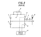
- Fig. 1 is an example of known gate driving circuits for driving a power semiconductor switch in a pulse mode.
- a first DC voltage source 1 for turning-on a semiconductor switch and a second DC voltage source 2 for turning-off a semiconductor switch are provided.
- a series circuit of a resistor 3 and a capacitor 4 is connected across the turn-on DC voltage source 1, and a junction point between the resistor 3 and the capacitor 4 is coupled with a gate G of a power semiconductor switch 6 by means of a turn-on switching element 5.
- a stray inductance contained in a circuit portion from the DC voltage source to the gate G of the power semiconductor switch 6 is represented as an inductor 7 which is connected between the turn-on switching element 5 and the gate G of the power semiconductor switch 6.
- the above mentioned resistor 3 serves not only as a charging resistor for the capacitor 4 but also as a resistor for supplying a current to the gate G of the power semiconductor switch 6 for maintaining the power semiconductor switch in the conducting state.
- a cathode K of the power semiconductor switch 6 is connected to a negative terminal of the turn-on DC voltage source 1, and a junction point between the turn-on switching element 5 and the inductor 7 is coupled with a negative terminal of the turn-off DC voltage source 2 by means of a turn-off switching element 8.
- the turn-on and turn-off switching elements 5 and 8 are controlled by a control circuit 9.
- the turn-on switching element 5 is switched from “off” to “on”, and then energy stored in the capacitor 4 flows through the turn-on switching element 5 to the gate G of the power semiconductor switch 6, and further flows to the cathode K of the semiconductor switch.
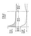
- a maximum value of the current flowing from the gate G to the cathode K of the power semiconductor switch 6 is denoted as I 2 in Fig. 2. Since the large current I 2 flows to the gate G of the power semiconductor switch 6, this switch is turned-on and a large current flows through the anode-cathode A-K path by means of main DC voltage supply source not shown. After that, the power semiconductor switch 6 is kept conductive as long as the current flows into the gate G of the power semiconductor switch.
- the turn-on switching element 5 is turned-off and the turn-off switching element 8 is turned-on by the control circuit 9, and then the power semiconductor switch 6 is turned-off.
- the stray inductance L s is about 100 nH and the raising rate (di G /dt) of the gate current is required not less than 3000 A/ ⁇ s. Therefore, the voltage E 1 of the turn-on DC voltage source 1 has to be not lower than 300 V.
- An amount of charge Q to be supplied to the gate G of the power semiconductor switch 6 for turning-on the power semiconductor switch at a high speed is determined by respective switches.
- This amount of charge Q is identical with an amount of charge stored in the capacitor 4, and its energy is represented by 1/2 ⁇ QE 1 .
- An energy loss in the resistor 3 for storing such energy is also expressed by 1/2 ⁇ QE 1 . Therefore, the turn-on DC voltage source 1 has to supply a sum of these energy and is equal to QE 1 .
- the capacitor 4 has a capacitance of 0.5 ⁇ F and a pulse repetition frequency is 2 KHz. Then the turn-on DC voltage source 1 must supply a power of 90 W. Since the turn-on DC voltage source 1 must supply the current for keeping the power semiconductor switch 6 conductive for 50 ⁇ s, and this current amounts to a power of 30 W. Therefore, the turn-on voltage source 1 must supply a sum of these powers which amounts to a very large value of 120 W.
- JP-A-60-22464 shows a circuit corresponding to the first part of present claim 1.
- the present invention has for its object to provide a novel and useful gate driving circuit for a power semiconductor switch, in which the above mentioned drawbacks of the known gate driving circuits and the semiconductor switch can be driven in the pulse mode by flowing abruptly a large current to a gate of the power semiconductor switch.
- a gate driving circuit for driving a power semiconductor switch in a pulse mode is provided, as set out in claim 1.
- said reactor is utilized as an energy storing means, to which a current flows from the DC voltage source having a lower output voltage such that the current increases to a desired value, and a sharply increasing gate current is flown into the gate of the power semiconductor switch by utilizing a high voltage which is induced upon discharging the energy stored in the reactor. Therefore, it is possible to realize the gate driving circuit for power semiconductor switch having a low loss as well as a high performance.
- each of said first and second switching elements is formed by a semiconductor switching element.
- said first switching element is changed into the off-state to prepare a next turning-on operation.
- said first switching element by a semiconductor switching element and to construct said second switching element by a semiconductor switching element which is made conductive by breakdown by an inversely induced voltage across the reactor when the second switching element is changed from the turn-on state to the turn-off state.
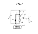
- Fig. 4 is a circuit diagram illustrating an embodiment of the gate driving circuit for a power semiconductor switch according to the invention.
- a positive output terminal of a DC voltage source 11 is connected to a cathode K of a power semiconductor switch 12, and a series circuit of a turn-on switching element 13 and a reactor 14 is connected across the positive output terminal of the DC voltage source 11 and a gate G of the power semiconductor switch 12.
- an inductance 15 which represents a stray inductance.
- a junction point between the reactor 14 and the gate G of the power semiconductor switch 12 is connected to a negative output terminal of the DC voltage source 11 by means of a turn-off switching element 16.
- a freewheel diode 17 is connected across a junction point between the turn-on switching element 13 and the reactor 14 and the negative output terminal of the DC voltage source 11 such that the anode of the freewheel diode 17 is connected to the negative output terminal of the DC voltage source 11. Furthermore, the gate driving circuit comprises a control circuit 18 for controlling on-state and off-state of the turn-on and turn-off switching elements 13 and 16.
- the current flowing through the reactor 14 arrives at a desired value I 1 , and at that time, the turn-off switching element 16 is changed from the on-state to the off-state. Then, the current which has been flowing through the reactor 14 is going to flow into the gate G of the power semiconductor switch 12. However, since the stray inductance is existent between the gate G and the cathode K of the power semiconductor switch 12 as shown by the inductor 15 in Fig. 4, the current flowing through the reactor 14 could not be promptly changed, and therefore a relatively high inversely induced voltage is generated across the reactor 14.
- the turn-off switching element 16 is constructed by a semiconductor switching element which undergoes breakdown at its maximum rated voltage to absorb a part of the energy induced by the reactor 14.
- a semiconductor device may be "HEXFET" sold by International Rectifier Corporation.
- the stray inductance L S denoted by the inductor 15 is 100 nH
- the increasing rate di G /dt of the gate current i G is 3000 A/ ⁇ s and the voltage E of the DC voltage source 11 is 30V
- the breakdown voltage V B of the turn-off semiconductor switching device 16 may be set to 330 V.
- This current is gradually decreased by a loss in the circuit, but a larger amount of charges can be supplied to the gate G of the power semiconductor switch 12 as a continuous-on-current than the known gate driving circuit.
- the energy required for keeping the power semiconductor switch in the conduction state is obtained not from the DC voltage source 11, but from the residual energy remained in the reactor 14. This is a remarkable difference of the present invention from the prior art.
- the turn-on switching element 13 is changed from the on-state into the off-state and the turn-off switching element 16 is changed from the off-state into the on-state by means of the control circuit 18.
- the cathode K of the power semiconductor switch 12 is connected to the positive output terminal of the DC voltage source 11 and the gate G is connected to the negative output terminal. In this manner, the gate-cathode of the power semiconductor switch 12 is reverse-biased and is turned-off positively.
- the turn-on switching element 13 is changed from the off-state into the on-state at the instant t 0 , and is driven from the on-state into the off-state at the instant t 5 .
- the turn-off switching element 16 is changed from the on-state into the off-state at the instant t 1 and is driven from the off-state into the on-state at the instant t 5 . Therefore, after the power semiconductor switch 12 has been made on, the magnetic energy in the reactor 14 circulates through the gate-cathode of the power semiconductor switch and the turn-on switching element 13, and an excessive large current flows into the gate of the power semiconductor switch 12. Such an unnecessarily large gate current introduces a circuit loss and an operating efficiency of the whole gate driving circuit might be decreased.
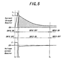
- Fig. 6 is a graph showing an operation of another embodiment of the gate driving circuit for power semiconductor switch according to the invention.
- the structure of the gate driving circuit of the present embodiment is identical with that shown in Fig. 4, but the manner of driving the turn-on switching element 13 by the control circuit 18 differs from that of the previous embodiment. Now the operation will be explained in greater detail than the previous embodiment.
- a mode I the power semiconductor switch 12 is in the off-state, and the turn-on switching element 13 is in the off-state and the turn-off switching element 16 is in the on-state. Since the voltage E of the DC voltage source 11 is applied across the gate G and the cathode K of the power semiconductor switch 12 in a reverse polarity, and therefore the power semiconductor switch is positively kept in the off-state. It should be noted that in this mode I, the current flowing through the reactor 14 is zero.
- a mode II is a preparing period for turning-on the power semiconductor switch 12. During this mode II, the turn-on switching element 13 is made conductive by the control circuit 18 and the voltage E of the DC voltage source 11 is applied to the reactor 14 and the current flowing through the reactor 14 is increased to I 1 .
- the turn-off switching element 16 is driven into the off-state by the control circuit 18 at the instant t 1 .
- the current flowing through the reactor 14 tends to flow into the gate G of the power semiconductor switch 12.
- the current could not flow immediately due to the stray inductance of a circuit portion connected to the gate G of the power semiconductor switch 12, and therefore an excessively large reverse voltage produced across the reactor 14.
- this reverse voltage is also applied to the turn-off switching element 16 and if the reverse voltage exceeds the rated voltage of the turn-off switching element 16, this switching element is broken.
- This problem of the breakdown of the turn-off switching element can be resolved by constructing the turn-off switching element 16 by a power MOSFET which is broken down at a predetermined breakdown voltage, can absorb the surge current and has a low on-resistance.
- a power MOSFET is manufactured and sold by International Rectifier Corporation.
- the turn-off switching element 16 has a breakdown voltage E b
- the reactor 14 is clamped at a voltage of (E b - E).
- This voltage is also applied to the stray inductance 15 surrounding the gate G of the power semiconductor switch 12, and therefore the gate current increases abruptly.
- the gate current becomes identical with the current passing through the reactor 14, the clamped state is released to complete this mode III.
- This time period is a gate current raising period, and therefore if it is required to flow the gate current with the raising inclination di/dt substantially identical with the known gate driving circuit, the voltage (E b - E) has to be set to 300 V. Since the period of the mode III is very short such as 50 ns, the energy used in this mode is not so high, although an instantaneous power is very large. At the end of the mode III, the current flowing through the reactor 14 has been decreased to I 2 .
- a next mode IV is a first circulating period.
- the turn-on switching element 13 In order to make the gate current not to descend abruptly after the clamp period has been completed, the turn-on switching element 13 is kept in the on-state for a very short time after the turn-off switching element 16 is changed into the off-state at the instant t 1 .
- the current circulates from the reactor 14 through the gate G - cathode K of the power semiconductor switch 12-turn-on switching element 13. It should be noted that according to the invention, it is not always necessary to provide such a circulating period.
- the gate current At the end of the first circulating period, the gate current has been reduced to I 3 .
- a next mode V is a specific to the present embodiment. If the above explained first circulating mode IV is continued as it is, an excessive amount of charge is injected into the gate of the power semiconductor switch 12 and the energy stored in the reactor 14 is wasted.
- the gate current is abruptly deceased to a level necessary for keeping continuously the power semiconductor switch 12 in the on-state. To this end, at an instant t 3 , the turn-on switching element 13 is changed into the off-state. Then, the current so far flowing through turn-on switching element 13 is switched to flow through the freewheel diode 17.
- a next mode VI is a second circulating period.
- the turn-on switching element 13 is made on, and therefore the gate current required for keeping the power semiconductor switch 12 in the turn-on state continuously, i.e. the continuous-on-current I 4-5 of about 1 A flows for a necessary time period such as about 50 ⁇ s. It is desired to make a decreasing rate of the gate current as small as possible.
- a last mode VII is a turn-off period.
- the turn-on switching element 13 is changed into the off-state and the turn-off switching element 16 is made on under the control of the control circuit 18 to turn-off the power semiconductor switch 12, and after that the power semiconductor switch is remained in the off-state.
- the voltage E of the DC voltage source 11 is applied across the gate and the cathode of the power semiconductor switch 12 with a reverse polarity. Then, a gate drawing current flows from the cathode to the gate of the power semiconductor switch 12, and therefore the power semiconductor switch is positively turned-off.
- the gate drawing current flows only slightly.
- the turn-on switching element 13 and turn-off switching element 16 are changed into the off-state and on-state, respectively at the same time, but according to the invention, these switching elements may be driven at slightly different timings. That is to say, even if both the switching elements 13 and 16 are in the on-state for a short time period, a large short-circuit current does not flow, because the reactor 14 is connected in series with these switching elements.
- the turn-off switching element 16 is made on, a closed circuit of reactor 14 - switching element 16 - freewheel diode 17 -reactor 14 is established, and an initial current I 5 circulates through this circuit. Then, a residual energy in the reactor 14 is wasted as the circuit loss. Therefore, if a value of the initial current I 5 is determined, it is advantageous to set the inductance of the reactor 14 as small as possible.
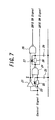
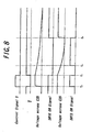
- Fig. 7 is a circuit diagram showing an embodiment of the control circuit 18, and Fig. 8 depicts signal waveforms for explaining the operation of the control circuit.
- the driving signals for the turn-on and turn-off switching elements 13 and 16 are generated on the basis of a control signal S shown in Fig. 8.
- the control signal S is supplied to an inverter 21 to produce an inverted control signal S .
- the control signal S is applied to one input terminal of NAND circuit 24 by means of a parallel circuit of a resistor 22 and a diode 23.
- the inverted control signal S is applied to the other input terminal of the NAND circuit 24.
- the one input terminal of the NAND circuit 24 is connected to a capacitor 25 which determines a discharge time constant together with the resistor 22.
- An output terminal of the NAND circuit 24 is connected to one input terminal of NAND circuit 28 via a parallel circuit of a resistor 26 and a diode 27, and the inverted control signal S is applied to the other input terminal of the NAND circuit 28.
- the one input terminal of the NAND circuit 28 is connected to a capacitor 29 which determines a discharge time constant together with the resistor 26.
- the driving signal for the turn-off switching element 16 is derived from the NAND circuit 24, and the driving signal for the turn-on switching element 13 is produced by the NAND circuit 28.
- the start timings of the succeeding modes IV-VII can be determined by suitably setting time constants of the resistors and capacitors of the control circuit.
- the power semiconductor switch is formed by the gate turn off thyristor (GTO), but it may be constructed any other power semiconductor switches such as IGBT, thyristor, SI thyristor and bipolar transistor.
- GTO gate turn off thyristor
- turn-on and turn-off switching elements are preferably formed by semiconductor switching elements, and particularly they may advantageously constructed by bipolar transistor and MOSFET. Furthermore, the freewheel diode may be replaced by a semiconductor switching element.
- the gate driving circuit for power semiconductor switch it is possible to supply the abruptly increasing gate current with a small power by a simple circuit.
- the current recovery period in which the current flowing through the reactor is changed to flow into the DC voltage source through the freewheel diode by making the turn-on switching element off after the current through the reactor reached its peak value. Therefore, the magnetic energy stored in the reactor can be recovered by the DC voltage source and the power consumption can be further reduced.
Landscapes
- Engineering & Computer Science (AREA)
- Power Engineering (AREA)
- Power Conversion In General (AREA)
Claims (5)
- Circuit conducteur de porte logique pour un interrupteur à semi-conducteur de puissance (12) comprenant :caractérisé en ce que ledit élément de commutation d'arrêt (16) est raccordé à la porte logique (G) de l'interrupteur à semi-conducteur de puissance et à ladite borne de sortie négative de la source de tension à courant continu ; etune source de tension à courant continu (11) dotée de bornes de sortie positive et négative, ladite borne de sortie positive étant raccordée à une cathode (K) de l'interrupteur à semi-conducteur de puissance (12) ;un circuit de courant d'un réacteur (14) et un élément de commutation de marche (13), ledit circuit de courant étant raccordé à la borne de sortie positive de la source de tension à courant continu et à une porte logique (G) de l'interrupteur à semi-conducteur de puissance (12) ;un élément de commutation d'arrêt (16) ;un circuit de commande (18) pour commander lesdits éléments de commutation de marche et d'arrêt (13, 16) de sorte que (i) ledit interrupteur à semi-conducteur de puissance est maintenu dans un état non conducteur en mettant lesdits éléments de commutation de marche et d'arrét à l'état d'arrêt et de marche respectivement, (ii) pour activer l'interrupteur à semi-conducteur de puissance, après avoir stocké l'énergie dans ledit réacteur (14) en faisant passer ledit élément de commutation de marche (13) de l'état désactivé à l'état activé, l'énergie stockée dans le réacteur (14) est évacuée brusquement dans la porte logique (G) de l'interrupteur à semi-conducteur de puissance en faisant passer ledit élément de commutation d'arrêt (16) de l'état activé à l'état désactivé ;
il existe une diode libre (17) dont l'anode est raccordée à la borne de sortie négative de la source de tension à courant continu et dont la cathode est raccordée à un point de jonction entre l'élément de commutation de marche (13) et le réacteur (14). - Circuit conducteur de porte logique pour un interrupteur à semi-conducteur de puissance selon la revendication 1, dans lequel chacun desdits éléments de commutation de marche et d'arrêt (13, 16) est formé par un élément de commutation à semi-conducteur.
- Circuit conducteur de porte logique pour un interrupteur à semi-conducteur de puissance selon la revendication 2, dans lequel ledit circuit de commande est construit de sorte qu'après avoir activé ledit interrupteur à semi-conducteur de puissance, ledit élément de commutation de marche (13) est maintenu à l'état désactivé pour faire passer un courant de porte logique à la porte logique de l'interrupteur à semi-conducteur de puissance et en même temps, l'énergie stockée dans ledit réacteur (14) retourne dans la source de tension à courant continu par le biais de la diode libre, alors que le courant de la porte logique passe dans la porte logique de l'interrupteur à semi-conducteur de puissance, et ensuite ledit élément de commutation de marche (13) passe à nouveau à l'état activé de sorte que le courant de porte logique nécessaire pour maintenir l'interrupteur à semi-conducteur de puissance conducteur, est produit par l'énergie encore stockée dans le réacteur (14).
- Circuit conducteur de porte logique pour un interrupteur à semi-conducteur de puissance selon la revendication 3, dans lequel ledit élément de commutation d'arrêt (16) est formé par un élément de commutation à semi-conducteur qui est rendu conducteur par la rupture due à une tension induite inversement sur ledit réacteur (14) lorsque ledit élément de commutation d'arrêt (16) passe de l'état activé à l'état désactivé.
- Circuit conducteur de porte logique pour un interrupteur à semi-conducteur de puissance selon l'une quelconque des revendications 1-4, dans lequel ledit interrupteur à semi-conducteur de puissance (12) est formé par un interrupteur choisi parmi un thyristor interrupteur, un transistor bipolaire à porte isolée, un thyristor, un thyristor à induction statique et un transistor bipolaire.
Applications Claiming Priority (4)
| Application Number | Priority Date | Filing Date | Title |
|---|---|---|---|
| JP20116399 | 1999-07-15 | ||
| JP20116399 | 1999-07-15 | ||
| JP2000058216 | 2000-03-03 | ||
| JP2000058216A JP4080129B2 (ja) | 1999-07-15 | 2000-03-03 | 電力用半導体スイッチのゲート駆動回路 |
Publications (3)
| Publication Number | Publication Date |
|---|---|
| EP1069683A2 EP1069683A2 (fr) | 2001-01-17 |
| EP1069683A3 EP1069683A3 (fr) | 2001-05-02 |
| EP1069683B1 true EP1069683B1 (fr) | 2003-10-08 |
Family
ID=26512612
Family Applications (1)
| Application Number | Title | Priority Date | Filing Date |
|---|---|---|---|
| EP00306006A Expired - Lifetime EP1069683B1 (fr) | 1999-07-15 | 2000-07-14 | Circuit de commande pour un commutateur semi-conducteur de puissance |
Country Status (5)
| Country | Link |
|---|---|
| US (1) | US6268754B1 (fr) |
| EP (1) | EP1069683B1 (fr) |
| JP (1) | JP4080129B2 (fr) |
| KR (1) | KR100385789B1 (fr) |
| DE (1) | DE60005758T2 (fr) |
Families Citing this family (8)
| Publication number | Priority date | Publication date | Assignee | Title |
|---|---|---|---|---|
| JP4565773B2 (ja) * | 2001-05-31 | 2010-10-20 | 日本碍子株式会社 | 高電圧パルス発生回路 |
| JP4622856B2 (ja) * | 2003-06-05 | 2011-02-02 | トヨタ自動車株式会社 | モータ駆動装置、それを搭載した自動車および電圧変換の制御をコンピュータに実行させるためのプログラムを記録したコンピュータ読取り可能な記録媒体 |
| US7458504B2 (en) * | 2006-10-12 | 2008-12-02 | Huhtamaki Consumer Packaging, Inc. | Multi walled container and method |
| JP5258706B2 (ja) * | 2009-08-25 | 2013-08-07 | 東芝三菱電機産業システム株式会社 | 半導体電力変換装置のゲート駆動回路 |
| US8830647B2 (en) | 2012-05-24 | 2014-09-09 | Mersen Usa Newburyport-Ma, Llc | Fault current limiter |
| EP2793397B1 (fr) * | 2013-04-19 | 2016-01-13 | ABB Technology AG | Dispositif de commutation de courant avec IGCT |
| RU2605454C1 (ru) * | 2015-08-19 | 2016-12-20 | Акционерное общество "ТВЭЛ" (АО "ТВЭЛ") | Адаптивное устройство для управления силовым тиристором |
| KR102327683B1 (ko) * | 2019-12-26 | 2021-11-17 | 엘지전자 주식회사 | 전력 변환 장치 |
Family Cites Families (13)
| Publication number | Priority date | Publication date | Assignee | Title |
|---|---|---|---|---|
| US4136382A (en) * | 1978-01-18 | 1979-01-23 | Exxon Research & Engineering Co. | Converter system |
| JPS5545276A (en) | 1978-09-27 | 1980-03-29 | Hitachi Ltd | Gate circuit of gate turn-off thyristor |
| JPS59172969A (ja) * | 1983-03-22 | 1984-09-29 | Toyo Electric Mfg Co Ltd | 自己消弧形サイリスタのゲート駆動回路 |
| JPS6022464A (ja) * | 1983-07-15 | 1985-02-04 | Hitachi Ltd | 自己消弧形半導体素子のゲ−ト回路 |
| JPS627774U (fr) * | 1985-06-28 | 1987-01-17 | ||
| DE8718008U1 (de) | 1987-03-20 | 1993-02-18 | Leonhard, Reimund, Dipl.-Ing., 8043 Unterföhring | Steuerschaltung für einen stromgesteuerten Leistungshalbleiter |
| JPH0767271B2 (ja) | 1989-01-31 | 1995-07-19 | 東洋電機製造株式会社 | トランジスタのベース駆動回路 |
| JPH08107667A (ja) * | 1994-10-07 | 1996-04-23 | Hitachi Ltd | 自己消弧形素子の駆動回路 |
| JPH0937543A (ja) | 1995-07-19 | 1997-02-07 | Toshiba Corp | ゲート回路 |
| US5734258A (en) * | 1996-06-03 | 1998-03-31 | General Electric Company | Bidirectional buck boost converter |
| US5742146A (en) * | 1996-12-03 | 1998-04-21 | Magnetek, Inc. | Drive circuit for a switched reluctance motor with improved energy recovery using a common dump capacitor and recovering phase circuit |
| SG66453A1 (en) * | 1997-04-23 | 1999-07-20 | Int Rectifier Corp | Resistor in series with bootstrap diode for monolithic gate device |
| KR100292485B1 (ko) * | 1997-12-27 | 2001-07-12 | 구자홍 | 에스알모터의구동회로 |
-
2000
- 2000-03-03 JP JP2000058216A patent/JP4080129B2/ja not_active Expired - Fee Related
- 2000-07-12 KR KR10-2000-0039920A patent/KR100385789B1/ko not_active Expired - Fee Related
- 2000-07-13 US US09/615,301 patent/US6268754B1/en not_active Expired - Fee Related
- 2000-07-14 EP EP00306006A patent/EP1069683B1/fr not_active Expired - Lifetime
- 2000-07-14 DE DE60005758T patent/DE60005758T2/de not_active Expired - Lifetime
Also Published As
| Publication number | Publication date |
|---|---|
| US6268754B1 (en) | 2001-07-31 |
| KR20010049768A (ko) | 2001-06-15 |
| JP4080129B2 (ja) | 2008-04-23 |
| DE60005758T2 (de) | 2005-06-02 |
| JP2001086733A (ja) | 2001-03-30 |
| EP1069683A3 (fr) | 2001-05-02 |
| KR100385789B1 (ko) | 2003-06-02 |
| DE60005758D1 (de) | 2003-11-13 |
| EP1069683A2 (fr) | 2001-01-17 |
Similar Documents
| Publication | Publication Date | Title |
|---|---|---|
| US5479089A (en) | Power converter apparatus having instantaneous commutation switching system | |
| US7602229B2 (en) | High frequency control of a semiconductor switch | |
| US6426666B1 (en) | Diode-assisted gate turn-off thyristor | |
| US4965709A (en) | Switching converter with pseudo-resonant DC link | |
| US20020180276A1 (en) | Circuit for generating high voltage pulse | |
| EP1235334B1 (fr) | Circuit d'attaque de gachette pour thyristor | |
| JPH03286619A (ja) | 絶縁ゲート形半導体装置のゲート駆動回路および該回路を用いたフラッシュ制御装置 | |
| AU2688295A (en) | Pulse width modulated dc-to-dc boost converter | |
| JPH0947015A (ja) | 自己消弧形半導体素子の駆動回路 | |
| KR20060059996A (ko) | 제어 회로 및 공진 드라이버 회로 동작 방법 | |
| US7248093B2 (en) | Bipolar bootstrap top switch gate drive for half-bridge semiconductor power topologies | |
| EP0079130B1 (fr) | Circuit réactif de coupure à décharge pour charges inductives munies de diodes à supprimer | |
| EP1069683B1 (fr) | Circuit de commande pour un commutateur semi-conducteur de puissance | |
| US9812944B2 (en) | Discharge device | |
| JP2001169534A (ja) | 絶縁ゲート型半導体素子のゲート回路 | |
| GB2053606A (en) | Improvements in and relating to semiconductor switching circuits | |
| JPH08195664A (ja) | 半導体装置のスナバ回路 | |
| CN118077128A (zh) | 电力用半导体元件的驱动电路、电力用半导体模块以及电力变换装置 | |
| US6449179B1 (en) | Multi-level quasi-resonant power inverter | |
| JP3005367B2 (ja) | ドライブ回路 | |
| US6614670B1 (en) | Isolation circuit for providing isolation from a switch of a welding power supply | |
| US10451665B2 (en) | Pulse current application circuit and control method thereof | |
| EP4734369A1 (fr) | Circuit d'attaque de grille de source de courant | |
| EP4664761A1 (fr) | Circuit d'attaque de grille en mode résonant et appareil de commande | |
| JPH0467373B2 (fr) |
Legal Events
| Date | Code | Title | Description |
|---|---|---|---|
| PUAI | Public reference made under article 153(3) epc to a published international application that has entered the european phase |
Free format text: ORIGINAL CODE: 0009012 |
|
| AK | Designated contracting states |
Kind code of ref document: A2 Designated state(s): CH DE FR GB LI |
|
| AX | Request for extension of the european patent |
Free format text: AL;LT;LV;MK;RO;SI |
|
| PUAL | Search report despatched |
Free format text: ORIGINAL CODE: 0009013 |
|
| AK | Designated contracting states |
Kind code of ref document: A3 Designated state(s): AT BE CH CY DE DK ES FI FR GB GR IE IT LI LU MC NL PT SE |
|
| AX | Request for extension of the european patent |
Free format text: AL;LT;LV;MK;RO;SI |
|
| 17P | Request for examination filed |
Effective date: 20011029 |
|
| AKX | Designation fees paid |
Free format text: CH DE FR GB LI |
|
| 17Q | First examination report despatched |
Effective date: 20020123 |
|
| GRAH | Despatch of communication of intention to grant a patent |
Free format text: ORIGINAL CODE: EPIDOS IGRA |
|
| GRAS | Grant fee paid |
Free format text: ORIGINAL CODE: EPIDOSNIGR3 |
|
| GRAA | (expected) grant |
Free format text: ORIGINAL CODE: 0009210 |
|
| AK | Designated contracting states |
Kind code of ref document: B1 Designated state(s): CH DE FR GB LI |
|
| REG | Reference to a national code |
Ref country code: GB Ref legal event code: FG4D |
|
| REG | Reference to a national code |
Ref country code: CH Ref legal event code: EP |
|
| REF | Corresponds to: |
Ref document number: 60005758 Country of ref document: DE Date of ref document: 20031113 Kind code of ref document: P |
|
| ET | Fr: translation filed | ||
| PLBE | No opposition filed within time limit |
Free format text: ORIGINAL CODE: 0009261 |
|
| STAA | Information on the status of an ep patent application or granted ep patent |
Free format text: STATUS: NO OPPOSITION FILED WITHIN TIME LIMIT |
|
| 26N | No opposition filed |
Effective date: 20040709 |
|
| PGFP | Annual fee paid to national office [announced via postgrant information from national office to epo] |
Ref country code: CH Payment date: 20140714 Year of fee payment: 15 Ref country code: DE Payment date: 20140709 Year of fee payment: 15 |
|
| PGFP | Annual fee paid to national office [announced via postgrant information from national office to epo] |
Ref country code: GB Payment date: 20140709 Year of fee payment: 15 Ref country code: FR Payment date: 20140708 Year of fee payment: 15 |
|
| REG | Reference to a national code |
Ref country code: DE Ref legal event code: R119 Ref document number: 60005758 Country of ref document: DE |
|
| REG | Reference to a national code |
Ref country code: CH Ref legal event code: PL |
|
| GBPC | Gb: european patent ceased through non-payment of renewal fee |
Effective date: 20150714 |
|
| PG25 | Lapsed in a contracting state [announced via postgrant information from national office to epo] |
Ref country code: DE Free format text: LAPSE BECAUSE OF NON-PAYMENT OF DUE FEES Effective date: 20160202 Ref country code: GB Free format text: LAPSE BECAUSE OF NON-PAYMENT OF DUE FEES Effective date: 20150714 Ref country code: CH Free format text: LAPSE BECAUSE OF NON-PAYMENT OF DUE FEES Effective date: 20150731 Ref country code: LI Free format text: LAPSE BECAUSE OF NON-PAYMENT OF DUE FEES Effective date: 20150731 |
|
| REG | Reference to a national code |
Ref country code: FR Ref legal event code: ST Effective date: 20160331 |
|
| PG25 | Lapsed in a contracting state [announced via postgrant information from national office to epo] |
Ref country code: FR Free format text: LAPSE BECAUSE OF NON-PAYMENT OF DUE FEES Effective date: 20150731 |