EP1069497A2 - Pseudo-random data generator and scrambler using the same - Google Patents
Pseudo-random data generator and scrambler using the same Download PDFInfo
- Publication number
- EP1069497A2 EP1069497A2 EP00305779A EP00305779A EP1069497A2 EP 1069497 A2 EP1069497 A2 EP 1069497A2 EP 00305779 A EP00305779 A EP 00305779A EP 00305779 A EP00305779 A EP 00305779A EP 1069497 A2 EP1069497 A2 EP 1069497A2
- Authority
- EP
- European Patent Office
- Prior art keywords
- random data
- registers
- outputs
- decoder
- data generator
- Prior art date
- Legal status (The legal status is an assumption and is not a legal conclusion. Google has not performed a legal analysis and makes no representation as to the accuracy of the status listed.)
- Withdrawn
Links
Images


Classifications
-
- G—PHYSICS
- G11—INFORMATION STORAGE
- G11B—INFORMATION STORAGE BASED ON RELATIVE MOVEMENT BETWEEN RECORD CARRIER AND TRANSDUCER
- G11B20/00—Signal processing not specific to the method of recording or reproducing; Circuits therefor
- G11B20/10—Digital recording or reproducing
- G11B20/12—Formatting, e.g. arrangement of data block or words on the record carriers
-
- G—PHYSICS
- G06—COMPUTING OR CALCULATING; COUNTING
- G06F—ELECTRIC DIGITAL DATA PROCESSING
- G06F7/00—Methods or arrangements for processing data by operating upon the order or content of the data handled
- G06F7/58—Random or pseudo-random number generators
- G06F7/582—Pseudo-random number generators
- G06F7/584—Pseudo-random number generators using finite field arithmetic, e.g. using a linear feedback shift register
-
- G—PHYSICS
- G11—INFORMATION STORAGE
- G11B—INFORMATION STORAGE BASED ON RELATIVE MOVEMENT BETWEEN RECORD CARRIER AND TRANSDUCER
- G11B20/00—Signal processing not specific to the method of recording or reproducing; Circuits therefor
- G11B20/10—Digital recording or reproducing
-
- G—PHYSICS
- G11—INFORMATION STORAGE
- G11B—INFORMATION STORAGE BASED ON RELATIVE MOVEMENT BETWEEN RECORD CARRIER AND TRANSDUCER
- G11B20/00—Signal processing not specific to the method of recording or reproducing; Circuits therefor
- G11B20/10—Digital recording or reproducing
- G11B20/14—Digital recording or reproducing using self-clocking codes
- G11B20/1403—Digital recording or reproducing using self-clocking codes characterised by the use of two levels
- G11B20/1423—Code representation depending on subsequent bits, e.g. delay modulation, double density code, Miller code
- G11B20/1426—Code representation depending on subsequent bits, e.g. delay modulation, double density code, Miller code conversion to or from block codes or representations thereof
Definitions
- the present invention relates to the field of data randomization, and more particularly, to a random data generator suitable for a high density optical disc system, and a scrambler using the random data generator.
- Random data generators which are devices for converting the data of a particular input value into a random number, are being applied to scramblers of optical disc systems using optical discs such as a compact disc read only memory (CD-ROM) or a digital versatile disc (DVD).
- CD-ROM compact disc read only memory
- DVD digital versatile disc
- Data scrambling is generally used to secure data from users having no keys, and is a type of randomization which is being widely used for the purpose of secure communications.
- the first essential reason for an optical disc system to scramble received data is to smoothly perform tracking control using differential phase detection (DPD). If the same data is received and thus the same modulated codes are recorded an adjacent tacks of a disc, a DPD signal is not detected upon reproduction, so that a servo unit cannot perform tracking control. For example, in the case of a CD-Audio which is not scrambled, the control of DPD is difficult in sections between tunes (that is, sections where every data is "00h").
- DSV digital sum value
- the third reason is to protect particular data.
- a sync pattern (00h, FFh, FFh, ... , FFh, 00h) within data.
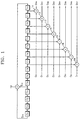
- Figure 1 is a circuit diagram of a random data generator which is used in a scrambler of a general DVD system, wherein an exclusive OR gate 10 and registers r 0 through r 14 for providing random data are referred to as a random data generator, and the random data generator and exclusive OR gates 11 through 18 are referred to as a scrambler.
- 15 bit registers r 0 through r 14 are shifted left in synchronization with the input of a clock signal to be scrambled.
- the input of the least significant register r 0 is a value obtained by performing an exclusive OR operation with respect to the outputs of the most significant register r 14 and the eleventh least significant register r 10 which are provided from the eXclusive OR (XOR) gate 10.
- the random data generation cycle in the random data generator shown in Figure 1 is 32K (kilobytes), and is consistent with the size of one Error Correction Code (ECC) block of a DVD, 32K. That is, in the ECC block, a random value having no periodicity is generated, a register is shifted left eight times, and then the XOR gates 11 through 18 perform XOR operations with respect to the outputs of eight lower registers r 0 through r 7 and input data D 0 through D 7 , whereby scrambled results are obtained.
- ECC Error Correction Code
- a data clock speed at which a data clock signal is input to the XOR gates 11 through 18 is 1/8 of a scramble clock speed at which a scramble clock signal is input to the registers r 0 through r 14 .
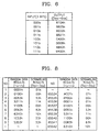
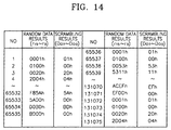
- Figure 2 is a table for showing the random data results of the registers r 0 through r 14 and scrambling results Do 0 through Do 7 when the initial values of the registers r 0 through r 14 shown in Figure 1 are set to be a hexadecimal number of "0001h” and input data D 0 through D 7 are "00h”. It can be seen from Figure 2 that the cycle of random data is 32K (32768).
- the values of the registers r 0 through r 14 are shifted left eight times, and then scrambling is performed. Accordingly, the registers r 0 through r 14 are initialized to initial values with reference to the four upper bits ID(7:4) within the last byte among a 4-byte identification code (ID) allocated to the head of a sector, which is a basic access unit. At this time, attention must be paid to select the initial values. That is, even if the same data is received, random data is generated from an initialized value within one sector, and values within the sector are equally repeated for a duration of 1 ECC block (16 sectors).
- ID 4-byte identification code
- an aim of embodiments of the present invention is to provide a random data generator having a serial structure, which can generate a large amount of data as random data.
- Another aim of embodiments is to provide a scrambler of a high-density optical disc system employing the random data generator having a serial structure.
- Still another aim of embodiments is to provide a random data generator having a parallel structure, which can generate a large amount of data as random data.
- Yet another aim is to provide a scrambler of a high-density optical disc system employing the random data generator having a parallel structure.
- a random data generator comprising: an m ⁇ n decoder for receiving m bits and outputting n bits; registers (r 0 -r n-1 ) arranged in series for shifting and storing the n bits; selection output circuits (m 0 -m n-1 ) for receiving n bits of output from the m ⁇ n decoder as selection signals, and providing "0" with respect to valid bits among the n bits of output from the m ⁇ n decoder and providing the outputs of the registers (r 0 -r n-1 )with respect to invalid bits; and logic circuits (G 0 -G n-1 ) for performing XOR operations with respect to the n bits of output from the selection output circuits (m 0 -m n-1 ) and the n bits of output from the registers (r 0 -r n-1 ), and feeding the results of the XOR operations back to a least significant register (r 0 ) only
- the m ⁇ n decoder outputs 2 m types of n bits with respect to the m input bits, thereby extending the cycle of the random data to 2 m times.
- the m ⁇ n decoder becomes a m ⁇ 16 decoder, and the cycle of the random data is 2 m ⁇ 64K.
- the m ⁇ n decoder may be a 3 ⁇ 8 decoder, and the cycle of random data is 8 ⁇ 64K.
- the m ⁇ n decoder may be a 1 ⁇ 2 decoder, and the cycle of random data is 2 ⁇ 64K.
- the number of effective branches of the outputs of the m ⁇ n decoder is preferably 4 or more.
- the number decoder is a 3X8 decoder having outputs (D o0 -D 015 ) and four effective branches
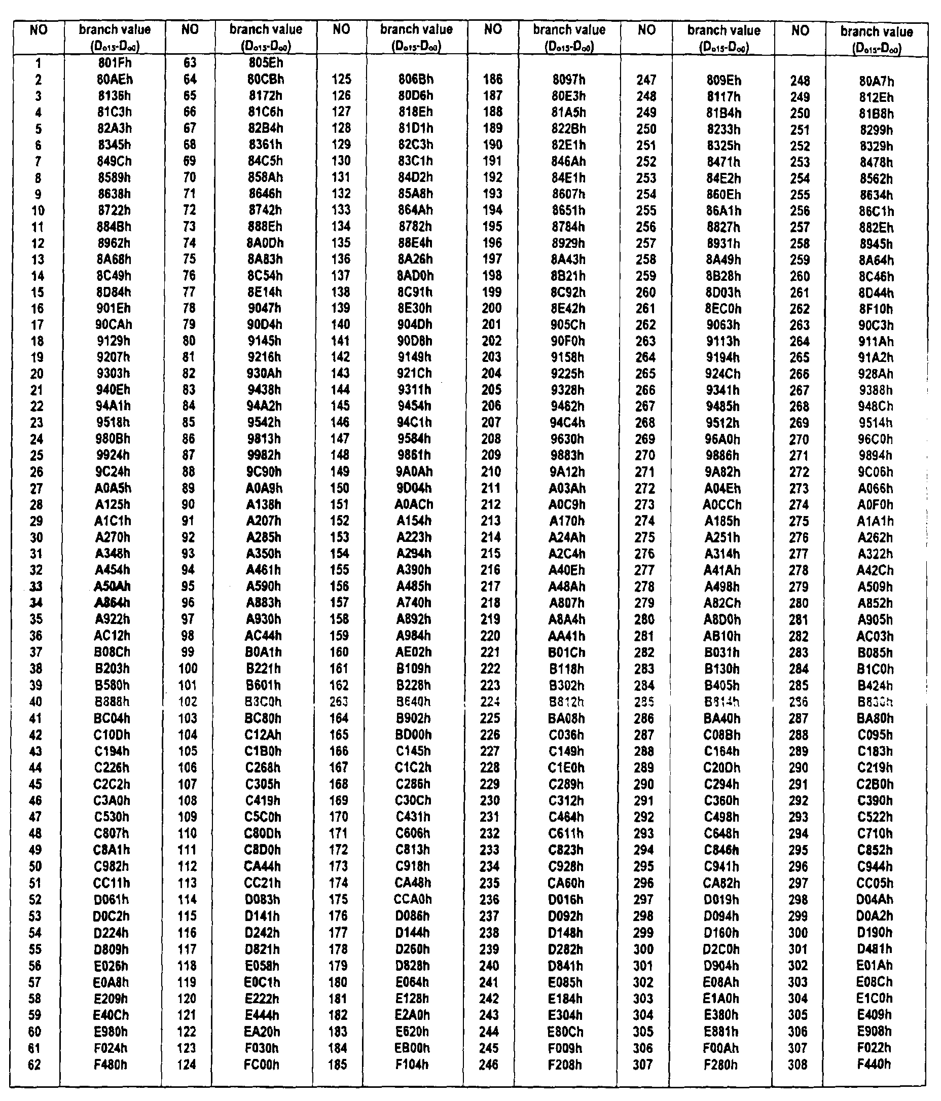
- the branch values related to the decoder outputs are as given in Figure 9 of the accompanying drawings.
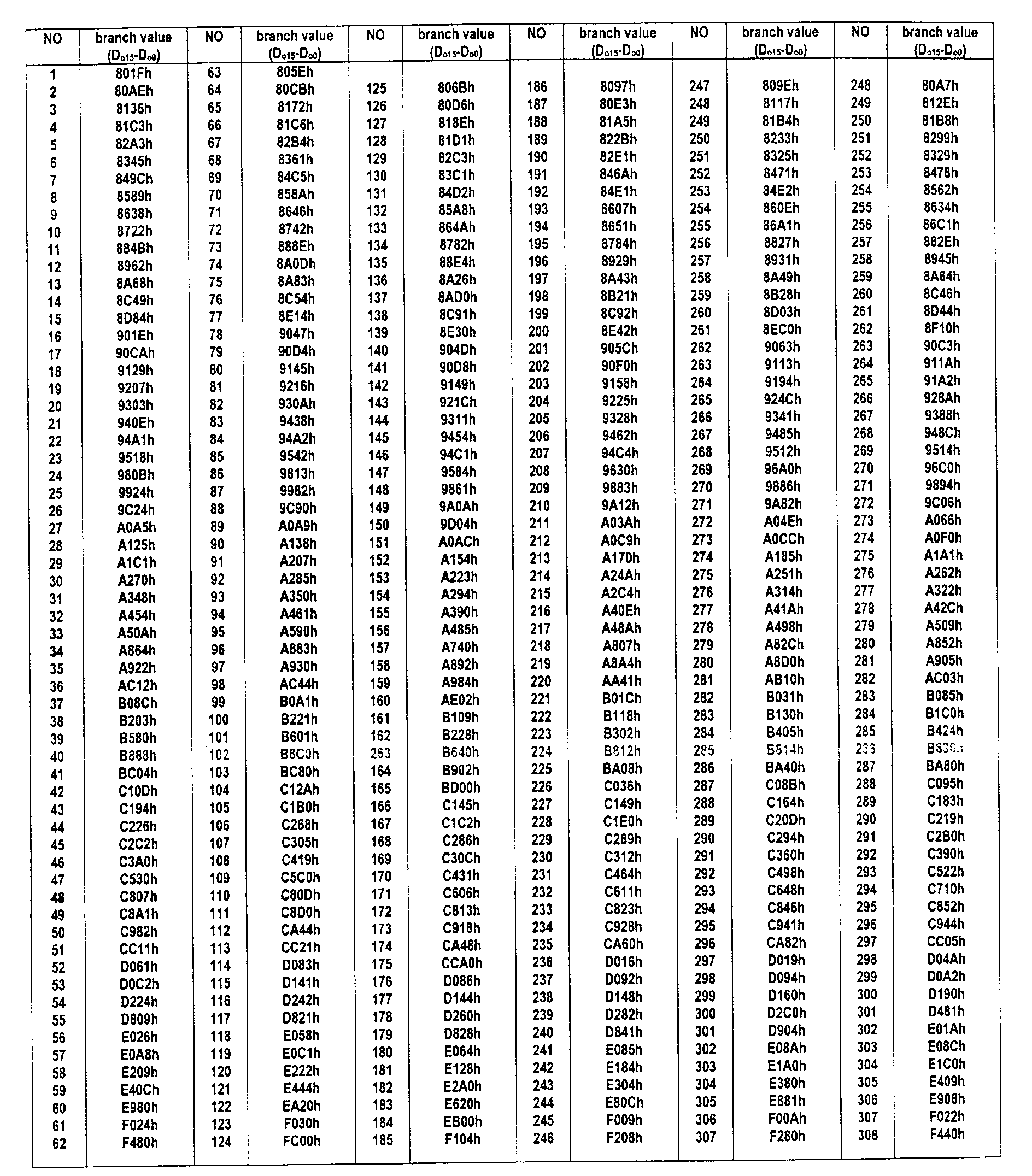
- the decoder is a 3x8 decoder having outputs (D o0 -D o15 ) and six effective branches the branch values related to the decoder outputs are preferably as given in Figure 10.
- the random data generator may be applied to a scrambler of an optical disc system, and the scrambler preferably comprises a random data generator and a predetermined number of logic gates for performing XOR operations with respect to input data and the outputs of as many lower registers as the predetermined number of logic gates to provide scrambling results.
- a random data generator comprising: n registers (r 0 -r n-1 ) arranged in series for shifting and storing n bits; logic circuits (G 0 -G n-1 ) arranged in series, which are realized with a plurality of logic gates, for performing XOR operations with respect to the outputs of the registers (r 0 -r n-1 ), which are valid corresponding to the number of logic gates having effective branches according to a predetermined branch value, and the outputs of adjacent logic gates, and feeding the results of the XOR operation back to a least significant register (r 0 ), wherein n bits of random data are generated from the registers.
- the number of effective branches is preferably 4 or more, and determined by the branch values shown in Figures 9 and 10.
- the random data generator is applied to a scrambler of an optical disc system
- the scrambler comprises a random data generator and a predetermined number of logic gates for performing XOR operations with respect to input data and the outputs of as many lower registers as the predetermined number of logic gates to provide scrambling results.
- a random data generator comprising: p logic circuits arranged in parallel, for receiving the outputs of n registers in parallel, performing XOR operations with respect to the outputs of the n registers which correspond to the results of n left-shifting operations having correspondence to the number of effective branches according to a predetermined branch value, and providing 2 m outputs; selection output circuits (m 0 -m 7 ), each for selecting one output among 2 m outputs provided from each of the logic circuits according to m-bit selection signals, and providing p outputs; and n registers (S 0 -S 7 ) arranged in parallel for generating random data, wherein (n-p) upper registers receive the outputs of p lower registers and the p lower registers receive the p outputs of the selection output circuit, wherein the outputs of registers (S 0 -S 7 ) corresponding to the number of effective branches having a predetermined branch value are fed back to the logic circuit.
- the cycle of random data provided from the registers is extended to 2 m times.
- the cycle of random data provided from the registers preferably becomes 2 m ⁇ 64K.
- the inputs (S o0 -S o15 ) of the p lower registers correspond to the values (D o0 -D o15 ) and have branch values as shown in Figure 9.
- the inputs (S o0 -S o15 ) of the p lower registers correspond to the values (D o0 -D o15 ) and have branch values shown in the Figure 10 table.
- the logic circuits are 8 ⁇ 2 3 XOR gates, and the selection output circuits select 8 outputs provided from the logic circuits using 3 bit selection signals and provide the selected data to 8 lower registers, while the remaining upper registers receive the outputs of the 8 lower registers.
- the random data generator is applied to a scrambler of an optical disc system
- the scrambler comprises a random data generator and a predetermined number of logic gates for performing XOR operations with respect to input data and the outputs of as many lower registers as the predetermined number of logic gates to provide scrambling results.
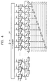
- Figure 4 is a circuit diagram of a random data generator having a serial structure according to the present invention and a scrambler using the random data generator.
- the random data generator includes an m ⁇ n decoder 100, n multiplexers m 0 through m n-1 , n XOR gates G 0 through G n-1 , and n registers r 0 through r n-1
- the scrambler includes the random data generator having such a configuration and XOR gates 101 through 108 for performing XOR operations with respect to input data D 0 through D 7 and the outputs of registers r 0 through r 7 to output the results of scrambling.
- the n multiplexers can be referred to as selection output circuits for selecting and outputting either "0" or the output of each register in response to the n-bit output of the m ⁇ n decoder 100, and the n XOR gates can be referred to as logic circuits for providing the n-bit results of XOR operations.
- the m ⁇ n decoder 100 receives m bits and outputs n bits.
- the n multiplexers m 0 through m n-1 receive n output bits Do 0 through Do n-1 as selection signals from the m ⁇ n decoder 100, and provide "0", received via a first input port A, as output signals Mo 0 through Mo n-1 to one side of each of the XOR gates G 0 through G n-1 when the values of the n-bit outputs Do 0 through Do n-1 of the m ⁇ n decoder 100 are "1".
- the XOR gates G 0 through G n-1 output the outputs S 0 through S n-1 of the registers r 0 through r n-1 received via the other sides thereof, without change, and finally the output of an accumulated XOR gate G 0 is fed back to the least significant register r 0 .
- the n multiplexers m 0 through m n-1 provide the outputs S 0 through S n-1 of the registers r 0 through r n-1 , received via the second input port B, as output signals Mo 0 through Mo n-1 to the XOR gates G 0 through G n-1 , when the values of the n output bits Do 0 through Do n-1 of the m ⁇ n decoder 100 are "0".
- the XOR gates G 0 through G n-1 perform XOR operations with respect to the outputs S 0 through S n-1 of the multiplexers m 0 through m n-1 and the outputs S 0 through S n-1 of the registers r 0 through r n-1 . Finally, the output of each of the XOR gates G 0 through G n-1 becomes "0", so there are no values to be fed back to the least significant register r 0 .
- n registers r 0 through r n-1 generate n-bit random data
- the XOR gates 101 through 108 provide the scrambling results of XOR operations performed on input data D 0 through D 7 and the outputs of the 8 lower registers r 0 through r 7 .
- Figure 5 is a circuit diagram of an embodiment of the random data generator and the scrambler using the same shown in Figure 4.
- the input to a 3 ⁇ 8 decoder 110 is set to be 3 bits, and the output therefrom is set to be 16 bits Do 0 through Do 15 which are classified into 8 types.
- An example of the outputs according to the inputs of the 3 ⁇ 8 decoder 110 is shown in Figure 6.
- the output value of the 3 ⁇ 8 decoder 110 is "CA00h” as shown in Figure 6. Accordingly, only the outputs Do 9 , Do 11 , Do 14 and Do 15 of the 3 ⁇ 8 decoder 110 are "1", so the outputs Mo 9 , Mo 11 , Mo 14 and Mo 15 of the multiplexers m 9 , m 11 , m 14 and m 15 become "0".
- the XOR gates G 9 , G 11 , G 14 and G 15 provide the outputs S 9 , S 11 , S 14 and S 15 of the corresponding registers r 9 , r 11 , r 14 and r 15 , received via the other side of each of the XOR gates G 9 , G 11 , G 14 and G 15 , as their outputs, so that the output values of the upper XOR gates G 9 , G 11 , G 14 and G 15 are valid.
- the outputs of the remaining multiplexers m 0 ,..., m 8 , m 10 , m 12 and m 13 are the outputs S 0 ,..., S 8 , S 10 , S 12 and S 13 of the registers r 0 ,..., r 8 , r 10 , r 12 and r 13 , so that the corresponding XOR gates G 0 ,..., G 8 , G 10 , G 12 and G 13 perform XOR operations with respect to the outputs S 0 ,..., S 8 , S 10 , S 12 and S 13 of the multiplexers m 0 , ..., m 8 , m 10 , m 12 and m 13 , each of which is received via one side of each of the corresponding XOR gates, and the outputs S 0 ,..., S 8 , S 10 , S 12 and S 13 of the registers r 0 , ..., r 8 , r 10 , r 12 and r
- the output Do 13 of the 3 ⁇ 8 decoder 110 is "0", so that the output S 13 of the register r 13 received via the second input port B is provided as its output Mo 13 .
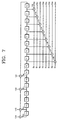
- the XOR gate G 13 performs a XOR operation with respect to the two data S 13 and S 13 and outputs "0", which means that the branches S 13 and Mo 13 of the XOR gate G 13 become invalid. Consequently, the random data generator and the scrambler using the same shown in Figure 5 can have the structure shown in Figure 7 if they are realized in a simple structure with respect to the output value "CA00h" of the 3 ⁇ 8 decoder 110.
- the valid branches of the XOR gates G 0 through G 15 in the random data generator vary with the outputs of the 3 ⁇ 8 decoder 110 shown in Figure 5, which changes the structure of the random data generator. Accordingly, generation of random data having a 8 ⁇ 64K cycle is enabled. This means that a random data generator for a long period can be realized with a structure of a type shown in Figure 5 without limit. If the values of the 3 ⁇ 8 decoder 110 capable of generating random data having a 64K cycle are arranged in the structure shown in Figure 5, tables of Figures 9 and 10 are obtained.
- Figure 9 is a table showing branch values in all possible cases, that is, the outputs Do 0 through Do 15 of the 3 ⁇ 8 decoder 110, when the number of XOR gates having effective branches of the XOR gates G 0 through G 15 in the random data generator shown in Figure 5 is four.
- Figure 10 is a table showing branch values in all possible cases, that is, the outputs Do 0 through Do 15 of the 3 ⁇ 8 decoder 110, when the number of XOR gates having effective branches of the XOR gates G 0 through G 15 in the random data generator shown in Figure 5 is six. There may be the cases that the number of effective branches is 8, 10 or 12.
- the cycle of random data is set to be 64K as an embodiment of the present invention, branch values capable of realizing this embodiment are proposed, and an m ⁇ n decoder is provided as shown in Figure 4 so as to extend the cycle of random data to 2 m ⁇ 64K.
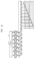
- FIG 11 A circuit diagram of another embodiment of the random data generator shown in Figure 4 and a scrambler using the random data generator is shown in Figure 11.
- Figure 11 intends to propose a device for generating random data having a long cycle, which has a hardware structure that is as simple as possible.
- the table shown in Figure 13 has random data extracted whenever the registers r 0 through r 15 are shifted left eight times, and indicates that one cycle is 64K (65536). Consequently, the results Do 0 through Do 7 obtained by scrambling the input data D 0 through D 7 become data intended to be finally used.
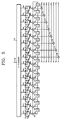
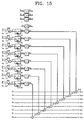
- Figure 15 shows a random data generator having a parallel structure according to the present invention and a scrambler using the random data generator.
- the structures of the random data generator and the scrambler are preferable for systems requiring high-speed signal processing.
- the results shifted left eight times are directly applied to each of the registers r 0 through r n-1 in parallel, so that the outputs S 0 through S n-1-8 of the registers r 0 through r n-1-8 are applied to upper registers r 8 through r n-1 .
- the input of the lower registers r 0 through r 7 depends on which branch structure is selected among the branch structures shown in Figure s 9 and 10. Also, the number of lower registers r 0 through r 7 shown is 8, but can vary with an input data bit (p).
- Multiplexers m 0 through m 7 each select one input among 2 m inputs provided via XOR gates 201 through 208 according to m-bit selection signals, and provide the selected input to corresponding registers r 0 through r 7 .
- the XOR gates 201 through 208 are a combination of several XOR gates.
- the outputs S 0 through S 7 of the registers r 0 through r 7 are input to the registers r 8 through r 15 arranged in parallel, respectively, and the results of (S 8 ⁇ S 7 ⁇ S 4 ⁇ S 2 ), (S 9 ⁇ S 8 ⁇ S 5 ⁇ S 3 ), (S 10 ⁇ S 9 ⁇ S 6 ⁇ S 4 ), (S 11 ⁇ S 10 ⁇ S 7 ⁇ S 5 ), (S 12 ⁇ S 11 ⁇ S 8 ⁇ S 6 ), (S 13 ⁇ S 12 ⁇ S 9 ⁇ S 7 ), (S 14 ⁇ S 13 ⁇ S 10 ⁇ S 8 ) and (S 15 ⁇ S 14 ⁇ S 11 ⁇ S 9 ) are applied to the registers r 0 through r 7 via the first input port A of each of the multiplexers m 0 through m 7 , respectively.
- the random data results provided from the registers r 0 through r 15 , and the scrambling results Do 0 through Do 7 when the input data D 0 through D 7 provided from the XOR gates 241 through 248 are "00b", are the same as those shown in a table of Figure 14.
- the serial structure shown in Figure 11 is simpler than a parallel structure, but may have a disadvantage in that it must operate fast.
- the parallel structure shown in Figure 16 operates at a speed of 1/8 of the operating speed of the serial structure, but may have a disadvantage in that the circuit is a little complicated. Thus, they can be selected according to the circumstances.
- random data having a cycle of 64K or greater can be generated, and a random data generator for 2 m ⁇ 64K can be realized with a m ⁇ n decoder.
- embodiments of the present invention can be used as a random data generator for a scrambler of a high-capacity optical disc system such as an anticipated high density (HD)-DVD.
Landscapes
- Engineering & Computer Science (AREA)
- Signal Processing (AREA)
- Theoretical Computer Science (AREA)
- Physics & Mathematics (AREA)
- General Physics & Mathematics (AREA)
- Computational Mathematics (AREA)
- Mathematical Optimization (AREA)
- Pure & Applied Mathematics (AREA)
- General Engineering & Computer Science (AREA)
- Mathematical Analysis (AREA)
- Signal Processing For Digital Recording And Reproducing (AREA)
- Dc Digital Transmission (AREA)
- Storage Device Security (AREA)
Abstract
Description
Claims (21)
- A random data generator comprising:a m×n decoder (100) for receiving m bits and outputting n bits;registers (r0-rn-1) arranged in series for shifting and storing the n bits;selection output circuits (m0-mn-1) for receiving n bits of output from the m×n decoder (100) as selection signals, and providing "0" with respect to valid bits among the n bits of output from the m×n decoder (100) and providing the outputs of the registers (r0-rn-1) with respect to invalid bits; andlogic circuits (G0-Gn-1) for performing XOR operations with respect to the n bits of output from the selection output circuits (m0-mn-1) and the n bits of output from the registers (r0-rn-1), and feeding the results of the XOR operations back to a least significant register (r0) only in the case of valid bits among the n bits of output from the m×n decoder (100),
wherein n bits of random data are generated from the registers (r0-rn-1). - The random data generator of claim 1, wherein the m×n decoder (100) outputs 2m types of n bits with respect to the m input bits, thereby extending the cycle of the random data to 2m times.
- The random data generator of claim 1, wherein when n in the m×n decoder (100) is set to be 16 and a predetermined branch value is selected, the cycle of the random data becomes 216 (=64K).
- The random data generator of claim 1, wherein, when m-bit selection signals are received and n is set to be 16, the m×n decoder (100) becomes a m×16 decoder, and the cycle of the random data is 2m×64K.
- The random data generator of claim 1, wherein the m×n decoder (100) is a 3×8 decoder, and the cycle of random data is 8×64K.
- The random data generator of claim 1, wherein the m×n decoder (100) is a 1×2 decoder, and the cycle of random data is 2×64K.
- The random data generator of claim 1, wherein the number of effective branches of the outputs of the m×n decoder is 4 or more.
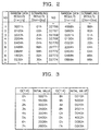
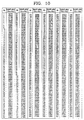
- The random data generator of claim 7, wherein when the number decoder is a 3x8 decoder (110) having outputs (Do0-Do15) and four effective branches the branch values related to the decoder outputs are as given in the table below:
NO BRANCH VALUE (Do15-Do0) NO BRANCH VALUE (Do15-Do0) 1 8016h 27 8940h 2 801Ch 28 8A04h 3 8029h 29 9028h 4 80D0h 30 9082h 5 810Ah 31 9120h 6 8112h 32 9420h 7 8112h 33 9840h 8 8142h 34 9C00h 9 8148h 35 A084h 10 8150h 36 A108h 11 8214H 37 A140h 12 8241H 38 A440h 13 8244H 39 A801h 14 8248H 40 A840h 15 8260H 41 B010h 16 8320H 42 B400h 17 8406H 43 C009h 18 8430H 44 C00Ah 19 8540H 45 C042h 20 8580H 46 C108h 21 8610H 47 C120h 22 8805H 48 C208h 23 8821H 49 C801h 24 8841H 50 CA00h 25 8842H 51 DA00h 26 8920H 52 D008h - The random generator of claim 7 wherein when the decoder is a 3x8 decoder (110) having outputs (Do0-Do15) and six effective branches, the branch values related to the decoder outputs being as given in the table below:
- The random data generator of any preceding claim, wherein the random data generator is applied to a scrambler of an optical disc system, and the scrambler comprises a random data generator and a predetermined number of logic gates for performing XOR operations with respect to input data and the outputs of as many lower registers as the predetermined number of logic gates to provide scrambling results.
- A random data generator comprising:n registers (r0-rn-1) arranged in series for shifting and storing n bits;logic circuits (G0-Gn-1) arranged in series, which are realized with a plurality of logic gates, for performing XOR operations with respect to the outputs of the registers (r0-rn-1), which are valid corresponding to the number of logic gates having effective branches according to a predetermined branch value, and the outputs of adjacent logic gates, and feeding the results of the XOR operation back to a least significant register (r0),
wherein n bits of random data are generated from the registers. - The random data generator of claim 11, wherein the number of effective branches is 4 or more, and it is determined by the branch values shown in Figures 9 and 10.
- The random data generator of claim 11, wherein when n is set to be 16, the cycle of the random data becomes 216 (=64K).
- The random data generator of claim 11, wherein the random data generator is applied to a scrambler of an optical disc system, and the scrambler comprises a random data generator and a predetermined number of logic gates for performing XOR operations with respect to input data and the outputs of as many lower registers as the predetermined number of logic gates to provide scrambling results.
- A random data generator comprising:p logic circuits (201-208) arranged in parallel, for receiving the outputs of n registers in parallel, performing XOR operations with respect to the outputs of the n registers which correspond to the results of n left-shifting operations having correspondence to the number of effective branches according to a predetermined branch value, and providing 2m outputs;selection output circuits (m0-m7), each for selecting one output among 2m outputs provided from each of the logic circuits according to m-bit selection signals, and providing p outputs; andn registers (S0-S7) arranged in parallel for generating random data, wherein (n-p) upper registers receive the outputs of p lower registers and the p lower registers receive the p outputs of the selection output circuit,
wherein the outputs of registers (S0-S7) corresponding to the number of effective branches having a predetermined branch value are fed back to the logic circuit. - The random data generator of claim 15, wherein the cycle of random data provided from the registers is extended to 2m times.
- The random data generator of claim 15, wherein when m-bit selection signals are received and n is set to be 16, the cycle of random data provided from the registers becomes 2m×64K.
- The random data generator of claim 15, wherein the inputs (So0-So15) of the p lower registers correspond to the values (Do0-Do15) and have branch values shown in the table below:
NO BRANCH VALUE (Do15-Do0) NO BRANCH VALUE (Do15-Do0) 1 8016h 27 8940h 2 801Ch 28 8A04h 3 8029h 29 9028h 4 80D0h 30 9082h 5 810Ah 31 9120h 6 8112h 32 9420h 7 8112h 33 9840h 8 8142h 34 9C00h 9 8148h 35 A084h 10 8150h 36 A108h 11 8214H 37 A140h 12 8241H 38 A440h 13 8244H 39 A801h 14 8248H 40 A840h 15 8260H 41 B010h 16 8320H 42 B400h 17 8406H 43 C009h 18 8430H 44 C00Ah 19 8540H 45 C042h 20 8580H 46 C108h 21 8610H 47 C120h 22 8805H 48 C208h 23 8821H 49 C801h 24 8841H 50 CA00h 25 8842H 51 DA00h 26 8920H 52 D008h - The random data generator of claim 15, wherein the inputs (So0-So15) of the p lower registers correspond to the values (Do0-Do15) and have branch values shown in the table below:
- The random data generator of claim 15, wherein the logic circuits are 8×23 XOR gates, and the selection output circuits select 8 outputs provided from the logic circuits using 3 bit selection signals and provide the selected data to 8 lower registers, while the remaining upper registers receive the outputs of the 8 lower registers.
- The random data generator of claim 15, wherein the random data generator is applied to a scrambler of an optical disc system, and the scrambler comprises a random data generator and a predetermined number of logic gates for performing XOR operations with respect to input data and the outputs of as many lower registers as the predetermined number of logic gates to provide scrambling results.
Applications Claiming Priority (2)
| Application Number | Priority Date | Filing Date | Title |
|---|---|---|---|
| KR1019990027886A KR100657240B1 (en) | 1999-07-10 | 1999-07-10 | Random data generator |
| KR9927886 | 1999-07-10 |
Publications (2)
| Publication Number | Publication Date |
|---|---|
| EP1069497A2 true EP1069497A2 (en) | 2001-01-17 |
| EP1069497A3 EP1069497A3 (en) | 2005-02-09 |
Family
ID=36688888
Family Applications (1)
| Application Number | Title | Priority Date | Filing Date |
|---|---|---|---|
| EP00305779A Withdrawn EP1069497A3 (en) | 1999-07-10 | 2000-07-07 | Pseudo-random data generator and scrambler using the same |
Country Status (5)
| Country | Link |
|---|---|
| US (1) | US7092979B1 (en) |
| EP (1) | EP1069497A3 (en) |
| JP (1) | JP2001075783A (en) |
| KR (1) | KR100657240B1 (en) |
| CN (2) | CN1755611A (en) |
Cited By (4)
| Publication number | Priority date | Publication date | Assignee | Title |
|---|---|---|---|---|
| GB2453259A (en) * | 2007-09-28 | 2009-04-01 | Intel Corp | Suppressing power supply noise using an LFSR pseudo random scrambling process |
| US8102996B2 (en) | 2004-12-01 | 2012-01-24 | Renesas Electronics Corporation | Scrambler, descrambler and method, and disc apparatus |
| US8503678B2 (en) | 2007-09-28 | 2013-08-06 | Intel Corporation | Suppressing power supply noise using data scrambling in double data rate memory systems |
| US9792246B2 (en) | 2014-12-27 | 2017-10-17 | Intel Corporation | Lower-power scrambling with improved signal integrity |
Families Citing this family (10)
| Publication number | Priority date | Publication date | Assignee | Title |
|---|---|---|---|---|
| KR100611955B1 (en) * | 1999-07-20 | 2006-08-11 | 삼성전자주식회사 | Scrambler |
| US7047262B2 (en) * | 2002-08-21 | 2006-05-16 | Koninklijke Philips Electronics N.V. | Entropy estimation and decimation for improving the randomness of true random number generation |
| KR100510492B1 (en) * | 2002-10-07 | 2005-08-26 | 삼성전자주식회사 | Word-wide scrambing/descrambling apparatus in optical disc system and Method there-of |
| JP4254201B2 (en) * | 2002-10-31 | 2009-04-15 | ソニー株式会社 | Scrambler, transmitter and receiver |
| TWI231655B (en) * | 2004-08-09 | 2005-04-21 | Univ Nat Central | Method for transforming serial scrambler to parallel scrambler, parallel scrambler and double edge-triggered register with XOR operation |
| JP5147412B2 (en) | 2005-01-21 | 2013-02-20 | サーティコム コーポレーション | Elliptic curve random number generation |
| CN101018097B (en) * | 2006-02-07 | 2011-09-21 | 华为技术有限公司 | Disturbance code generation device |
| CN101098299B (en) * | 2006-06-27 | 2010-08-18 | 中兴通讯股份有限公司 | Parallel method and device for bit scrambling |
| CN101022286B (en) * | 2007-03-20 | 2010-06-16 | 中兴通讯股份有限公司 | A bit scrambling parallel processing method and device |
| RU2331916C1 (en) * | 2007-06-21 | 2008-08-20 | Василий Георгиевич Архангельский | Random number generator |
Family Cites Families (18)
| Publication number | Priority date | Publication date | Assignee | Title |
|---|---|---|---|---|
| US4974184A (en) * | 1988-05-05 | 1990-11-27 | Honeywell Inc. | Maximum length pseudo-random test pattern generator via feedback network modification |
| US4959832A (en) * | 1988-12-09 | 1990-09-25 | International Business Machines | Parallel pseudorandom pattern generator with varying phase shift |
| JPH03214809A (en) * | 1990-01-19 | 1991-09-20 | Nec Corp | Linear feedback shift register |
| JPH0454720A (en) | 1990-06-25 | 1992-02-21 | Fujitsu Ltd | Serial pn pattern parallel generating circuit and constitution method for the circuit |
| JP2841882B2 (en) * | 1991-02-04 | 1998-12-24 | 日本電気株式会社 | Pseudo random pattern generator |
| JPH05260041A (en) * | 1992-03-10 | 1993-10-08 | Hitachi Ltd | Feedback shift type scramble pattern generation circuit |
| JPH0637603A (en) | 1992-07-16 | 1994-02-10 | Nec Corp | Maximum periodic system generating circuit |
| US5258936A (en) * | 1992-08-05 | 1993-11-02 | Motorola, Inc. | Method and apparatus for generating pseudo-random numbers |
| DE4234723A1 (en) | 1992-10-15 | 1994-04-21 | Philips Patentverwaltung | Arrangement for apparatus for recording and / or playing back digital video data |
| DE69433257T2 (en) * | 1993-07-20 | 2009-09-10 | Canon K.K. | Method and communication system using an encryption device |
| JPH07134647A (en) * | 1993-11-09 | 1995-05-23 | Matsushita Electric Ind Co Ltd | Random number generator |
| JPH0832416A (en) * | 1994-07-15 | 1996-02-02 | Ando Electric Co Ltd | Pseudo random pattern generating circuit |
| US5867409A (en) * | 1995-03-09 | 1999-02-02 | Kabushiki Kaisha Toshiba | Linear feedback shift register |
| DE69632243T2 (en) * | 1995-06-30 | 2005-01-13 | Sony Corp. | DATA RECORDING DEVICE AND METHOD, DATA RECORDING MEDIUM AND DATA PLAYING DEVICE AND METHOD |
| US5631962A (en) * | 1995-10-23 | 1997-05-20 | Motorola, Inc. | Circuit and method of encrypting key validation |
| KR100219631B1 (en) * | 1997-02-21 | 1999-09-01 | 윤종용 | Scrambler and descrambler |
| JPH11275052A (en) | 1998-03-19 | 1999-10-08 | Fujitsu Ltd | Spreading coding apparatus and method |
| KR100372226B1 (en) * | 2000-04-26 | 2003-02-14 | 휴먼일렉스(주) | Making process of amorphous metallic powder by high pressure water atomization |
-
1999
- 1999-07-10 KR KR1019990027886A patent/KR100657240B1/en not_active Expired - Fee Related
-
2000
- 2000-07-06 JP JP2000205799A patent/JP2001075783A/en active Pending
- 2000-07-07 EP EP00305779A patent/EP1069497A3/en not_active Withdrawn
- 2000-07-10 US US09/613,310 patent/US7092979B1/en not_active Expired - Fee Related
- 2000-07-10 CN CNA2005100927598A patent/CN1755611A/en active Pending
- 2000-07-10 CN CN00120451A patent/CN1280366A/en active Pending
Cited By (6)
| Publication number | Priority date | Publication date | Assignee | Title |
|---|---|---|---|---|
| US8102996B2 (en) | 2004-12-01 | 2012-01-24 | Renesas Electronics Corporation | Scrambler, descrambler and method, and disc apparatus |
| GB2453259A (en) * | 2007-09-28 | 2009-04-01 | Intel Corp | Suppressing power supply noise using an LFSR pseudo random scrambling process |
| GB2453259B (en) * | 2007-09-28 | 2010-02-10 | Intel Corp | Suppressing power supply noise |
| US7945050B2 (en) | 2007-09-28 | 2011-05-17 | Intel Corporation | Suppressing power supply noise using data scrambling in double data rate memory systems |
| US8503678B2 (en) | 2007-09-28 | 2013-08-06 | Intel Corporation | Suppressing power supply noise using data scrambling in double data rate memory systems |
| US9792246B2 (en) | 2014-12-27 | 2017-10-17 | Intel Corporation | Lower-power scrambling with improved signal integrity |
Also Published As
| Publication number | Publication date |
|---|---|
| EP1069497A3 (en) | 2005-02-09 |
| KR20010009500A (en) | 2001-02-05 |
| KR100657240B1 (en) | 2007-01-12 |
| JP2001075783A (en) | 2001-03-23 |
| CN1755611A (en) | 2006-04-05 |
| CN1280366A (en) | 2001-01-17 |
| US7092979B1 (en) | 2006-08-15 |
Similar Documents
| Publication | Publication Date | Title |
|---|---|---|
| US5917914A (en) | DVD data descrambler for host interface and MPEG interface | |
| EP1069497A2 (en) | Pseudo-random data generator and scrambler using the same | |
| KR100430697B1 (en) | Signal recording apparatus / signal reproducing apparatus and signal recording medium | |
| US4860353A (en) | Dynamic feedback arrangement scrambling technique keystream generator | |
| US5231662A (en) | Method and device for enciphering data to be transferred and for deciphering the enciphered data, and a computer system comprising such a device | |
| US20080056492A1 (en) | Copyright protective device and method | |
| JP3758231B2 (en) | Signal recording apparatus and method, and signal reproducing apparatus and method | |
| US8001391B2 (en) | Method of encrypting and decrypting data stored on a storage device using an embedded encryption/decryption means | |
| KR100630035B1 (en) | Information recording medium,and method and apparatus for recording and reproducing information using the same | |
| US5408531A (en) | Information recording/reproducing apparatus for converting and processing data exceeding error correction ability at recording | |
| US7058178B2 (en) | Synchronous stream cipher | |
| US5987630A (en) | Method of descrambling scrambled data using a scramble pattern and scramble pattern generator | |
| JP4202658B2 (en) | Data writing apparatus and DVD format data generation method | |
| US20080250306A1 (en) | Coding circuit for recording data on dvd disk | |
| KR20010071254A (en) | A method and system for providing copy-protection on a storage medium and storage medium for use in such a system | |
| US20070098160A1 (en) | SCRAMBLING AND SELF-SYNCHRONIZING DESCRAMBLING METHODS FOR BINARY AND NON-BINARY DIGITAL SIGNALS NOT USING LFSRs | |
| US7277545B1 (en) | Scrambler and scrambling method | |
| US20090080665A1 (en) | Method of Generating Secure Codes for a Randomized Scrambling Scheme for the Protection of Unprotected Transient Information | |
| JP2001184787A (en) | Information recording medium, information recording / reproducing device, and information recording / reproducing method | |
| US5856798A (en) | Magnetic-tape recording/reproducing arrangement comprising a coding device | |
| US6912661B1 (en) | Method and apparatus for encrypting and for decrypting data arranged in a data sector | |
| KR100611973B1 (en) | Scramble method | |
| NL9001296A (en) | TELETEXT DECODER, AND AN ERROR DETECTION AND CORRECTION CIRCUIT. | |
| KR100611974B1 (en) | Record / playback device |
Legal Events
| Date | Code | Title | Description |
|---|---|---|---|
| PUAI | Public reference made under article 153(3) epc to a published international application that has entered the european phase |
Free format text: ORIGINAL CODE: 0009012 |
|
| 17P | Request for examination filed |
Effective date: 20000727 |
|
| AK | Designated contracting states |
Kind code of ref document: A2 Designated state(s): AT BE CH CY DE DK ES FI FR GB GR IE IT LI LU MC NL PT SE |
|
| AX | Request for extension of the european patent |
Free format text: AL;LT;LV;MK;RO;SI |
|
| PUAL | Search report despatched |
Free format text: ORIGINAL CODE: 0009013 |
|
| AK | Designated contracting states |
Kind code of ref document: A3 Designated state(s): AT BE CH CY DE DK ES FI FR GB GR IE IT LI LU MC NL PT SE |
|
| AX | Request for extension of the european patent |
Extension state: AL LT LV MK RO SI |
|
| AKX | Designation fees paid |
Designated state(s): DE FR GB NL |
|
| 17Q | First examination report despatched |
Effective date: 20061013 |
|
| STAA | Information on the status of an ep patent application or granted ep patent |
Free format text: STATUS: THE APPLICATION IS DEEMED TO BE WITHDRAWN |
|
| 18D | Application deemed to be withdrawn |
Effective date: 20080409 |