EP1069464A2 - Reflection type liquid crystal display device - Google Patents
Reflection type liquid crystal display device Download PDFInfo
- Publication number
- EP1069464A2 EP1069464A2 EP00305880A EP00305880A EP1069464A2 EP 1069464 A2 EP1069464 A2 EP 1069464A2 EP 00305880 A EP00305880 A EP 00305880A EP 00305880 A EP00305880 A EP 00305880A EP 1069464 A2 EP1069464 A2 EP 1069464A2
- Authority
- EP
- European Patent Office
- Prior art keywords
- signal line
- gate
- liquid crystal
- insulating film
- electrode
- Prior art date
- Legal status (The legal status is an assumption and is not a legal conclusion. Google has not performed a legal analysis and makes no representation as to the accuracy of the status listed.)
- Withdrawn
Links
Images


Classifications
-
- G—PHYSICS
- G02—OPTICS
- G02F—OPTICAL DEVICES OR ARRANGEMENTS FOR THE CONTROL OF LIGHT BY MODIFICATION OF THE OPTICAL PROPERTIES OF THE MEDIA OF THE ELEMENTS INVOLVED THEREIN; NON-LINEAR OPTICS; FREQUENCY-CHANGING OF LIGHT; OPTICAL LOGIC ELEMENTS; OPTICAL ANALOGUE/DIGITAL CONVERTERS
- G02F1/00—Devices or arrangements for the control of the intensity, colour, phase, polarisation or direction of light arriving from an independent light source, e.g. switching, gating or modulating; Non-linear optics
- G02F1/01—Devices or arrangements for the control of the intensity, colour, phase, polarisation or direction of light arriving from an independent light source, e.g. switching, gating or modulating; Non-linear optics for the control of the intensity, phase, polarisation or colour
- G02F1/13—Devices or arrangements for the control of the intensity, colour, phase, polarisation or direction of light arriving from an independent light source, e.g. switching, gating or modulating; Non-linear optics for the control of the intensity, phase, polarisation or colour based on liquid crystals, e.g. single liquid crystal display cells
- G02F1/133—Constructional arrangements; Operation of liquid crystal cells; Circuit arrangements
- G02F1/136—Liquid crystal cells structurally associated with a semi-conducting layer or substrate, e.g. cells forming part of an integrated circuit
- G02F1/1362—Active matrix addressed cells
- G02F1/136227—Through-hole connection of the pixel electrode to the active element through an insulation layer
-
- G—PHYSICS
- G02—OPTICS
- G02F—OPTICAL DEVICES OR ARRANGEMENTS FOR THE CONTROL OF LIGHT BY MODIFICATION OF THE OPTICAL PROPERTIES OF THE MEDIA OF THE ELEMENTS INVOLVED THEREIN; NON-LINEAR OPTICS; FREQUENCY-CHANGING OF LIGHT; OPTICAL LOGIC ELEMENTS; OPTICAL ANALOGUE/DIGITAL CONVERTERS
- G02F1/00—Devices or arrangements for the control of the intensity, colour, phase, polarisation or direction of light arriving from an independent light source, e.g. switching, gating or modulating; Non-linear optics
- G02F1/01—Devices or arrangements for the control of the intensity, colour, phase, polarisation or direction of light arriving from an independent light source, e.g. switching, gating or modulating; Non-linear optics for the control of the intensity, phase, polarisation or colour
- G02F1/13—Devices or arrangements for the control of the intensity, colour, phase, polarisation or direction of light arriving from an independent light source, e.g. switching, gating or modulating; Non-linear optics for the control of the intensity, phase, polarisation or colour based on liquid crystals, e.g. single liquid crystal display cells
- G02F1/133—Constructional arrangements; Operation of liquid crystal cells; Circuit arrangements
- G02F1/1333—Constructional arrangements; Manufacturing methods
- G02F1/1335—Structural association of cells with optical devices, e.g. polarisers or reflectors
- G02F1/133553—Reflecting elements
-
- G—PHYSICS
- G02—OPTICS
- G02F—OPTICAL DEVICES OR ARRANGEMENTS FOR THE CONTROL OF LIGHT BY MODIFICATION OF THE OPTICAL PROPERTIES OF THE MEDIA OF THE ELEMENTS INVOLVED THEREIN; NON-LINEAR OPTICS; FREQUENCY-CHANGING OF LIGHT; OPTICAL LOGIC ELEMENTS; OPTICAL ANALOGUE/DIGITAL CONVERTERS
- G02F2203/00—Function characteristic
- G02F2203/02—Function characteristic reflective
Definitions
- the present invention relates to a reflection type liquid crystal display device of a normally white mode, which employs a thin film transistor (referred to hereinafter as TFT) and a reflective display electrode connected to the TFT.
- TFT thin film transistor
- a reflection type liquid crystal display device of a normally white mode using a conventional TFT is described below.
- a "normally" white mode refers to the liquid crystal orientation mode in which light is transmitted when no voltage is applied to the liquid crystal.
- a reflection type liquid crystal display device is a display device in which an image is displayed by reflecting incident light from the observer side with a reflective display electrode.
- Fig. 1 is a plan view showing an area around a display pixel region in a conventional reflection type liquid crystal display device.
- Fig. 2 is a cross-sectional view taken along line B-B in Fig. 1.
- a gate signal line 51 which includes gate electrodes 11 in portions thereof is provided for supplying a gate signal to a gate.
- a drain signal line (data signal line) 52 which includes drain electrodes 16 in portions thereof is provided for supplying a drain signal to a drain.
- a TFT is provided near an intersection of the gate signal line and the drain signal line. In the TFT, the gate 11 is connected to the gate signal line 51, the drain 13d is connected to the drain signal line 52, and the source 13s is connected to a reflective display electrode 20.
- first gate electrodes 11 composed of a refractory metal such as Cr or Mo
- gate insulating film 12 composed of an SiN film and SiO 2 film
- active layer 13 formed with poly-silicon film in discrete island patterns.
- the active layer 13 includes channels 13c provided above the first gate electrodes 11.
- the active layer 13 further includes a source 13s and a drain 113d formed by ion doping on the respective sides of the channels 13c.
- a stopper insulating film 14 made of SiO 2 film is provided over the channels 13c to function as the mask covering the channels 13c such that ions do not enter into the channels 13c during ion doping.
- an interlayer insulating film 15 is formed on the entire surface over the gate insulating film 12, the active layer 13, and the stopper insulating film 14, by sequential lamination of a SiO 2 film, a SiN film, and a SiO 2 film.
- a contact hole formed in the interlayer insulating film 15 in a position corresponding to the drain 13d is filled with metal using Al only, or by sequentially depositing Mo and Al, to thereby form a drain electrode 16.
- the drain signal line 52 is disposed on the interlayer insulating film 15. Furthermore, a planarizing insulating film 19 made of a material such as an organic resin is provided on the entire surface.
- a contact hole is formed in the planarizing insulating film 19 in a position corresponding to the source 13s.
- a reflective display electrode 20 that contacts the source 13s through this contact hole is formed using a reflective and conductive material such as Al.
- the reflective display electrode 20 simultaneously serves as a source electrode.
- An alignment layer 21 for orienting the liquid crystal 36 is provided further on top.
- a counter electrode substrate 30 has, on the side facing the insulator substrate 10 and the liquid crystal 36, color filters 31 for each of red (R), green (G), and blue (B), a counter electrode 32, and an alignment layer 33.
- color filters 31 for each of red (R), green (G), and blue (B) are provided on the other side of the substrate 30.
- a retardation film 34 and a polarizer 35 are provided on the other side of the substrate 30.
- the insulator substrate 10 provided with TFTs in the above-described manner and the counter electrode substrate 30 are sealed by surrounding the substrates with a sealing adhesive. The gap created between the two substrates is then filled with liquid crystal 36 to complete the liquid crystal display device.
- the reflective display electrodes 20 are arranged such that the gaps between adjacent electrodes 20 lie above the gate signal lines 51 and the drain signal lines 52, as shown in Fig. 1.
- a gap between adjacent reflective display electrodes 20 is arranged above the drain signal line 52.
- incident light 101 from a light source transmits through the polarizer 35, the retardation film 34, the counter electrode substrate 30, the alignment layer 33, the liquid crystal 36, the alignment layer 21, and the planarizing insulating film 19 to reach the drain signal line 52.
- the incident light 101 is then reflected by the drain signal line 52 through a reverse path, namely, the path indicated by a dotted line 102, to radiate out of the polarizer 35. More specifically, incident light 101 entering through the above-mentioned path is reflected by the drain signal line 52 composed of Al having a reflectance of approximately 95% or more, and reflected light 102 is therefore constantly observed by the observer 100.
- a conventional reflective liquid crystal display device of a normally white mode is disadvantageous in that, even when a black image is displayed, the reflected light 102 generates display defects in the form of white lines along the drain signal lines 52, thereby decreasing contrast.
- a further disadvantage is that the aperture ratio is small because the reflective display electrodes 20 are not formed in areas in which the TFTs are provided.
- the present invention was created in light of the above problems.
- the purpose of the present invention is to provide a reflection type liquid crystal display device of a normally white mode having a high aperture ratio, in which generation of display defects due to reflection of incident light by signal lines is prevented when a black image is displayed on the device.
- the reflection type liquid crystal display device is a reflection type liquid crystal display device of a normally white mode comprising a substrate having a gate signal line and a data signal line arranged to intersect one another, and a plurality of display pixel regions defined by the gate signal line and the data signal line.
- Each display pixel region includes a thin film transistor connected to the gate signal line and the data signal line, and a reflective display electrode connected to the thin film transistor.
- the reflective display electrode covers an area in which the thin film transistor is formed, and extends into an adjacent display pixel region located beyond the gate signal line.
- a gap between the reflective display electrodes in the display pixel regions located adjacent to one another on either side of the gate signal line is positioned in an offset arrangement from the position in which the gate signal line is formed.
- the reflection type liquid crystal display device is a reflection type liquid crystal display device of a normally white mode comprising a substrate having a gate signal line and a data signal line arranged to intersect one another, and a plurality of display pixel regions defined by the gate signal line and the data signal line, each display pixel region including a thin film transistor connected to the gate signal line and the data signal line, and a reflective display electrode connected to the thin film transistor, wherein the reflective display electrode covers an area in which the thin film transistor is formed, and extends into an adjacent display pixel region located beyond the data signal line.
- a gap between the reflective display electrodes in the display pixel regions located adjacent to one another on either side of the data signal line is positioned in an offset arrangement from the position in which the data signal line is formed.
- the reflective display electrode covers an area in which the thin film transistor is formed, and extends into an adjacent display pixel region located beyond the gate signal line, while a gap between the reflective display electrodes in the display pixel regions located adjacent to one another on either side of the gate signal line is positioned in an offset arrangement from the position in which the gate signal line is formed, and, at the same time, the reflective display electrode also extends into an adjacent display pixel region located beyond the data signal line.
- the gap between the reflective display electrodes in the display pixel regions located adjacent to one another on either side of the data signal line is positioned in an offset arrangement from the position in which the data signal line is formed.
- the thin film transistor comprises a first gate electrode constituting an integral portion of the gate signal line, a semiconductor film including a first insulating film, a channel, a source, and a drain, and a second insulating film. On the second insulating film, a second gate electrode is formed so as to cover the area over the channel.
- the second gate electrode is connected to the first gate electrode.
- the thin film transistor comprises a plurality of first gate electrodes constituting integral portions of the gate signal line, a first insulating film, a semiconductor film extending so as to intersect said plurality of first gate electrodes and including channels formed in positions overlapping each of said plurality of first gate electrodes, a second insulating film, and a second gate electrodes formed on the second insulating film so as to cover over an area in which the channel is formed.
- a gap between reflective display electrodes in adjacent display pixel regions is positioned in an offset arrangement from the position of a gate signal line and/or data line which is often composed of a conductive material having a high reflectance.
- a reflection type display device having high contrast and a high aperture rate can be achieved.
- the thin film transistor by configuring the thin film transistor with a first gate electrode and a second gate electrode sandwiching a semiconductor film having insulating films and a channel, influence of the electric field generated by reflective display electrode for the channel can be reliably prevented, accomplishing a display device having minimal fluctuation in the characteristics of the thin film transistors.
- the width of the second gate electrode in the channel length direction is made narrower than the width of the first gate electrode in the same channel length direction.
- Fig. 1 is a plan view showing an area around a display pixel region of a conventional reflection type liquid crystal display device.
- Fig. 2 is a cross-sectional view showing an area around a display pixel region of the conventional reflection type liquid crystal display device.
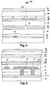
- Fig. 3 is a plan view showing an area around a display pixel region of a reflection type liquid crystal display device according to a preferred embodiment of the present invention.
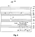
- Fig. 4 is a cross-sectional view showing an area around a display pixel region of a reflection type liquid crystal display device according to the preferred embodiment of the present invention.
- Fig. 5 is another cross-sectional view showing an area around a display pixel region of a reflection type liquid crystal display device according to the preferred embodiment of the present invention.
- Fig. 6 is a further cross-sectional view showing an area around a display pixel region of a reflection type liquid crystal display device according to the preferred embodiment of the present invention.
- Fig. 3 is a plan view showing an area around a display pixel region of a reflection type liquid crystal display device according to the embodiment of the present invention.
- Fig. 4 is a cross-sectional view of the liquid crystal display device taken along line A-A in Fig. 3.
- Fig. 5 is a cross-sectional view taken along line B-B in Fig. 3.
- Fig. 6 is a cross-sectional view of the reflection type liquid crystal display device taken along line C-C in Fig. 3.
- a TFT is disposed near an intersection of a gate signal line 51 including first gate electrodes 11 in portions thereof and a drain signal line 52 including drain electrodes 16 in portions thereof.
- the TFT is connected to a reflective display electrode 20 composed of a reflective material.
- the reflective display electrode 20 is arranged to extend over the TFT, as indicated by dotted lines in Fig. 3.
- first gate electrodes 11 composed of a refractory metal such as Cr or Mo
- gate insulating film 12 composed of an SiN film and SiO 2 film
- active layer 13 formed using a poly-silicon film.
- the active layer 13 includes channels 13c provided above the first gate electrodes 11.
- the active layer 13 further includes a source 13s and a drain 113d formed by ion doping on the respective sides of the channels 13c.
- a stopper insulating film 14 made of an SiO 2 film is provided over the channels 13c to function as the mask covering the channels 13c such that ions do not enter into the channels 13c during the ion doping for forming the source 13s and the drain 13d.
- an interlayer insulating film 15 is formed on the entire surface over the gate insulating film 12, the active layer 13, and the stopper insulating film 14.
- the interlayer insulating film 15 may be a single material organic film composed of an organic material such as SiO 2 , SiN, or acrylic material, or alternatively, a multi-layer composed of a combination of any of those materials.
- a contact hole formed in the interlayer insulating film 15 in a position corresponding to the drain 13d is filled with metal by using Al only or by sequentially depositing Mo and Al, to thereby form a drain electrode 16.
- second gate electrodes 17 are formed on the interlayer insulating film 15 in the position above the channels 13c.
- metal second gate electrodes 17 formed using Al only or using a sequential deposit of Mo and Al are provided.
- the second gate electrodes 17 disposed on the interlayer insulating film 15 are connected to the gate signal wiring line 51 on the insulator substrate 10 via a contact hole 18 created in the gate insulating film 12 and the interlayer insulating film 15.
- the drain signal line 52 is disposed on the interlayer insulating film 15.
- a planarizing insulating film 19 made of a material such as an organic resin is provided on the entire surface.
- a contact hole is formed in the planarizing insulating film 19 in a position corresponding to the source 13s.
- a reflective display electrode 20 that contacts the source 13s through this contact hole is formed using a reflective and conductive material such as Al.
- the reflective display electrode 20 simultaneously serves as a source electrode.
- An alignment layer 21 for orienting the liquid crystal 36 is provided further on top.
- the insulator substrate 10 provided with TFTs in the above-described manner and the counter electrode substrate 30 having a counter electrode 30 and an alignment layer 32 facing the insulator substrate 10 are sealed by surrounding the substrates with a sealing adhesive.
- the gap created between the two substrates is then filled with liquid crystal 36 to complete the liquid crystal display device.
- the reflective display electrode 20 formed on the planarizing insulating film 19 is next described in detail.
- the reflective display electrodes 20 are disposed as shown in Figs. 3 and 4.
- the gap (space) 37 between the reflective display electrodes 20 is prevented from overlapping the drain signal line 52 by being shifted from the position in which the signal line 52 is formed.
- the incident light 101 originating from the side of the observer 100 transmits through the polarizer 35, retardation film 34, the counter electrode substrate 30, the alignment layer 33, the liquid crystal 36, and the alignment layer 21, to pass through the gap 37.
- the transmitted light thus reaches the planarizing insulating film 19 and the interlayer insulating film 15.
- the incident light 101 from the observer 100 side irradiates the insulating films after passing through the layers and the gap 37.
- the insulating films have a reflectance of 1% or less, the incident light 101 is almost completely absorbed and is not reflected back to the observer 100.
- the gap 37 between the reflective display electrodes 20 is prevented from being positioned above the gate signal line 51.
- the gap 37 is arranged such that the gate electrode 51, which would reflect the incident light 101, is not located under the gap 37, and only the planarizing insulating film 19 and the interlayer insulating film 15 are positioned below the gap 37.
- the incident light 101 is prevented from being reflected by the gate signal line 51 as occurs in a conventional device. Even when a black image is displayed on the reflection type liquid crystal display device of a normally white mode, no white lines are visible along the signal line no incident light is reflected by the signal line.
- the incident light 101 from the observer 100 side is prevented from being reflected by the signal lines 51,52, such that the reflected light 102 is not visible to the observer 100.
- the reflection type liquid crystal display device of a normally white mode display defects in the form of white lines along the signal lines are not generated.
- a second gate electrode 17 is positioned over a channel 13c and connected to a first gate electrode 11, and a reflective display electrode 20 extends over the TFT, adhesion of impurities to the surface of the interlayer insulating film can be prevented. This in turn prevents accumulation of electric charges on the surface of the interlayer insulating film, allowing fabrication of TFTs having a stable threshold voltage. In this way, defects such as bright spots can be reduced, and a display image having a uniform luminance over the entire screen can be achieved. Furthermore, a liquid crystal display device having a high aperture rate can be accomplished.
- the gap 37 between the reflective display electrodes 20 is prevented from overlapping each of the gate signal line 51 and the drain signal line 52 in the present embodiment, the gap 37 may also be arranged to avoid overlapping only one of the gate signal line 51 and the drain signal line 52. Preferably, the gap 37 is positioned over neither of the signal lines 51,52.
- a reflective display electrode 20 extends into adjacent display pixel regions. Adjacent display pixel regions are defined as the display pixel regions surrounding one particular display pixel region in the vertical, horizontal, and diagonal directions.
- a reflective display electrode 20 overlaps a gate signal line as shown in Fig. 3, from among the nth and n+1th gate signal lines 51 adjacently located on the upper and lower sides, the reflective display electrode 20 preferably overlaps the gate signal line for the subsequent n+1th row, rather than the nth gate signal line to which the electrode 20 is connected.
- gate signal lines are sequentially selected from the ones located near the top of the screen (in the order of n-1th, nth, and n+1th) to be applied with a gate voltage.
- a display signal voltage is applied to each of the reflective display electrodes connected to the nth gate signal line when the nth gate signal line is selected. Accordingly, if the nth gate signal line and a corresponding reflective display electrode 20 are positioned in an overlap, there is a possibility that the application of the display signal to the electrode 20 becomes deficient. However, this problem is avoided if the electrode 20 corresponding to the nth gate signal line overlaps the n+1th gate signal line because, when the display signal voltage is applied to the electrode 20, no gate voltage is applied to the n+1th gate signal line.
- the second gate electrode 17 is disposed on the interlayer insulating film 15.
- the width of the second gate electrode 17 is smaller than the channel length of each channel 13c and the width of the gate electrode 11, such that the second gate electrode 17 does not overlap the end portions of the channel 13c and the gate electrode 11.
- the present invention may be configured such that the width of the second gate electrode 17 is wider than the width of the gate electrode 11.
- both of the first gate electrodes 11 may be covered with the second gate electrodes 17.
- the second gate electrode 17 may be disposed on only one of the first gate electrodes 11.
- each of the insulating films provided between the second gate electrode 17 and the active layer 13, which may be the stopper insulating film 14, the interlayer insulating film 15, and the planarizing insulating film 19 of the present embodiment may be composed of a single material film such as an SiO 2 film, an SiN film, or an organic film, or alternatively, composed of a lamination of those films.
- the TFT structure may also be a single gate structure including one gate, or a multi-gate structure including three or more gates.
Landscapes
- Physics & Mathematics (AREA)
- Nonlinear Science (AREA)
- Mathematical Physics (AREA)
- Chemical & Material Sciences (AREA)
- Crystallography & Structural Chemistry (AREA)
- General Physics & Mathematics (AREA)
- Optics & Photonics (AREA)
- Engineering & Computer Science (AREA)
- Microelectronics & Electronic Packaging (AREA)
- Liquid Crystal (AREA)
- Thin Film Transistor (AREA)
Abstract
Description
Claims (7)
- A reflection type liquid crystal display device of a normally white mode, having a substrate provided with a gate signal line and a data signal line arranged to intersect one another, and a plurality of display pixel regions defined by the gate signal line and the data signal line, each of the plurality of display pixel regions including:a thin film transistor connected to said gate signal line and said data signal line; anda reflective display electrode connected to said thin film transistor; whereinsaid reflective display electrode covers an area in which said thin film transistor is formed, and extends into an adjacent display pixel region located beyond said gate signal line; anda gap between the reflective display electrodes in the display pixel regions located adjacent to one another on either side of said gate signal line is positioned in an offset arrangement from a position in which said gate signal line is formed.
- A reflection type liquid crystal display device as defined in Claim 1, whereinsaid reflective display electrode extends into an adjacent display pixel region located beyond said data signal line; anda gap between the reflective display electrodes in the display pixel regions located adjacent to one another on either side of said data signal line is positioned in an offset arrangement from a position in which said data signal line is formed.
- A reflection type liquid crystal display device of a normally white mode, having a substrate provided with a gate signal line and a data signal line arranged to intersect one another, and a plurality of display pixel regions defined by the gate signal line and the data signal line, each of the plurality of display pixel regions including:a thin film transistor connected to said gate signal line and said data signal line; anda reflective display electrode connected to said thin film transistor; whereinsaid reflective display electrode covers an area in which said thin film transistor is formed, and extends into an adjacent display pixel region located beyond said data signal line; anda gap between the reflective display electrodes in the display pixel regions located adjacent to one another on either side of said data signal line is positioned in an offset arrangement from a position in which said data signal line is formed.
- A reflection type liquid crystal display device as defined in any one of Claims 1 to 3, whereinsaid thin film transistor comprises:a first gate electrode constituting an integral portion of said gate signal line;a semiconductor film including a first insulating film, a channel, a source, and a drain;a second insulating film; anda second gate electrode formed on said second insulating film so as to cover an area over said channel.
- A reflection type liquid crystal display device as defined in any one of Claims 1 to 3, whereinsaid thin film transistor comprises:a plurality of first gate electrodes constituting integral portions of said gate signal line;a first insulating film;a semiconductor film extending so as to intersect said plurality of first gate electrodes and including channels formed in positions overlapping each of said plurality of first gate electrodes;a second insulating film; anda second gate electrode formed on said second insulating film so as to cover an area over said channel.
- A reflection type liquid crystal display device as defined in Claim 4 or 5, wherein
said second gate electrode is connected to said first gate electrode. - A reflection type liquid crystal display device as defined in any one of Claims 4 to 6, wherein
a width of said second gate electrode in a channel length direction is narrower than a width of said first gate electrode in the channel length direction.
Applications Claiming Priority (2)
| Application Number | Priority Date | Filing Date | Title |
|---|---|---|---|
| JP20059899 | 1999-07-14 | ||
| JP20059899 | 1999-07-14 |
Publications (2)
| Publication Number | Publication Date |
|---|---|
| EP1069464A2 true EP1069464A2 (en) | 2001-01-17 |
| EP1069464A3 EP1069464A3 (en) | 2004-02-04 |
Family
ID=16427031
Family Applications (1)
| Application Number | Title | Priority Date | Filing Date |
|---|---|---|---|
| EP00305880A Withdrawn EP1069464A3 (en) | 1999-07-14 | 2000-07-12 | Reflection type liquid crystal display device |
Country Status (4)
| Country | Link |
|---|---|
| US (1) | US6504593B1 (en) |
| EP (1) | EP1069464A3 (en) |
| KR (1) | KR100400624B1 (en) |
| TW (1) | TW526355B (en) |
Cited By (2)
| Publication number | Priority date | Publication date | Assignee | Title |
|---|---|---|---|---|
| GB2362509A (en) * | 1999-11-16 | 2001-11-21 | Nec Corp | Thin film transistor (TFT) with front and back channel gates connected together |
| US7256850B2 (en) | 2000-09-25 | 2007-08-14 | Tpo Hong Kong Limited | Reflective liquid crystal display device |
Families Citing this family (10)
| Publication number | Priority date | Publication date | Assignee | Title |
|---|---|---|---|---|
| US6906344B2 (en) * | 2001-05-24 | 2005-06-14 | Semiconductor Energy Laboratory Co., Ltd. | Thin film transistor with plural channels and corresponding plural overlapping electrodes |
| KR100491821B1 (en) * | 2002-05-23 | 2005-05-27 | 엘지.필립스 엘시디 주식회사 | An array substrate for LCD and method of fabricating of the same |
| KR100862240B1 (en) | 2002-07-31 | 2008-10-09 | 엘지디스플레이 주식회사 | Reflective liquid crystal display and manufacturing method |
| KR100460979B1 (en) * | 2002-12-31 | 2004-12-09 | 엘지.필립스 엘시디 주식회사 | Substratr for Reflective liquid crystal display and fabrication method of the same |
| US20040164299A1 (en) * | 2003-02-24 | 2004-08-26 | Gem Line Technology Co., Ltd. | Reflective type thin film transistor display device and methods for fabricating the same |
| KR100519377B1 (en) * | 2003-04-08 | 2005-10-06 | 엘지.필립스 엘시디 주식회사 | An array substrate for transflective LCD and method for fabricating of the same |
| RU2462738C1 (en) * | 2008-09-24 | 2012-09-27 | Шарп Кабусики Кайся | Liquid crystal display device, active matrix substrate and electronic device |
| TWI600958B (en) * | 2012-03-09 | 2017-10-01 | 元太科技工業股份有限公司 | Electrophoretic display panel and manufacturing method thereof |
| KR102287013B1 (en) * | 2014-11-25 | 2021-08-06 | 삼성디스플레이 주식회사 | Thin film transistor, organic light emitting diode display including the same and manufacuring method thereof |
| JP6506973B2 (en) * | 2015-01-21 | 2019-04-24 | 株式会社ジャパンディスプレイ | Display device |
Family Cites Families (23)
| Publication number | Priority date | Publication date | Assignee | Title |
|---|---|---|---|---|
| JP3281700B2 (en) | 1993-12-22 | 2002-05-13 | 三菱電機株式会社 | Semiconductor device |
| JP3377853B2 (en) | 1994-03-23 | 2003-02-17 | ティーディーケイ株式会社 | Method for manufacturing thin film transistor |
| US5796116A (en) | 1994-07-27 | 1998-08-18 | Sharp Kabushiki Kaisha | Thin-film semiconductor device including a semiconductor film with high field-effect mobility |
| JPH08213632A (en) * | 1994-11-29 | 1996-08-20 | Sanyo Electric Co Ltd | Thin film semiconductor device and its manufacture |
| JPH0933945A (en) * | 1995-07-14 | 1997-02-07 | Denso Corp | Image display device |
| JP3688786B2 (en) * | 1995-07-24 | 2005-08-31 | 富士通ディスプレイテクノロジーズ株式会社 | Transistor matrix device |
| JPH0933952A (en) * | 1995-07-25 | 1997-02-07 | Denso Corp | Image display device |
| JP3604106B2 (en) | 1995-09-27 | 2004-12-22 | シャープ株式会社 | Liquid crystal display |
| JPH09101532A (en) * | 1995-10-06 | 1997-04-15 | Denso Corp | Reflective liquid crystal display |
| JP3409542B2 (en) * | 1995-11-21 | 2003-05-26 | ソニー株式会社 | Method for manufacturing semiconductor device |
| JP2720862B2 (en) * | 1995-12-08 | 1998-03-04 | 日本電気株式会社 | Thin film transistor and thin film transistor array |
| KR100186548B1 (en) | 1996-01-15 | 1999-05-01 | 구자홍 | Structure of LCD |
| JPH09230375A (en) * | 1996-02-22 | 1997-09-05 | Denso Corp | LCD panel |
| JP3535307B2 (en) | 1996-03-15 | 2004-06-07 | 株式会社半導体エネルギー研究所 | Semiconductor device |
| JP3708637B2 (en) | 1996-07-15 | 2005-10-19 | 株式会社半導体エネルギー研究所 | Liquid crystal display device |
| JPH1065177A (en) * | 1996-08-23 | 1998-03-06 | Toshiba Corp | Thin film transistor device, method of manufacturing thin film transistor device, and liquid crystal display device |
| JP3512955B2 (en) * | 1996-09-09 | 2004-03-31 | 株式会社東芝 | Liquid crystal display |
| US6831623B2 (en) * | 1996-10-22 | 2004-12-14 | Seiko Epson Corporation | Liquid crystal panel substrate, liquid crystal panel, and electronic equipment and projection type display device both using the same |
| US5879959A (en) | 1997-01-17 | 1999-03-09 | Industrial Technology Research Institute | Thin-film transistor structure for liquid crystal display |
| KR100260359B1 (en) * | 1997-04-18 | 2000-07-01 | 김영환 | Liquid Crystal Display and Manufacturing Method Thereof |
| JPH10325949A (en) * | 1997-05-26 | 1998-12-08 | Seiko Epson Corp | Liquid crystal panel substrate, method of manufacturing the same, liquid crystal panel and electronic equipment using the same |
| JPH1172799A (en) * | 1997-08-29 | 1999-03-16 | Fuji Photo Film Co Ltd | Pixel driving element for liquid crystal display and its formation |
| JPH11119255A (en) * | 1997-10-20 | 1999-04-30 | Matsushita Electric Ind Co Ltd | Reflection type liquid crystal display device and manufacturing method thereof |
-
2000
- 2000-06-28 TW TW089112674A patent/TW526355B/en not_active IP Right Cessation
- 2000-07-12 EP EP00305880A patent/EP1069464A3/en not_active Withdrawn
- 2000-07-13 KR KR10-2000-0040060A patent/KR100400624B1/en not_active Expired - Fee Related
- 2000-07-13 US US09/615,453 patent/US6504593B1/en not_active Expired - Fee Related
Cited By (3)
| Publication number | Priority date | Publication date | Assignee | Title |
|---|---|---|---|---|
| GB2362509A (en) * | 1999-11-16 | 2001-11-21 | Nec Corp | Thin film transistor (TFT) with front and back channel gates connected together |
| GB2362509B (en) * | 1999-11-16 | 2002-10-09 | Nec Corp | Thin film transistor and fabrication method of the same |
| US7256850B2 (en) | 2000-09-25 | 2007-08-14 | Tpo Hong Kong Limited | Reflective liquid crystal display device |
Also Published As
| Publication number | Publication date |
|---|---|
| TW526355B (en) | 2003-04-01 |
| KR100400624B1 (en) | 2003-10-08 |
| KR20010015311A (en) | 2001-02-26 |
| EP1069464A3 (en) | 2004-02-04 |
| US6504593B1 (en) | 2003-01-07 |
Similar Documents
| Publication | Publication Date | Title |
|---|---|---|
| US6252248B1 (en) | Thin film transistor and display | |
| US7633090B2 (en) | Thin film transistor panel | |
| KR100674555B1 (en) | Liquid crystal display | |
| KR100291228B1 (en) | A liquid-crystal panel | |
| JP3424234B2 (en) | Electro-optical device and method of manufacturing the same | |
| JP5460123B2 (en) | Liquid crystal display | |
| US7738060B2 (en) | Liquid crystal display panel having particular protrusion and light blocking film features | |
| US6836302B2 (en) | Active matrix substrate, electro-optical device and electronic equipment | |
| US6504593B1 (en) | Display electrode arrangement for a reflection type liquid crystal display device | |
| US6885416B2 (en) | Flat panel display with a non-matrix light shielding structure | |
| JP2000243963A (en) | Thin film transistor and display unit | |
| JP4019600B2 (en) | Electro-optical device and projector | |
| JPH08160454A (en) | Liquid crystal display device | |
| US20060066781A1 (en) | Color filter panel, and liquid crystal display including color filter panel | |
| JP2007179077A (en) | Electro-optical device and projector | |
| JP3783500B2 (en) | Electro-optical device and projection display device | |
| JP2001265255A6 (en) | Electro-optical device and manufacturing method thereof | |
| JP2001021916A (en) | Matrix array substrate | |
| JP2000284723A (en) | Display device | |
| JPH08160451A (en) | Active matrix liquid crystal display element | |
| US20070013855A1 (en) | Liquid crystal display device | |
| JP3807230B2 (en) | Electro-optical device and projector | |
| US20090219471A1 (en) | Electro-optical device and method of manufacturing electro-optical device | |
| KR20010100614A (en) | A panel for liquid crystal display | |
| WO2018168767A1 (en) | Liquid crystal display device |
Legal Events
| Date | Code | Title | Description |
|---|---|---|---|
| PUAI | Public reference made under article 153(3) epc to a published international application that has entered the european phase |
Free format text: ORIGINAL CODE: 0009012 |
|
| AK | Designated contracting states |
Kind code of ref document: A2 Designated state(s): AT BE CH CY DE DK ES FI FR GB GR IE IT LI LU MC NL PT SE |
|
| AX | Request for extension of the european patent |
Free format text: AL;LT;LV;MK;RO;SI |
|
| PUAL | Search report despatched |
Free format text: ORIGINAL CODE: 0009013 |
|
| AK | Designated contracting states |
Kind code of ref document: A3 Designated state(s): AT BE CH CY DE DK ES FI FR GB GR IE IT LI LU MC NL PT SE |
|
| AX | Request for extension of the european patent |
Extension state: AL LT LV MK RO SI |
|
| RIC1 | Information provided on ipc code assigned before grant |
Ipc: 7G 02F 1/1362 A |
|
| 17P | Request for examination filed |
Effective date: 20040802 |
|
| 17Q | First examination report despatched |
Effective date: 20040901 |
|
| AKX | Designation fees paid |
Designated state(s): DE FR GB |
|
| STAA | Information on the status of an ep patent application or granted ep patent |
Free format text: STATUS: THE APPLICATION IS DEEMED TO BE WITHDRAWN |
|
| 18D | Application deemed to be withdrawn |
Effective date: 20050816 |