EP1069446A1 - Optisches teil - Google Patents
Optisches teil Download PDFInfo
- Publication number
- EP1069446A1 EP1069446A1 EP99910680A EP99910680A EP1069446A1 EP 1069446 A1 EP1069446 A1 EP 1069446A1 EP 99910680 A EP99910680 A EP 99910680A EP 99910680 A EP99910680 A EP 99910680A EP 1069446 A1 EP1069446 A1 EP 1069446A1
- Authority
- EP
- European Patent Office
- Prior art keywords
- clad
- core
- optical component
- optical
- base material
- Prior art date
- Legal status (The legal status is an assumption and is not a legal conclusion. Google has not performed a legal analysis and makes no representation as to the accuracy of the status listed.)
- Granted
Links
- 230000003287 optical effect Effects 0.000 title claims abstract description 108
- 239000013307 optical fiber Substances 0.000 claims abstract description 61
- 239000000835 fiber Substances 0.000 abstract description 13
- 239000000463 material Substances 0.000 description 61
- 238000000034 method Methods 0.000 description 40
- 238000004519 manufacturing process Methods 0.000 description 17
- 238000010438 heat treatment Methods 0.000 description 9
- 238000003825 pressing Methods 0.000 description 9
- 230000015572 biosynthetic process Effects 0.000 description 8
- 230000002745 absorbent Effects 0.000 description 7
- 239000002250 absorbent Substances 0.000 description 7
- 239000005388 borosilicate glass Substances 0.000 description 4
- 238000010586 diagram Methods 0.000 description 4
- 238000002844 melting Methods 0.000 description 4
- 230000008018 melting Effects 0.000 description 4
- 230000005540 biological transmission Effects 0.000 description 3
- 238000009826 distribution Methods 0.000 description 2
- 239000011521 glass Substances 0.000 description 2
- 238000005498 polishing Methods 0.000 description 2
- 230000003247 decreasing effect Effects 0.000 description 1
- 230000000694 effects Effects 0.000 description 1
- 230000005855 radiation Effects 0.000 description 1
Images


Classifications
-
- C—CHEMISTRY; METALLURGY
- C03—GLASS; MINERAL OR SLAG WOOL
- C03B—MANUFACTURE, SHAPING, OR SUPPLEMENTARY PROCESSES
- C03B37/00—Manufacture or treatment of flakes, fibres, or filaments from softened glass, minerals, or slags
- C03B37/01—Manufacture of glass fibres or filaments
- C03B37/012—Manufacture of preforms for drawing fibres or filaments
- C03B37/01205—Manufacture of preforms for drawing fibres or filaments starting from tubes, rods, fibres or filaments
- C03B37/01211—Manufacture of preforms for drawing fibres or filaments starting from tubes, rods, fibres or filaments by inserting one or more rods or tubes into a tube
- C03B37/01214—Manufacture of preforms for drawing fibres or filaments starting from tubes, rods, fibres or filaments by inserting one or more rods or tubes into a tube for making preforms of multifibres, fibre bundles other than multiple core preforms
-
- G—PHYSICS
- G02—OPTICS
- G02B—OPTICAL ELEMENTS, SYSTEMS OR APPARATUS
- G02B6/00—Light guides; Structural details of arrangements comprising light guides and other optical elements, e.g. couplings
- G02B6/04—Light guides; Structural details of arrangements comprising light guides and other optical elements, e.g. couplings formed by bundles of fibres
- G02B6/06—Light guides; Structural details of arrangements comprising light guides and other optical elements, e.g. couplings formed by bundles of fibres the relative position of the fibres being the same at both ends, e.g. for transporting images
-
- C—CHEMISTRY; METALLURGY
- C03—GLASS; MINERAL OR SLAG WOOL
- C03B—MANUFACTURE, SHAPING, OR SUPPLEMENTARY PROCESSES
- C03B2203/00—Fibre product details, e.g. structure, shape
- C03B2203/10—Internal structure or shape details
- C03B2203/22—Radial profile of refractive index, composition or softening point
-
- C—CHEMISTRY; METALLURGY
- C03—GLASS; MINERAL OR SLAG WOOL
- C03B—MANUFACTURE, SHAPING, OR SUPPLEMENTARY PROCESSES
- C03B2203/00—Fibre product details, e.g. structure, shape
- C03B2203/40—Multifibres or fibre bundles, e.g. for making image fibres
-
- G—PHYSICS
- G02—OPTICS
- G02B—OPTICAL ELEMENTS, SYSTEMS OR APPARATUS
- G02B6/00—Light guides; Structural details of arrangements comprising light guides and other optical elements, e.g. couplings
- G02B6/02—Optical fibres with cladding with or without a coating
- G02B6/036—Optical fibres with cladding with or without a coating core or cladding comprising multiple layers
- G02B6/03605—Highest refractive index not on central axis
- G02B6/03611—Highest index adjacent to central axis region, e.g. annular core, coaxial ring, centreline depression affecting waveguiding
-
- G—PHYSICS
- G02—OPTICS
- G02B—OPTICAL ELEMENTS, SYSTEMS OR APPARATUS
- G02B6/00—Light guides; Structural details of arrangements comprising light guides and other optical elements, e.g. couplings
- G02B6/02—Optical fibres with cladding with or without a coating
- G02B6/036—Optical fibres with cladding with or without a coating core or cladding comprising multiple layers
- G02B6/03616—Optical fibres characterised both by the number of different refractive index layers around the central core segment, i.e. around the innermost high index core layer, and their relative refractive index difference
- G02B6/03622—Optical fibres characterised both by the number of different refractive index layers around the central core segment, i.e. around the innermost high index core layer, and their relative refractive index difference having 2 layers only
-
- G—PHYSICS
- G02—OPTICS
- G02B—OPTICAL ELEMENTS, SYSTEMS OR APPARATUS
- G02B6/00—Light guides; Structural details of arrangements comprising light guides and other optical elements, e.g. couplings
- G02B6/02—Optical fibres with cladding with or without a coating
- G02B6/036—Optical fibres with cladding with or without a coating core or cladding comprising multiple layers
- G02B6/03616—Optical fibres characterised both by the number of different refractive index layers around the central core segment, i.e. around the innermost high index core layer, and their relative refractive index difference
- G02B6/03638—Optical fibres characterised both by the number of different refractive index layers around the central core segment, i.e. around the innermost high index core layer, and their relative refractive index difference having 3 layers only
-
- G—PHYSICS
- G02—OPTICS
- G02B—OPTICAL ELEMENTS, SYSTEMS OR APPARATUS
- G02B6/00—Light guides; Structural details of arrangements comprising light guides and other optical elements, e.g. couplings
- G02B6/02—Optical fibres with cladding with or without a coating
- G02B6/036—Optical fibres with cladding with or without a coating core or cladding comprising multiple layers
- G02B6/03694—Multiple layers differing in properties other than the refractive index, e.g. attenuation, diffusion, stress properties
-
- G—PHYSICS
- G02—OPTICS
- G02B—OPTICAL ELEMENTS, SYSTEMS OR APPARATUS
- G02B6/00—Light guides; Structural details of arrangements comprising light guides and other optical elements, e.g. couplings
- G02B6/04—Light guides; Structural details of arrangements comprising light guides and other optical elements, e.g. couplings formed by bundles of fibres
- G02B6/06—Light guides; Structural details of arrangements comprising light guides and other optical elements, e.g. couplings formed by bundles of fibres the relative position of the fibres being the same at both ends, e.g. for transporting images
- G02B6/08—Light guides; Structural details of arrangements comprising light guides and other optical elements, e.g. couplings formed by bundles of fibres the relative position of the fibres being the same at both ends, e.g. for transporting images with fibre bundle in form of plate
Definitions
- the present invention relates to an optical component composed by arraying a plurality of optical fibers.
- an optical component formed by arraying a plurality of optical fibers is widely known.
- the optical component has an incident plane and an exit plane exposing the core and clad of each optical fiber, and the optical image entering the incident plane is transmitted to the exit plane.
- This optical component has numerous benefits including a high transmission efficiency and a smaller in size of optical system as compared with the lens, and is hence used in various fields such as fingerprint detecting system.
- the optical component is usually manufactured by arraying and bundling a plurality of optical fibers in circular or square section, and forming integrally. Therefore, due to pressure at the time of integral forming, the section of the core of optical fibers for composing the optical component is transformed into polygonal shapes having mutually parallel diagonals such as square and hexagon, and the following problems occur.
- the light entering the incident plane with a specific incident angle is reflected repeatedly on the mutually parallel diagonals, and leaves the exit plane with a specific exit angle.
- a pattern having an intensity only in a specific exit angle is formed on the output image emitted from the exit plane, and this pattern becomes noise to lower the resolution of the optical component.
- the optical component of the invention is an optical component formed by arraying a plurality of optical fibers, in which each optical fiber comprises a first clad with a nearly circular section, a core formed around the first clad and having a refractive index larger than that of the first clad, and a second clad formed around the core and having a refractive index smaller than that of the core.
- each optical fiber comprises a first clad with a nearly circular section, a core formed around the first clad and having a refractive index larger than that of the first clad, and a second clad formed around the core and having a refractive index smaller than that of the core.
- the section of the first clad is nearly circular, if the core is deformed to form mutually parallel opposite surfaces at the time of integral forming of the optical component, the situation of all light advancing like a band in the core is avoided, and it prevents formation of pattern having an intensity only in a specific exit angle. As a result, pattern noise is prevented, and an output Image high in resolution can be obtained.
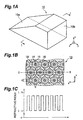
- Fig 1A is a perspective view of the optical component of the embodiment.
- An optical component 10 is formed by arraying a plurality of optical fibers parallel to each other. Each optical fiber is arrayed so that its fiber axis may be parallel to the y-axis in Fig. 1A, and the optical component 10 has an incident plane 10a being cut obliquely to the fiber axis, and an exit plane 10b being cut vertically to the fiber axis, in which the input pattern entering the incident plane 10a is reduced and is emitted from the exit plane10b.
- Fig. 1B is a magnified sectional view being cut by a plane parallel to the xz plane along the line I-I in Fig. 1A.
- the optical component 10 has a plurality of optical fibers comprising a first clad 14, a core 15 formed around the first clad 14, and a second clad 16 formed around the core 15, arrayed regularly so that the fiber axes may be parallel to each other. Between the optical fibers, a light absorbent 18 is provided for removing stray light in the optical component 10, and the second clad 16 of each optical fiber is integrally formed by heating and pressing, and fills up the gap between adjacent optical fibers.
- the section of the first clad 14 is nearly circular, and the section (outer circumference) of the core 15 is a nearly regular hexagon with crushed corners.
- materials of the first clad 14, core 15, and second clad 16 should be selected so that the viscosity of the first clad 14 and second clad 16 may be larger than the viscosity of the core 15.
- the diameter (a) of the first clad 14 is larger than the width (a') of the linear portion (or the portion close to the linear portion) of the section of the core 15, but in order to have a wider effective light receiving area (sectional area of core 15) on the incident plane 10a, the diameter (a) of the first clad 14 is preferred to be small.
- the width (b) of the second clad 16 for filling up the gap between cores is required to have a sufficient thickness to function as the clad, and in particular it is preferred to be more than 1/2 of the wavelength (550 nm) being used generally in the optical component 10.
- the diameter (a) of the first clad 14 is about 2 ⁇ m
- the width (a') of the flat portion of the section of the core 15 is about 4 ⁇ m
- the width (b) of the second clad 16 filling up the gap of cores is about 2 ⁇ m.
- the outside diameter of the core 15 is about 10 ⁇ m.
- the first clad 14 is made of, for example, borosilicate glass with refractive index n 1 of 1.495
- the core 15 is made of, for example, Ba-La glass with refractive index n 2 of 1.82
- the second clad 16 is made of, for example, borosilicate glass with refractive index n 3 of 1.495. Therefore, the refractive index distribution along line II-II in Fig. 1B is as shown in Fig. 1C.
- the refractive index n 2 of the core 15 is larger than the refractive index n 1 of the first clad 14, and the refractive index n 3 of the second clad 16 is smaller than the refractive index n 2 of the core 15.
- the refractive index n 1 of the first clad 14 and the refractive index n 3 of the second clad 16 are equal to each other. to each other.
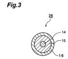
- FIG. 2A to Fig. 2E are manufacturing process charts of the optical fiber pair for composing the optical component 10
- Fig. 2F to Fig. 2H are sectional views of base materials and others manufactured in each process.
- a first clad base material 20 having a circular columnar shape is manufactured (Fig. 2A, Fig. 2F).
- the first clad base material 20 is made of, for example, borosilicate glass with refractive index of 1.495, and its side surface is polished by seria polishing or other method.
- the core base material 22 having a pipe shape manufactured separately as shown in Fig. 2B is filled up with the first clad base material 20 manufactured in the above process (Fig. 2C, Fig. 2G).
- the core base material 22 is made of, for example, Ba-La glass with refractive index of 1.82, and its inner surface and outer surface are polished by seria polishing or other method.
- the first clad base material 20 placed in the core base material 22 manufactured in the above process is inserted into a second clad base material 24 having a pipe shape as shown in Fig. 2D, and a base material 26 for manufacturing an optical fiber is manufactured (Fig. 2E, Fig. 2H).
- the second clad base material 24 is made of, for example, borosilicate glass with refractive index of 1.495, and one bottom 24a of the second clad base material 24 is sealed by burner or other melting method.
- the plurality of optical fibers 28 thus manufactured in the above process are disposed parallel to each other while properly disposing the light absorbent 18 in the gaps thereof, and formed integrally by heating and pressing, so that the optical component 10 is manufactured.
- Fig. 4 changes of the viscosity of the first clad 14, core 15 and second clad 16 in relation to the ambient temperature. As known from Fig. 4, at the temperature (about 850°c of heating and pressing process of the optical fiber, as compared with the viscosity of the core 15, the viscosity of the first clad 14 and second clad 16 is larger.
- optical component in this embodiment, problems of the optical component of the prior art are clarified.
- manufacture of optical component according to the prior art usually, a plurality of optical fibers with circular or square section are disposed and bundled parallel to each other, and formed integrally.
- the bundled optical fiber group is further drawn in wires (multi-fibers), and disposed parallel, bundle and formed integrally, or by repeating the drawing process and bundling process plural times (multi-multi-fibers), the optical component is formed integrally.
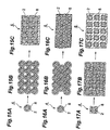
- Fig. 15A to Fig. 15C show changes in sectional shape of a core 2 when an optical component 6 is formed by disposing optical fibers 4 with the core 2 having a circular section at four corners.
- the optical component 6 is formed by disposing the optical fibers 4 with the core 2 having a circular section at four corners, as shown in Fig. 15A to Fig. 15c, by heating and pressing process when forming integrally by bundling the optical fibers 4, the section of the core 2 of each optical fiber 4 is deformed into a nearly square shape.
- the degree of deformation varies with the hardness of the core 2 and clad 8 of the optical fiber 4 under temperature in the heating and pressing process. If the core 2 is extremely hard as compared with the clad 8, the core 2 can be maintained in a circular section, but in order to avoid mutual contact of adjacent cores 2, it is practically difficult to increase the hardness of the core 2 extremely as compared with the clad 8.
- Fig. 16A to Fig. 16C show changes in the sectional shape of the core 2 when the optical component 6 is formed by disposing optical fibers 4 with the core 2 having a circular section at six corners. In this case, by heating and pressing process when forming integrally by bundling the optical fibers 4, the section of the core 2 of each optical fiber 4 is deformed into a nearly hexagonal shape.
- Fig. 17A to Fig. 17C show changes in the sectional shape of the core 2 when the optical component 6 is formed by disposing optical fibers 4 with the core 2 having a square section at four corners. In this case, since there is no gap between the adjacent clads 8 when disposing each optical fiber4, the section of the core 2 is maintained in square even after heating and pressing process when forming integrally by bundling the optical fibers 4.
- the section of the core 2 of each optical fiber 4 is a polygon having mutually parallel diagonals such as square and hexagon, the following problems are known. That is, the progress of the light entering the incident plane of the optical component 6 in the core 2 may take place in two modes, that is, spiral progress as shown in Fig. 18A to Fig. 18C, and band-like progress as shown in Fig. 19A to Fig. 19C. In Fig. 18A to Fig. 18C and Fig. 19A to Fig. 19C, the white circles and black circles show the light incident positions.
- Fig. 18A shows the mode of progress of the light entering the incident plane (core 2 incident plane) 6a of the optical component 6 within the core 2
- Fig. 18B is a projection of the light progress locus on a plane parallel to the incident plane 6a.
- the light entering the incident plane 7a of the optical component 6 at random incident angles (excluding the specified incident angle explained in Fig. 19A to Fig. 19C) progresses spirally in the core 2.
- Fig. 18C if the light enters the incident plane 6a of the optical component 6 at a specific incident angle ⁇ , it is emitted at various exit angles from the exit plane 6b of the optical component 6 due to difference in the incident position.
- the light entering the incident plane 6a of the optical component 6 at a specified incident angle progresses in the core 2 in a band pattern.
- the light entering the incident plane 6a of the optical component 6 at specific incident angle ⁇ is emitted from the exit 6b of the optical component 6 also at the same exit angle ⁇ regardless of difference in the incident position. Therefore, in the output image emitted from the exit plane 6b of the optical component 6, a pattern having an intensity only in a specific exit angle is formed, and this pattern becomes noise to lower the resolution of the optical component 6.
- multi-multi-fibers since the optical component manufactured by integrally forming multi-fibers (multi-multi-fibers) differs in the degree of deformation of the core 2 between the central part and edge part of the multi-fibers, pattern noise depending on the sectional shape of the multi-fibers is caused due to difference in the degree of deformation, and the resolution of the optical component 6 is extremely lowered.
- the optical component 10 of the embodiment is as follows.
- each optical fiber comprises the first clad 14, core 15 formed around the first clad 14, and second clad 16 formed around the core 15, the light entering the incident plane 10a is reflected repeatedly on the interface of the first clad 14 and core 15 and the interface of the second clad 16 and core 15, and propagates in the core 15.
- Fig. 10 For example, as shown in Fig.
- the critical angle at the interface of the core 15 and first clad 14 and the critical angle at the interface of the core 15 and second clad 16 are equal to each other.
- the optical component 10 by forming the optical fibers for composing the optical component 10 by the first clad 1 with a nearly circular section, core 15 formed around the first clad 14, and second clad 16 formed around the core 15, any pattern having an intensity only in a specific exit angle is not formed. As a result, pattern noise can be prevented, and an output image of a high resolution can be obtained from the exit plane 10b of the optical component 10.
- the critical angle at the interface of the core 15 and first clad 14 and the critical angle at the interface of the core 15 and second clad 16 are equal to each other, the light of total reflection on the interface of the core 15 and first clad 14 is always reflected totally on the interface of the core 15 and second clad 16, and also the light of total reflection on the interface of the core 15 and second clad 16 is always reflected totally on the interface of the core 15 and first clad 14, so that light transmission of high efficiency is realized.
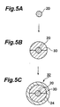
- base materials 26 are formed in the method shown in Fig. 2F to Fig. 2H, the following method may be also applicable. That is, as shown in Fig. 5A to Fig. 5C, first, a first clad base material (Fig. 5A) having a circular columnar shape is manufactured, and two core base materials 30 having a shape of dividing a thick-wall cylinder into two sections at a plane vertical to the bottom are disposed around it (Fig. 5B). The first clad base material 20 surrounded with the core base materials 30 manufactured in this process is charged into a second clad base material 24 of pipe shape, and a base material 32 for manufacturing optical fiber is manufactured (Fig. 5C). One bottom 24a of the second clad base material 24 is sealed by burner or other melting method. The subsequent process, that is, formation of the optical fiber 28 by drawing the base material 32 in wire and formation of optical component 10 are same as mentioned above.
- the base materials for forming the optical fibers 28 for composing the optical component 10 may be also manufactured in the following method. That is, as shown in Fig. 6A to Fig. 6C, a first clad base material 20 having a circular columnar shape is manufactured (Fig. 6A), and a plurality of core base materials 34 having a circular columnar shape are disposed around it (Fig. 6B). The first clad base material 20 surrounded with the core base materials 34 manufactured in the above process is put in a second clad base material 24 having a pipe shape, and a base material 36 for manufacturing optical fibers is made (Fig. 6C). One bottom 24a of the second clad base material 24 is sealed by burner or other melting method. The subsequent process, that is, formation of the optical fiber 28 by drawing the base material 36 in wire and formation of optical component 10 are same as mentioned above.
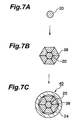
- the base materials for forming the optical fibers 28 for composing the optical component10 may be also manufactured in the following method. That is, as shown in Fig. 7A to Fig. 7C, a first clad base material 20 having a circular columnar shape is manufactured (Fig. 7A), and a plurality of core base materials 38 having a square columnar shape are disposed around it (Fig. 7B). The first clad base material 20 surrounded with the core base materials 38 manufactured in the above process is put in a second clad base material 24 having a pipe shape, and a base material 40 for manufacturing optical fibers is made (Fig. 7C). One bottom 24a of the second clad base material 24 is sealed by burner or other melting method. The subsequent process, that is, formation of the optical fiber 28 by drawing the base material 40 in wire and formation of optical component 10 are same as mentioned above.
- each optical fiber for composing the optical component 10 comprises a first clad 14 of a nearly circular section, a core 15 disposed around the first clad 14, and a second clad 16 disposed around the core 15.
- Fig. 8 is a magnified sectional view of an optical component 50 in a first modified example.
- the optical component 50 differs from the optical component 10 in the first embodiment is that the optical component 50 does not have light absorbent 18.
- the diameter (a) of the first clad 14 is larger than the width (a') of the linear portion (or the portion close to the linear portion) of the section of the core 15, it is possible to eliminate completely the band-like progress of the light mentioned in the prior art. It is required that the width (b) of the second clad 16 for filling up the gap of each core should have a sufficient thickness to function as the clad.
- Fig. 9 is a magnified sectional view of an optical component 60 in a second modified example.
- the optical component 60 differs from the optical component 50 of the first modified example is that the optical component 60 has a flat shape in the interface (outer circumference) of the core 15 whereas the optical component 50 has a curved shape in the interface (outer circumference) of the core 15.
- the optical component 60 having such sectional shape can be obtained by selecting the materials for the first clad 14, core 15 and second clad 16 so that the viscosity of the core 15 may be extremely small as compared with the viscosity of the first clad 14 and second clad 16 in the heating and pressing process of the optical fiber.
- the diameter (a) of the first clad 14 is larger than the width (a') of the linear portion of the section of the core 15, but in order to increase the effective light receiving area (sectional area of the core 15) at the incident plane 10a, the diameter (a) of the first clad 14 is preferred to be smaller, and hence the diameter of the first clad 14 should be properly selected in consideration of the resolution, effective light receiving area, etc. It is also required that the width (b) of the second clad 16 for filling up the gap of each core should have a sufficient thickness to function as the clad.
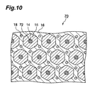
- Fig. 10 is a magnified sectional view of an optical component 70 in a third modified example.
- the optical component 70 differs from the optical component 10 in the first embodiment is that the optical component 70 has a light absorbent 72 provided in the first clad 14. By putting the light absorbent 72 in the first clad 14, the light advancing into the first clad 14 can be effectively removed by the light absorbent 72.
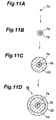
- Fig. 11A to Fig. 11D are manufacturing process charts of the optical component 70 in the third modified example.
- a circular columnar base material 74 for light absorbent is manufactured (Fig. 11A), and its surrounding is covered with a first clad base material 76, and a circular columnar first clad base material 76 is formed (Fig. 11B).
- Fig. 11C a circular columnar first clad base material 22
- Fig. 11D are same as mentioned above.
- manufactured base material 78 is drawn in wires, and formed integrally, and the optical component 70 is obtained.
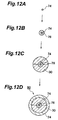
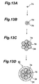
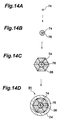
- the optical component 70 of the third modified example may be also manufactured in the methods as shown in Fig. 12A to Fig. 12D, Fig. 13A to Fig. 13D, and Fig. 14A to Fig. 14D. That is, in the process of disposing the core base material around the first clad base material 76, two core base materials 30 having a shape of dividing a thick-wall cylinder into two sections at a plane vertical to the bottom may be disposed (Fig. 12C), a plurality of core base materials 34 having a circular columnar shape may be disposed (Fig. 13C), or a plurality of core base materials 38 having a square columnar shape may be disposed (Fig. 14C).
- optical components 10, 50, 60, and 70 in the foregoing embodiments are optical parts formed by arraying a plurality of optical fibers parallel to each other, but the optical components may be formed in a taper shape for emitting the light entering the incident plane in a magnified or reduced image, by arraying a plurality of optical fibers in a curved form.
- This optical component has numerous benefits including a high transmission efficiency and a smaller in size of optical system as compared with the lens, and is hence used in various fields such as fingerprint detecting system and radiation detector.
Landscapes
- Engineering & Computer Science (AREA)
- Chemical & Material Sciences (AREA)
- Physics & Mathematics (AREA)
- Life Sciences & Earth Sciences (AREA)
- General Life Sciences & Earth Sciences (AREA)
- Geochemistry & Mineralogy (AREA)
- Manufacturing & Machinery (AREA)
- Materials Engineering (AREA)
- Organic Chemistry (AREA)
- General Physics & Mathematics (AREA)
- Optics & Photonics (AREA)
- Optical Fibers, Optical Fiber Cores, And Optical Fiber Bundles (AREA)
Applications Claiming Priority (3)
| Application Number | Priority Date | Filing Date | Title |
|---|---|---|---|
| JP8880598 | 1998-04-01 | ||
| JP8880598 | 1998-04-01 | ||
| PCT/JP1999/001485 WO1999050695A1 (fr) | 1998-04-01 | 1999-03-24 | Piece optique |
Publications (3)
| Publication Number | Publication Date |
|---|---|
| EP1069446A1 true EP1069446A1 (de) | 2001-01-17 |
| EP1069446A4 EP1069446A4 (de) | 2002-11-27 |
| EP1069446B1 EP1069446B1 (de) | 2005-03-16 |
Family
ID=13953109
Family Applications (1)
| Application Number | Title | Priority Date | Filing Date |
|---|---|---|---|
| EP99910680A Expired - Lifetime EP1069446B1 (de) | 1998-04-01 | 1999-03-24 | Optisches faserbündel zur übertragung von bildern |
Country Status (6)
| Country | Link |
|---|---|
| US (1) | US6567593B1 (de) |
| EP (1) | EP1069446B1 (de) |
| CN (1) | CN1138159C (de) |
| AU (1) | AU2957399A (de) |
| DE (1) | DE69924243T2 (de) |
| WO (1) | WO1999050695A1 (de) |
Cited By (1)
| Publication number | Priority date | Publication date | Assignee | Title |
|---|---|---|---|---|
| US11377384B2 (en) | 2017-01-19 | 2022-07-05 | University Of Bath | Method of making an imaging fibre apparatus and optical fibre apparatus with different core |
Families Citing this family (7)
| Publication number | Priority date | Publication date | Assignee | Title |
|---|---|---|---|---|
| JP4202567B2 (ja) * | 1999-11-30 | 2008-12-24 | 浜松ホトニクス株式会社 | 光学部品の製造方法 |
| CN102236133B (zh) * | 2010-04-29 | 2013-09-25 | 光燿科技股份有限公司 | 光纤连接头及其制造方法 |
| US9027540B2 (en) | 2011-01-28 | 2015-05-12 | Copper John Corporation | Bowstring release |
| USD688346S1 (en) * | 2011-08-12 | 2013-08-20 | Scott Archery Manufacturing | Archery release |
| CN103969734B (zh) * | 2013-02-05 | 2017-09-05 | 鸿富锦精密工业(深圳)有限公司 | 图像补偿装置、显示装置及拼接型显示装置 |
| US10145646B2 (en) | 2014-11-13 | 2018-12-04 | Scott Archery Llc | Archery bowstring release enabling sensitivity adjustment |
| CN117285246A (zh) * | 2023-09-05 | 2023-12-26 | 武汉睿芯特种光纤有限责任公司 | 具有多边形纤芯的光纤及其制备方法 |
Family Cites Families (18)
| Publication number | Priority date | Publication date | Assignee | Title |
|---|---|---|---|---|
| US3275428A (en) * | 1963-05-21 | 1966-09-27 | American Optical Corp | Method of making honeycomb structure |
| US3715150A (en) * | 1971-09-14 | 1973-02-06 | Corning Glass Works | Photochromic fiber optic plate |
| US4000416A (en) * | 1975-07-11 | 1976-12-28 | International Telephone And Telegraph Corporation | Multi-core optical communications fiber |
| US4237550A (en) * | 1979-06-08 | 1980-12-02 | International Telephone And Telegraph Corporation | Multiuser protected optical data bus distribution systems |
| US4759604A (en) * | 1985-12-20 | 1988-07-26 | Mitsubishi Cable Industries Ltd. | Optical multiconductor of silica glass type |
| US4806289A (en) * | 1987-01-16 | 1989-02-21 | The Dow Chemical Company | Method of making a hollow light pipe |
| JP2886599B2 (ja) * | 1990-02-27 | 1999-04-26 | 株式会社フジクラ | イメージファイバの製造方法 |
| JPH0459608A (ja) | 1990-06-27 | 1992-02-26 | Shin Etsu Chem Co Ltd | 窒化アルミニウムの連続的製造方法 |
| US5111525A (en) | 1990-10-15 | 1992-05-05 | General Dynamics Corporation | Split-core fiber optic waveguide and sensor |
| JPH06174948A (ja) * | 1992-12-04 | 1994-06-24 | Fujikura Ltd | イメージファイバ |
| JPH07113920A (ja) * | 1993-10-19 | 1995-05-02 | Olympus Optical Co Ltd | イメージファイバー |
| JPH08338916A (ja) * | 1995-06-12 | 1996-12-24 | Hamamatsu Photonics Kk | ファイバー光学プレート |
| US5940565A (en) * | 1996-07-24 | 1999-08-17 | Hamamatsu Photonics K.K. | Fiber optic device, light receiving member, and pattern acquisition apparatus |
| JPH10153711A (ja) * | 1996-09-30 | 1998-06-09 | Bridgestone Corp | 分岐型光伝送装置 |
| US6174604B1 (en) * | 1997-02-28 | 2001-01-16 | The Furukawa Electric Co., Ltd. | Optical-fiber core binder and optical fiber unit |
| JP3621220B2 (ja) * | 1997-03-17 | 2005-02-16 | 富士通株式会社 | 光増幅器及び光導波構造 |
| JP3248103B2 (ja) | 1998-12-04 | 2002-01-21 | 日本プレシジョン・サーキッツ株式会社 | Mosトランジスタ出力回路 |
| JP4059608B2 (ja) * | 2000-03-09 | 2008-03-12 | 新日本製鐵株式会社 | 焼結鉱の還元粉化試験自動装置 |
-
1999
- 1999-03-24 EP EP99910680A patent/EP1069446B1/de not_active Expired - Lifetime
- 1999-03-24 AU AU29573/99A patent/AU2957399A/en not_active Abandoned
- 1999-03-24 WO PCT/JP1999/001485 patent/WO1999050695A1/ja not_active Ceased
- 1999-03-24 CN CNB998053910A patent/CN1138159C/zh not_active Expired - Fee Related
- 1999-03-24 DE DE69924243T patent/DE69924243T2/de not_active Expired - Fee Related
-
2000
- 2000-09-29 US US09/672,788 patent/US6567593B1/en not_active Expired - Fee Related
Cited By (2)
| Publication number | Priority date | Publication date | Assignee | Title |
|---|---|---|---|---|
| US11377384B2 (en) | 2017-01-19 | 2022-07-05 | University Of Bath | Method of making an imaging fibre apparatus and optical fibre apparatus with different core |
| US11577986B2 (en) | 2017-01-19 | 2023-02-14 | University Of Bath | Method of making an imaging fibre apparatus and optial fibre apparatus with different core |
Also Published As
| Publication number | Publication date |
|---|---|
| DE69924243D1 (de) | 2005-04-21 |
| EP1069446B1 (de) | 2005-03-16 |
| EP1069446A4 (de) | 2002-11-27 |
| US6567593B1 (en) | 2003-05-20 |
| CN1298491A (zh) | 2001-06-06 |
| WO1999050695A1 (fr) | 1999-10-07 |
| AU2957399A (en) | 1999-10-18 |
| CN1138159C (zh) | 2004-02-11 |
| DE69924243T2 (de) | 2006-02-09 |
Similar Documents
| Publication | Publication Date | Title |
|---|---|---|
| US5631994A (en) | Structured surface light extraction overlay and illumination system | |
| EP0803746B1 (de) | Verbindung von optischen Faserbündeln | |
| US9864150B2 (en) | Optical interconnection component | |
| EP1076247B1 (de) | Optische Faserbündel zur Übertragung von Bildern | |
| EP1069446A1 (de) | Optisches teil | |
| EP0821248B1 (de) | Faseroptisches Element, lichtempfangendes Element, und Vorrichtung zur Mustererfassung | |
| EP1001283B1 (de) | Optisches element,abbildeeinheit,abbildevorrichtung,strahlungsabbildungssensor und fingerabdruckanalysator unter verwendung derselben | |
| JP6778633B2 (ja) | コンバイナ、光デバイス、及び製造方法 | |
| JPWO1999056162A1 (ja) | 光学部品 | |
| EP1069445A1 (de) | Optisches element | |
| EP1076246B1 (de) | Optisches faserbündel zur bildübertragung und sein herstellungsverfahren | |
| EP1061385B1 (de) | Faseroptische Komponente zur Bildübertragung | |
| EP1001285A1 (de) | Optisches element und eine dieses verwendende abbildungsvorrichtung | |
| JP4202567B2 (ja) | 光学部品の製造方法 | |
| JPWO1999040464A1 (ja) | 光学部品 | |
| WO2004068204A1 (en) | Method and apparatus for coupling light | |
| EP1211530A2 (de) | Optische Kopplungsvorrichtung mit anisotropem lichtleitendem Element | |
| JPWO1999056161A1 (ja) | 光学部品及びその製造方法 | |
| JPWO1999050695A1 (ja) | 光学部品 | |
| WO2025021671A1 (en) | Flexible optical waveguides | |
| Kociszewski et al. | Technological aspects of fiber optic integrated structures manufacturing | |
| JPWO1999050694A1 (ja) | 光学部品 | |
| JPH09230147A (ja) | ファイバー光学プレート | |
| MXPA98001304A (en) | Overclock for extraction of light with a structured surface and lighting system |
Legal Events
| Date | Code | Title | Description |
|---|---|---|---|
| PUAI | Public reference made under article 153(3) epc to a published international application that has entered the european phase |
Free format text: ORIGINAL CODE: 0009012 |
|
| 17P | Request for examination filed |
Effective date: 20001030 |
|
| AK | Designated contracting states |
Kind code of ref document: A1 Designated state(s): BE DE FR GB IT |
|
| A4 | Supplementary search report drawn up and despatched |
Effective date: 20021015 |
|
| AK | Designated contracting states |
Kind code of ref document: A4 Designated state(s): BE DE FR GB IT |
|
| 17Q | First examination report despatched |
Effective date: 20031202 |
|
| GRAP | Despatch of communication of intention to grant a patent |
Free format text: ORIGINAL CODE: EPIDOSNIGR1 |
|
| RTI1 | Title (correction) |
Free format text: OPTICAL FIBRE BUNDLE FOR IMAGE TRANSMISSION |
|
| GRAS | Grant fee paid |
Free format text: ORIGINAL CODE: EPIDOSNIGR3 |
|
| GRAA | (expected) grant |
Free format text: ORIGINAL CODE: 0009210 |
|
| AK | Designated contracting states |
Kind code of ref document: B1 Designated state(s): BE DE FR GB IT |
|
| REG | Reference to a national code |
Ref country code: GB Ref legal event code: FG4D |
|
| REF | Corresponds to: |
Ref document number: 69924243 Country of ref document: DE Date of ref document: 20050421 Kind code of ref document: P |
|
| ET | Fr: translation filed | ||
| PLBE | No opposition filed within time limit |
Free format text: ORIGINAL CODE: 0009261 |
|
| STAA | Information on the status of an ep patent application or granted ep patent |
Free format text: STATUS: NO OPPOSITION FILED WITHIN TIME LIMIT |
|
| 26N | No opposition filed |
Effective date: 20051219 |
|
| PGFP | Annual fee paid to national office [announced via postgrant information from national office to epo] |
Ref country code: IT Payment date: 20080327 Year of fee payment: 10 Ref country code: GB Payment date: 20080326 Year of fee payment: 10 |
|
| PGFP | Annual fee paid to national office [announced via postgrant information from national office to epo] |
Ref country code: FR Payment date: 20080311 Year of fee payment: 10 Ref country code: DE Payment date: 20080407 Year of fee payment: 10 |
|
| PGFP | Annual fee paid to national office [announced via postgrant information from national office to epo] |
Ref country code: BE Payment date: 20080522 Year of fee payment: 10 |
|
| BERE | Be: lapsed |
Owner name: *HAMAMATSU PHOTONICS K.K. Effective date: 20090331 |
|
| GBPC | Gb: european patent ceased through non-payment of renewal fee |
Effective date: 20090324 |
|
| REG | Reference to a national code |
Ref country code: FR Ref legal event code: ST Effective date: 20091130 |
|
| PG25 | Lapsed in a contracting state [announced via postgrant information from national office to epo] |
Ref country code: DE Free format text: LAPSE BECAUSE OF NON-PAYMENT OF DUE FEES Effective date: 20091001 |
|
| PG25 | Lapsed in a contracting state [announced via postgrant information from national office to epo] |
Ref country code: BE Free format text: LAPSE BECAUSE OF NON-PAYMENT OF DUE FEES Effective date: 20090331 |
|
| PG25 | Lapsed in a contracting state [announced via postgrant information from national office to epo] |
Ref country code: GB Free format text: LAPSE BECAUSE OF NON-PAYMENT OF DUE FEES Effective date: 20090324 Ref country code: FR Free format text: LAPSE BECAUSE OF NON-PAYMENT OF DUE FEES Effective date: 20091123 |
|
| PG25 | Lapsed in a contracting state [announced via postgrant information from national office to epo] |
Ref country code: IT Free format text: LAPSE BECAUSE OF NON-PAYMENT OF DUE FEES Effective date: 20090324 |