EP1067671B1 - Power supply circuit of an electric motor and corresponding control method - Google Patents
Power supply circuit of an electric motor and corresponding control method Download PDFInfo
- Publication number
- EP1067671B1 EP1067671B1 EP99830423A EP99830423A EP1067671B1 EP 1067671 B1 EP1067671 B1 EP 1067671B1 EP 99830423 A EP99830423 A EP 99830423A EP 99830423 A EP99830423 A EP 99830423A EP 1067671 B1 EP1067671 B1 EP 1067671B1
- Authority
- EP
- European Patent Office
- Prior art keywords
- voltage
- signal
- phase
- generating
- mains
- Prior art date
- Legal status (The legal status is an assumption and is not a legal conclusion. Google has not performed a legal analysis and makes no representation as to the accuracy of the status listed.)
- Expired - Lifetime
Links
Images


Classifications
-
- H—ELECTRICITY
- H02—GENERATION; CONVERSION OR DISTRIBUTION OF ELECTRIC POWER
- H02P—CONTROL OR REGULATION OF ELECTRIC MOTORS, ELECTRIC GENERATORS OR DYNAMO-ELECTRIC CONVERTERS; CONTROLLING TRANSFORMERS, REACTORS OR CHOKE COILS
- H02P25/00—Arrangements or methods for the control of AC motors characterised by the kind of AC motor or by structural details
- H02P25/02—Arrangements or methods for the control of AC motors characterised by the kind of AC motor or by structural details characterised by the kind of motor
- H02P25/04—Single phase motors, e.g. capacitor motors
Definitions
- the present invention relates to a power supply circuit of the stabilized, or at least regulated, voltage type, for an electric motor, for the purpose of maximizing the efficiency of the motor or of regulating its speed, particularly for an asynchronous electric motor, and especially - but not exclusively - a single-phase asynchronous motor.
- the present invention also relates to an electric motor comprising a power supply circuit of the stabilized voltage type, as well as a method for controlling the supply voltage of an electric motor.
- the power supply is at a constant voltage
- the motor is designed with the object of optimizing the performance of the motor at the design voltage, typically ranging from 200 to 230 V, or having other values according to the mains voltage used in the country in which the motor is to be used.
- the supply voltage is not constant, as a result of possible voltage fluctuations in the mains, and also as a result of small differences in voltage in the various mains systems of the individual countries in which the motor may be used.
- the mains voltage may be as much as 255 V.
- control circuits based on the principle of slicing, particularly triac and chopper control circuits, are used at present. These circuits have some disadvantages, including a high harmonic content of the supply voltage to the motor (particularly for triac controllers) and a high cost, owing to the necessity of using high-voltage components and complicated control circuits.
- the production of chopper control circuits also has the disadvantage of a certain structural complexity due to the necessity of using controlled switches which operate at a high frequency with respect to the mains frequency.
- US-A-4347474 discloses a method for supplying an electric motor with a controlled voltage and a circuit for controlling the power supply voltage of an electric motor.
- This known circuit comprises means for measuring the difference between a mains voltage and a reference voltage and means for generating an alternating correction reference whose frequency is equal to the frequency of the mains voltage and which is phase-shifted with respect to said mains voltage.
- US-A_5283726 discloses an AC line current controller for use in combination with an electric motor.
- the object of the present invention is to provide a new type of control circuit for the power supply of a motor, particularly an asynchronous motor, which can be used to set or stabilize the supply voltage while avoiding the disadvantages of traditional slicing circuits.
- a further object of the present invention is to provide a new method of controlling the power supply to an electric motor, particularly an asynchronous motor, which enables a stabilized supply voltage to be obtained without the disadvantages of the conventional methods.
- the object of the present invention is to provide a circuit and a control method which do not require expensive components, which avoid the use of high-frequency switching elements, and which do not require mains filters for the elimination of electromagnetic noise.
- circuit characterized in that it comprises means of measuring a difference between a mains voltage and a reference voltage, and means for generating an alternating correction voltage whose frequency is equal to the frequency of the mains voltage, and which is phase-shifted with respect to said mains voltage, the phase shift between the mains voltage and the correction voltage being proportional to the difference between the mains voltage and the reference voltage, and said correction voltage being added to the mains voltage.
- the invention is based on the idea of subtracting from, or adding to, the mains voltage an alternating wave at low voltage (correction voltage), whose phase with respect to the mains voltage is controlled in such a way that the sum of the two voltages supplies a stabilized voltage to the motor.
- the correction voltage it is possible to generate the correction voltage by using a full bridge consisting of four controlled switches, whose switching generates the correction voltage, which in this case is a square-wave voltage.
- a control logic switches the controlled switches according to the difference between the mains voltage and the value of the stabilized voltage which is required for the motor.
- the bridge of controlled switches is connected, through a direct-current branch of the bridge, to a virtually continuous voltage source.
- this virtually continuous voltage source may be a source supplied from the same mains voltage which has been suitably processed, in a particularly advantageous embodiment the continuous voltage is obtained by using the inductive energy of the motor.
- a storage device in which the inductive energy is stored during certain phases of the operating cycle, and transferred to the motor in the remaining phases, can be located in the direct-current branch of the bridge of controlled switches.
- the storage device consists of a capacitor or a group of capacitors.
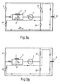
- Fig. 1 shows schematically a constant-voltage power supply circuit for a single-phase asynchronous motor.
- the number 1 indicates the alternating voltage source, consisting, for example, of the electrical power mains, a generator unit, or another source.
- the number 3 indicates in a general way the motor which is represented schematically as an inductor 5 in parallel with a resistor 7.
- the motor 3 and the voltage source 1 are connected in a full bridge consisting of controlled switches 11, 12, 13, 14, consisting for example of the same number of MOSFETs or other switching devices controlled by a control logic 17 whose outputs 17A-17D open and close the switches 11-14.
- a direct-current branch 18 comprising a storage capacitor 19 is connected in parallel with the bridge 11-14.
- the switching of the switches 11-14 is controlled by the control logic 17 according to the voltage across the terminals of the motor 3 and the phase of the supply voltage, in such a way as to generate a square-wave voltage which has a frequency equal to the frequency of the supply voltage supplied by the source 1, but is phase-shifted with respect to the latter, and which is added to or subtracted from the supply voltage to produce a voltage equal to the desired voltage across the terminals of the stator winding of the motor 3.
- the control logic modifies the phase of the square wave with respect to the phase of the supply voltage supplied by the source 1, to produce a voltage equal to the desired voltage across the terminals of the motor.
- the necessary voltage for the supply of the bridge 11-14 for generating the square wave is obtained by storing in the capacitor 19 some of the inductive energy of the motor 3.
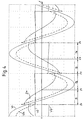
- Fig. 4 shows the following curves superimposed on each other
- the voltage V2 applied to the motor by the bridge 11-14 is a square-wave voltage with a frequency equal to the frequency of the supply voltage V1, but phase-shifted with respect to it.
- the voltage Vm across the motor is the algebraic sum of the two voltages V1 and V2.
- the phase shift between the voltages V1 and V2 is obtained by operating the controlled switches 11-14 of the full bridge and is controlled in such a way that it always supplies the motor 3 at a design voltage, independently of the voltage of the source 1.
- the mains voltage V1 is greater than the motor supply voltage Vm.
- the control circuit In practice, it is advantageous to make the control circuit impart a phase to the voltage V2 such that there is always a subtraction from the mains voltage V1, although, as will be clear to a person skilled in the art, the circuit can also operate in the opposite way.
- the motor is designed for a rated voltage value Vm which is lower than the minimum value which can be supplied by the mains. For example, for a motor suitable for operation in a voltage range of 210-240 V, the design voltage of the motor will be equal to or less than 210 V.
- control logic 17 will modify the switching phase of the switches 11,12,13 and 14 in such a way as to phase-shift the square-wave voltage V2 in a different way with respect to the mains voltage V1 to keep the sum Vm of the two voltages equal to the design value of the motor.
- FIG. 4 shows four time intervals T1, T2, T3 and T4 which correspond to the four states assumed in sequence by the control circuit in Fig. 1, according to the direction of flow of the current supplied by the voltage source 1 and the states of opening and closing of the switches 11, 12, 13, 14 of the full bridge.
- Figs. 3A-3D show the switching conditions of the switches and the direction of flow of the current in the circuit for each of the four intervals T1-T4.
- Fig. 3A shows the power supply circuit of the motor 3 during the interval T1 which starts at the instant (t0) at which the switches 11-14 of the bridge are switched and the voltage V1 is positive. Switches 11, 13 are open (OFF state), while switches 12 and 14 are closed (ON state).
- the polarity of the capacitor 19 matches the. polarity of the voltage source 1, so that the voltage V2 across the terminals of the capacitor 19 is added to the mains voltage V1.
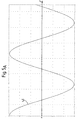
- the capacitor 19 discharges, supplying current to the motor 3. This is reflected in a slight decrease of the voltage Vc across the terminals of the capacitor in the interval T1 (see also Fig. 5E). However, the capacitance of the capacitor 19 is such that this voltage variation is minimized.
- the current Im in the motor has a sinusoidal variation which is phase-shifted with respect to the variation of the mains voltage V1 and, at the end of the interval T1 (at the instant t1), it passes through the zero value, changing the direction of flow.
- the circuit assumes. the configuration in Fig. 3B, which is maintained for the time interval T2 (t2-t1): the current Im flows through the capacitor 19 in a direction such that it is charged, as may be seen from the slightly increasing trend of the voltage Vc (see also Fig. 5E) in the interval T2 and energy, in the form of the reactive energy of the motor 3, is stored in the capacitor 19.
- switches 11, 12, 13 and 14 of the bridge are switched: switches 11, 13 are closed (ON state) and switches 12, 14 are opened (OFF state), while the current Im in the motor continues to flow in the same direction.
- the circuit assumes the configuration in Fig. 3C.
- the voltage applied by the bridge changes sign and becomes negative.
- the current in the capacitor 19 now flows in such a direction that energy is transferred from the capacitor to the motor, discharging the capacitor (the curve Vc is descending slightly).
- the instants of switching of the bridge 11, 12, 13, 14, which determine the phase of the square wave V2 with respect to the mains voltage V1 are delayed in such a way that the voltage V2 which is added algebraically to the voltage V1 maintains a voltage across the terminals of the stator winding of the motor 3 which is less than the mains voltage.
- This is on the assumption that the motor has been designed for a rated voltage lower than the mains voltage, for example on the assumption that the design voltage is 210 V and the mains voltage is 230 V.
- the control logic 17 modifies the phase of the square-wave voltage V2 in such a way that the design voltage of 210 V is still produced across the terminals of the stator winding of the motor. Similar behaviour can take place if the design voltage is greater than the mains voltage, in which case the phase of the square wave V2 will be selected in such a way as to increase the voltage across the terminals of the motor with respect to the mains voltage.
- the full bridge 11, 12, 13, 14 is caused to switch by finding the phase of the mains voltage V1 and the value of the voltage across the terminals of the motor 3, and then switching the switches 11, 12, 13,14 in such a way as to obtain the desired phase for the square wave V2 so that the voltage to the motor remains at the desired value.
- the control logic 17 which causes the switching of the bridge 11, 12, 13, 14 may have the configuration shown in Fig. 2.
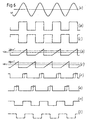
- the waveforms of the various signals in the control logic 17 are reproduced in Figs. 6A-6I.
- a periodic signal (see Fig. 6B) in phase with the mains voltage V1, which is sent to the input of a first ramp generator 23.
- the signal at the output of the detector 21 is also sent to an inverter 25, at whose output is obtained a signal which is inverted with respect to the output signal of the detector 21 (Fig. 6C), and which is sent to the input of a second ramp generator 27.
- 6D and 6E are obtained at the outputs of the two ramp generators.
- the two signals at the outputs of the ramp generators 23, 27 are sent to a first input of two corresponding comparators 29, 31, to whose second input is applied an error voltage (Verr) proportional to the difference between the design voltage of the motor (Vp) and the mains voltage (V1).
- Verr error voltage
- the output signal of the comparator 29 is shown in Fig. 6F in solid lines.
- Figs. 6D to 6I also show how the phase of the switching signal generated by the flip-flop 33 varies with a variation of the error voltage.
- Figs. 6D and 6E show in broken lines a different value of the error voltage V'err, which causes the generation of output signals of the comparators 29, 31 indicated in broken lines in Figs. 6F and 6G. These two signals, applied to the set and reset inputs of the flip-flop 33, generate the switching signal indicated in Fig. 6I.
- This last signal has the same frequency as the signal in Fig. 6H, but is phase-shifted with respect to it.
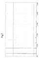
- Fig. 7 shows the spectrum of the harmonic content of the voltage applied to the motor. As shown in the diagram, the harmonics of the base signal at 50 Hz are negligible, with considerable advantages over the situation which occurs when the voltage is controlled by triac slicers.
Landscapes
- Engineering & Computer Science (AREA)
- Power Engineering (AREA)
- Control Of Ac Motors In General (AREA)
- Control Of Electric Motors In General (AREA)
- Control Of Motors That Do Not Use Commutators (AREA)
- Control Of Direct Current Motors (AREA)
Priority Applications (12)
| Application Number | Priority Date | Filing Date | Title |
|---|---|---|---|
| DE69905453T DE69905453T2 (de) | 1999-07-02 | 1999-07-02 | Stromversorgungseinrichtung für einen elektrischen Motor und dazugehörige Steuerungsmethode |
| EP99830423A EP1067671B1 (en) | 1999-07-02 | 1999-07-02 | Power supply circuit of an electric motor and corresponding control method |
| DK99830423T DK1067671T3 (da) | 1999-07-02 | 1999-07-02 | Strømforsyningskredsløb til en elektrisk motor og tilhørende styrefremgangsmåde |
| ES99830423T ES2191408T3 (es) | 1999-07-02 | 1999-07-02 | Circuito de alimentacion de corriente de un motor electrico y el correspondiente metodo de control. |
| AT99830423T ATE233025T1 (de) | 1999-07-02 | 1999-07-02 | Stromversorgungseinrichtung für einen elektrischen motor und dazugehörige steuerungsmethode |
| US10/030,025 US6775161B1 (en) | 1999-07-02 | 2000-06-26 | Power supply circuit for an electric motor and corresponding control method |
| PCT/IT2000/000261 WO2001003283A1 (en) | 1999-07-02 | 2000-06-26 | Power supply circuit of an electric motor and corresponding control method |
| JP2001508582A JP2003504998A (ja) | 1999-07-02 | 2000-06-26 | 電動モーターの電力供給回路及びそれに対応する制御方法 |
| BR0012456-7A BR0012456A (pt) | 1999-07-02 | 2000-06-26 | Circuito de suprimento de energia de um motor elétrico e método de controle correspondente |
| CA002377980A CA2377980C (en) | 1999-07-02 | 2000-06-26 | Power supply circuit of an electric motor and corresponding control method |
| AU58451/00A AU5845100A (en) | 1999-07-02 | 2000-06-26 | Power supply circuit of an electric motor and corresponding control method |
| CNB008098891A CN100530936C (zh) | 1999-07-02 | 2000-06-26 | 控制电机的电源电路、电机、以及相应的控制方法 |
Applications Claiming Priority (1)
| Application Number | Priority Date | Filing Date | Title |
|---|---|---|---|
| EP99830423A EP1067671B1 (en) | 1999-07-02 | 1999-07-02 | Power supply circuit of an electric motor and corresponding control method |
Publications (2)
| Publication Number | Publication Date |
|---|---|
| EP1067671A1 EP1067671A1 (en) | 2001-01-10 |
| EP1067671B1 true EP1067671B1 (en) | 2003-02-19 |
Family
ID=8243490
Family Applications (1)
| Application Number | Title | Priority Date | Filing Date |
|---|---|---|---|
| EP99830423A Expired - Lifetime EP1067671B1 (en) | 1999-07-02 | 1999-07-02 | Power supply circuit of an electric motor and corresponding control method |
Country Status (12)
| Country | Link |
|---|---|
| US (1) | US6775161B1 (zh) |
| EP (1) | EP1067671B1 (zh) |
| JP (1) | JP2003504998A (zh) |
| CN (1) | CN100530936C (zh) |
| AT (1) | ATE233025T1 (zh) |
| AU (1) | AU5845100A (zh) |
| BR (1) | BR0012456A (zh) |
| CA (1) | CA2377980C (zh) |
| DE (1) | DE69905453T2 (zh) |
| DK (1) | DK1067671T3 (zh) |
| ES (1) | ES2191408T3 (zh) |
| WO (1) | WO2001003283A1 (zh) |
Families Citing this family (5)
| Publication number | Priority date | Publication date | Assignee | Title |
|---|---|---|---|---|
| US7352216B2 (en) * | 2005-06-28 | 2008-04-01 | Teridian Semiconductor Corporation | High speed ramp generator |
| BRPI0700844A (pt) * | 2007-03-20 | 2008-11-04 | Whirlpool Sa | sistema de controle de um compressor acionado por um motor elétrico, conjunto de motor elétrico de indução e controle eletrÈnico, arranjo para motor-compressores e método de controle de um motor elétrico |
| US8941534B2 (en) | 2009-07-16 | 2015-01-27 | Freescale Semiconductor, Inc. | Integrated circuit, communication unit and method for phase adjustment |
| WO2011080841A1 (ja) * | 2009-12-28 | 2011-07-07 | 富士通株式会社 | 電源制御装置および電源制御方法 |
| JP5742110B2 (ja) * | 2010-04-14 | 2015-07-01 | 日産自動車株式会社 | 電力変換装置 |
Family Cites Families (10)
| Publication number | Priority date | Publication date | Assignee | Title |
|---|---|---|---|---|
| JPS6052673B2 (ja) * | 1977-11-21 | 1985-11-20 | 日本電気株式会社 | モータ速度制御回路 |
| US4347474A (en) * | 1980-09-18 | 1982-08-31 | The United States Of America As Represented By The Secretary Of The Navy | Solid state regulated power transformer with waveform conditioning capability |
| DE3472509D1 (en) * | 1983-10-12 | 1988-08-04 | Bbc Brown Boveri & Cie | Reactive power compensator for compensating a reactive current component in an ac network |
| US5237254A (en) * | 1988-02-12 | 1993-08-17 | Eta Sa Fabriques D'ebauches | Control circuit for a stepping motor |
| EP0409185B1 (en) * | 1989-07-18 | 1995-11-08 | Mita Industrial Co., Ltd. | Method of calculating motor control voltage and motor control device using the method |
| CH679704A5 (zh) * | 1989-10-04 | 1992-03-31 | Controlux Ag | |
| US5283726A (en) * | 1991-12-20 | 1994-02-01 | Wilkerson A W | AC line current controller utilizing line connected inductance and DC voltage component |
| JP3251628B2 (ja) * | 1992-03-06 | 2002-01-28 | 三菱電機株式会社 | エレベーターの速度制御装置 |
| US5444359A (en) * | 1992-06-26 | 1995-08-22 | Green Technologies, Inc. | Load sensitive variable voltage motor controller |
| JP3223842B2 (ja) * | 1997-06-03 | 2001-10-29 | 富士電機株式会社 | 多相出力電力変換回路 |
-
1999
- 1999-07-02 EP EP99830423A patent/EP1067671B1/en not_active Expired - Lifetime
- 1999-07-02 DK DK99830423T patent/DK1067671T3/da active
- 1999-07-02 ES ES99830423T patent/ES2191408T3/es not_active Expired - Lifetime
- 1999-07-02 DE DE69905453T patent/DE69905453T2/de not_active Expired - Fee Related
- 1999-07-02 AT AT99830423T patent/ATE233025T1/de not_active IP Right Cessation
-
2000
- 2000-06-26 CA CA002377980A patent/CA2377980C/en not_active Expired - Fee Related
- 2000-06-26 AU AU58451/00A patent/AU5845100A/en not_active Abandoned
- 2000-06-26 BR BR0012456-7A patent/BR0012456A/pt not_active IP Right Cessation
- 2000-06-26 CN CNB008098891A patent/CN100530936C/zh not_active Expired - Fee Related
- 2000-06-26 US US10/030,025 patent/US6775161B1/en not_active Expired - Fee Related
- 2000-06-26 JP JP2001508582A patent/JP2003504998A/ja active Pending
- 2000-06-26 WO PCT/IT2000/000261 patent/WO2001003283A1/en active Application Filing
Also Published As
| Publication number | Publication date |
|---|---|
| DE69905453D1 (de) | 2003-03-27 |
| US6775161B1 (en) | 2004-08-10 |
| ES2191408T3 (es) | 2003-09-01 |
| CA2377980C (en) | 2008-05-13 |
| ATE233025T1 (de) | 2003-03-15 |
| JP2003504998A (ja) | 2003-02-04 |
| CA2377980A1 (en) | 2001-01-11 |
| AU5845100A (en) | 2001-01-22 |
| EP1067671A1 (en) | 2001-01-10 |
| DE69905453T2 (de) | 2003-10-23 |
| BR0012456A (pt) | 2002-03-26 |
| CN1359557A (zh) | 2002-07-17 |
| WO2001003283A1 (en) | 2001-01-11 |
| DK1067671T3 (da) | 2003-03-31 |
| CN100530936C (zh) | 2009-08-19 |
Similar Documents
| Publication | Publication Date | Title |
|---|---|---|
| US4688162A (en) | Rectifier control apparatus with improved power factor | |
| US6140777A (en) | Preconditioner having a digital power factor controller | |
| FI106231B (fi) | Invertterijärjestely | |
| SE446049B (sv) | Sett och anordning for styrning av stromriktare | |
| EP1135847A1 (en) | Inverter arrangement with three one-phase autotransformers | |
| JP4907982B2 (ja) | 系統連系インバータ装置 | |
| EP1067671B1 (en) | Power supply circuit of an electric motor and corresponding control method | |
| SE455147C (sv) | Elektrisk vaexelriktare | |
| JP2005080414A (ja) | 電力変換装置及びそれを用いたパワーコンディショナ | |
| JP4487354B2 (ja) | 系統連系インバータ | |
| Viajante et al. | A grid connection scheme of a switched reluctance generator using P+ Resonant controller | |
| JP3227009B2 (ja) | 交流電気車の制御装置 | |
| JPH1141938A (ja) | 直流電源装置 | |
| JP2009142005A (ja) | 系統連係型インバータ制御装置及び制御方法 | |
| JP4415608B2 (ja) | 電源装置 | |
| JPH02168895A (ja) | 電圧形パルス幅変調制御インバータの電流ピーク値低減方法 | |
| Wibisono et al. | Implementation of Voltage Control in Single-Phase Full Bridge Inverter Using One-Leg Plus Hysteresis Controller | |
| Jiangyu et al. | The SVPWM and PR control for single-phase three-level rectifier | |
| KR100214690B1 (ko) | 펄스폭 변조형 인버터 및 그의 제어방법 | |
| KR100280113B1 (ko) | 6펄스 사이크로컨버터의 전류제어 장치 | |
| KR100380862B1 (ko) | 공진형 인버터의 스위칭 장치 및 그 스위칭 방법 | |
| KR930003008B1 (ko) | 스위칭각 특성 선형화 방식에 의한 펄스폭 변조 인버터 제어시스템 | |
| SU1753563A1 (ru) | Способ управлени много чейковым последовательным инвертором | |
| KR100281981B1 (ko) | 탱크 회로를 사용한 사이크로컨버터의 극성 절환 제어 방법 | |
| Pierfederici et al. | Fixed frequency AC current controller for a three phases voltage source inverter |
Legal Events
| Date | Code | Title | Description |
|---|---|---|---|
| PUAI | Public reference made under article 153(3) epc to a published international application that has entered the european phase |
Free format text: ORIGINAL CODE: 0009012 |
|
| 17P | Request for examination filed |
Effective date: 20000307 |
|
| AK | Designated contracting states |
Kind code of ref document: A1 Designated state(s): AT BE CH CY DE DK ES FI FR GB GR IE IT LI LU MC NL PT SE |
|
| AX | Request for extension of the european patent |
Free format text: AL;LT;LV;MK;RO;SI |
|
| AKX | Designation fees paid |
Free format text: AT BE CH CY DE DK ES FI FR GB GR IE IT LI LU MC NL PT SE |
|
| 17Q | First examination report despatched |
Effective date: 20011217 |
|
| GRAH | Despatch of communication of intention to grant a patent |
Free format text: ORIGINAL CODE: EPIDOS IGRA |
|
| GRAH | Despatch of communication of intention to grant a patent |
Free format text: ORIGINAL CODE: EPIDOS IGRA |
|
| GRAA | (expected) grant |
Free format text: ORIGINAL CODE: 0009210 |
|
| AK | Designated contracting states |
Designated state(s): AT BE CH CY DE DK ES FI FR GB GR IE IT LI LU MC NL PT SE |
|
| PG25 | Lapsed in a contracting state [announced via postgrant information from national office to epo] |
Ref country code: GR Free format text: LAPSE BECAUSE OF FAILURE TO SUBMIT A TRANSLATION OF THE DESCRIPTION OR TO PAY THE FEE WITHIN THE PRESCRIBED TIME-LIMIT Effective date: 20030219 Ref country code: FI Free format text: LAPSE BECAUSE OF FAILURE TO SUBMIT A TRANSLATION OF THE DESCRIPTION OR TO PAY THE FEE WITHIN THE PRESCRIBED TIME-LIMIT Effective date: 20030219 |
|
| REG | Reference to a national code |
Ref country code: GB Ref legal event code: FG4D |
|
| REG | Reference to a national code |
Ref country code: CH Ref legal event code: NV Representative=s name: BOVARD AG PATENTANWAELTE Ref country code: CH Ref legal event code: EP |
|
| REG | Reference to a national code |
Ref country code: IE Ref legal event code: FG4D |
|
| REF | Corresponds to: |
Ref document number: 69905453 Country of ref document: DE Date of ref document: 20030327 Kind code of ref document: P |
|
| REG | Reference to a national code |
Ref country code: DK Ref legal event code: T3 |
|
| PG25 | Lapsed in a contracting state [announced via postgrant information from national office to epo] |
Ref country code: PT Free format text: LAPSE BECAUSE OF FAILURE TO SUBMIT A TRANSLATION OF THE DESCRIPTION OR TO PAY THE FEE WITHIN THE PRESCRIBED TIME-LIMIT Effective date: 20030519 |
|
| REG | Reference to a national code |
Ref country code: SE Ref legal event code: TRGR |
|
| PG25 | Lapsed in a contracting state [announced via postgrant information from national office to epo] |
Ref country code: IE Free format text: LAPSE BECAUSE OF NON-PAYMENT OF DUE FEES Effective date: 20030702 Ref country code: CY Free format text: LAPSE BECAUSE OF FAILURE TO SUBMIT A TRANSLATION OF THE DESCRIPTION OR TO PAY THE FEE WITHIN THE PRESCRIBED TIME-LIMIT Effective date: 20030702 |
|
| PG25 | Lapsed in a contracting state [announced via postgrant information from national office to epo] |
Ref country code: MC Free format text: LAPSE BECAUSE OF NON-PAYMENT OF DUE FEES Effective date: 20030731 |
|
| ET | Fr: translation filed | ||
| REG | Reference to a national code |
Ref country code: ES Ref legal event code: FG2A Ref document number: 2191408 Country of ref document: ES Kind code of ref document: T3 |
|
| PLBE | No opposition filed within time limit |
Free format text: ORIGINAL CODE: 0009261 |
|
| STAA | Information on the status of an ep patent application or granted ep patent |
Free format text: STATUS: NO OPPOSITION FILED WITHIN TIME LIMIT |
|
| 26N | No opposition filed |
Effective date: 20031120 |
|
| REG | Reference to a national code |
Ref country code: IE Ref legal event code: MM4A |
|
| PGFP | Annual fee paid to national office [announced via postgrant information from national office to epo] |
Ref country code: FR Payment date: 20090730 Year of fee payment: 11 Ref country code: ES Payment date: 20090720 Year of fee payment: 11 Ref country code: DK Payment date: 20090711 Year of fee payment: 11 |
|
| PGFP | Annual fee paid to national office [announced via postgrant information from national office to epo] |
Ref country code: SE Payment date: 20090730 Year of fee payment: 11 Ref country code: NL Payment date: 20090722 Year of fee payment: 11 Ref country code: LU Payment date: 20090710 Year of fee payment: 11 Ref country code: GB Payment date: 20090701 Year of fee payment: 11 Ref country code: CH Payment date: 20090709 Year of fee payment: 11 Ref country code: AT Payment date: 20090730 Year of fee payment: 11 |
|
| PGFP | Annual fee paid to national office [announced via postgrant information from national office to epo] |
Ref country code: DE Payment date: 20090922 Year of fee payment: 11 |
|
| PGFP | Annual fee paid to national office [announced via postgrant information from national office to epo] |
Ref country code: BE Payment date: 20090814 Year of fee payment: 11 |
|
| PGFP | Annual fee paid to national office [announced via postgrant information from national office to epo] |
Ref country code: IT Payment date: 20090730 Year of fee payment: 11 |
|
| BERE | Be: lapsed |
Owner name: *MAGNETEK S.P.A. Effective date: 20100731 |
|
| REG | Reference to a national code |
Ref country code: NL Ref legal event code: V1 Effective date: 20110201 |
|
| REG | Reference to a national code |
Ref country code: CH Ref legal event code: PL |
|
| GBPC | Gb: european patent ceased through non-payment of renewal fee |
Effective date: 20100702 |
|
| REG | Reference to a national code |
Ref country code: FR Ref legal event code: ST Effective date: 20110331 |
|
| PG25 | Lapsed in a contracting state [announced via postgrant information from national office to epo] |
Ref country code: CH Free format text: LAPSE BECAUSE OF NON-PAYMENT OF DUE FEES Effective date: 20100731 Ref country code: DE Free format text: LAPSE BECAUSE OF NON-PAYMENT OF DUE FEES Effective date: 20110201 Ref country code: LI Free format text: LAPSE BECAUSE OF NON-PAYMENT OF DUE FEES Effective date: 20100731 |
|
| REG | Reference to a national code |
Ref country code: DE Ref legal event code: R119 Ref document number: 69905453 Country of ref document: DE Effective date: 20110201 |
|
| PG25 | Lapsed in a contracting state [announced via postgrant information from national office to epo] |
Ref country code: FR Free format text: LAPSE BECAUSE OF NON-PAYMENT OF DUE FEES Effective date: 20100802 Ref country code: AT Free format text: LAPSE BECAUSE OF NON-PAYMENT OF DUE FEES Effective date: 20100702 Ref country code: IT Free format text: LAPSE BECAUSE OF NON-PAYMENT OF DUE FEES Effective date: 20100702 Ref country code: NL Free format text: LAPSE BECAUSE OF NON-PAYMENT OF DUE FEES Effective date: 20110201 |
|
| PG25 | Lapsed in a contracting state [announced via postgrant information from national office to epo] |
Ref country code: BE Free format text: LAPSE BECAUSE OF NON-PAYMENT OF DUE FEES Effective date: 20100731 |
|
| PG25 | Lapsed in a contracting state [announced via postgrant information from national office to epo] |
Ref country code: GB Free format text: LAPSE BECAUSE OF NON-PAYMENT OF DUE FEES Effective date: 20100702 |
|
| REG | Reference to a national code |
Ref country code: ES Ref legal event code: FD2A Effective date: 20110818 |
|
| REG | Reference to a national code |
Ref country code: DK Ref legal event code: EBP |
|
| PG25 | Lapsed in a contracting state [announced via postgrant information from national office to epo] |
Ref country code: ES Free format text: LAPSE BECAUSE OF NON-PAYMENT OF DUE FEES Effective date: 20100703 |
|
| PG25 | Lapsed in a contracting state [announced via postgrant information from national office to epo] |
Ref country code: DK Free format text: LAPSE BECAUSE OF NON-PAYMENT OF DUE FEES Effective date: 20100802 |
|
| PG25 | Lapsed in a contracting state [announced via postgrant information from national office to epo] |
Ref country code: LU Free format text: LAPSE BECAUSE OF NON-PAYMENT OF DUE FEES Effective date: 20100702 Ref country code: SE Free format text: LAPSE BECAUSE OF NON-PAYMENT OF DUE FEES Effective date: 20100703 |