EP1067600A1 - CMOS kompatibler SOI-Prozess - Google Patents
CMOS kompatibler SOI-Prozess Download PDFInfo
- Publication number
- EP1067600A1 EP1067600A1 EP00114377A EP00114377A EP1067600A1 EP 1067600 A1 EP1067600 A1 EP 1067600A1 EP 00114377 A EP00114377 A EP 00114377A EP 00114377 A EP00114377 A EP 00114377A EP 1067600 A1 EP1067600 A1 EP 1067600A1
- Authority
- EP
- European Patent Office
- Prior art keywords
- layer
- components
- cmos
- substrate
- insulation
- Prior art date
- Legal status (The legal status is an assumption and is not a legal conclusion. Google has not performed a legal analysis and makes no representation as to the accuracy of the status listed.)
- Granted
Links
Images

Classifications
-
- H—ELECTRICITY
- H10—SEMICONDUCTOR DEVICES; ELECTRIC SOLID-STATE DEVICES NOT OTHERWISE PROVIDED FOR
- H10D—INORGANIC ELECTRIC SEMICONDUCTOR DEVICES
- H10D86/00—Integrated devices formed in or on insulating or conducting substrates, e.g. formed in silicon-on-insulator [SOI] substrates or on stainless steel or glass substrates
- H10D86/01—Manufacture or treatment
-
- H—ELECTRICITY
- H10—SEMICONDUCTOR DEVICES; ELECTRIC SOLID-STATE DEVICES NOT OTHERWISE PROVIDED FOR
- H10D—INORGANIC ELECTRIC SEMICONDUCTOR DEVICES
- H10D86/00—Integrated devices formed in or on insulating or conducting substrates, e.g. formed in silicon-on-insulator [SOI] substrates or on stainless steel or glass substrates
- H10D86/201—Integrated devices formed in or on insulating or conducting substrates, e.g. formed in silicon-on-insulator [SOI] substrates or on stainless steel or glass substrates the substrates comprising an insulating layer on a semiconductor body, e.g. SOI
-
- H—ELECTRICITY
- H10—SEMICONDUCTOR DEVICES; ELECTRIC SOLID-STATE DEVICES NOT OTHERWISE PROVIDED FOR
- H10P—GENERIC PROCESSES OR APPARATUS FOR THE MANUFACTURE OR TREATMENT OF DEVICES COVERED BY CLASS H10
- H10P90/00—Preparation of wafers not covered by a single main group of this subclass, e.g. wafer reinforcement
- H10P90/19—Preparing inhomogeneous wafers
- H10P90/1904—Preparing vertically inhomogeneous wafers
- H10P90/1906—Preparing SOI wafers
-
- H—ELECTRICITY
- H10—SEMICONDUCTOR DEVICES; ELECTRIC SOLID-STATE DEVICES NOT OTHERWISE PROVIDED FOR
- H10W—GENERIC PACKAGES, INTERCONNECTIONS, CONNECTORS OR OTHER CONSTRUCTIONAL DETAILS OF DEVICES COVERED BY CLASS H10
- H10W10/00—Isolation regions in semiconductor bodies between components of integrated devices
- H10W10/01—Manufacture or treatment
- H10W10/061—Manufacture or treatment using SOI processes together with lateral isolation, e.g. combinations of SOI and shallow trench isolations
-
- H—ELECTRICITY
- H10—SEMICONDUCTOR DEVICES; ELECTRIC SOLID-STATE DEVICES NOT OTHERWISE PROVIDED FOR
- H10W—GENERIC PACKAGES, INTERCONNECTIONS, CONNECTORS OR OTHER CONSTRUCTIONAL DETAILS OF DEVICES COVERED BY CLASS H10
- H10W10/00—Isolation regions in semiconductor bodies between components of integrated devices
- H10W10/10—Isolation regions comprising dielectric materials
- H10W10/181—Semiconductor-on-insulator [SOI] isolation regions, e.g. buried oxide regions of SOI wafers
-
- H—ELECTRICITY
- H10—SEMICONDUCTOR DEVICES; ELECTRIC SOLID-STATE DEVICES NOT OTHERWISE PROVIDED FOR
- H10W—GENERIC PACKAGES, INTERCONNECTIONS, CONNECTORS OR OTHER CONSTRUCTIONAL DETAILS OF DEVICES COVERED BY CLASS H10
- H10W10/00—Isolation regions in semiconductor bodies between components of integrated devices
- H10W10/01—Manufacture or treatment
- H10W10/011—Manufacture or treatment of isolation regions comprising dielectric materials
- H10W10/014—Manufacture or treatment of isolation regions comprising dielectric materials using trench refilling with dielectric materials, e.g. shallow trench isolations
-
- H—ELECTRICITY
- H10—SEMICONDUCTOR DEVICES; ELECTRIC SOLID-STATE DEVICES NOT OTHERWISE PROVIDED FOR
- H10W—GENERIC PACKAGES, INTERCONNECTIONS, CONNECTORS OR OTHER CONSTRUCTIONAL DETAILS OF DEVICES COVERED BY CLASS H10
- H10W10/00—Isolation regions in semiconductor bodies between components of integrated devices
- H10W10/10—Isolation regions comprising dielectric materials
- H10W10/17—Isolation regions comprising dielectric materials formed using trench refilling with dielectric materials, e.g. shallow trench isolations
Definitions
- the invention relates to a method for producing an IC circuit by means of a CMOS process, in particular HV-CMOS process, in which Components within tubs of different depths from a first one Conductivity type, in particular n-wells, which are formed in a Substrate layer of an opposite to the first conductivity type second conductivity type, in particular in a p-type substrate.
- CMOS process in particular HV-CMOS process
- SOI Silicon on insulator
- the compatibility applies to both Process control as well as for the electrical behavior of the components.
- the SOI process in which the substrate is on an insulation layer arranged silicon layer is said to have advantages of dielectric insulation of components and circuit parts for smart power and Use high temperature applications.
- CMOS process in particular high-voltage (HV) CMOS process apply to a so-called bonded wafer, i.e. an SOI wafer to be able to.
- a bonded wafer has an upper silicon layer in which the components are integrated. Below this silicon layer is one Insulation layer made in particular of SiO, below which there is one Carrier layer is located, which in turn preferably consists of silicon. This silicon wafer provided with the insulation layer is with the Carrier layer bonded.
- CMOS components produced according to the invention on the SOI wafer substrate then behave essentially the same as in one Standard substrate trained CMOS components, if the conditions in the Area below the components, i.e. in the direction of greater depths of the upper ones Substrate layer of the SOI wafer substrate is not significantly different from that Differentiate conditions in the standard substrate.
- CMOS transistors that are directly in the upper substrate layer of the SOI wafer substrate can be introduced without there being tub structures requirement.
- An example of a p-doped upper SOI substrate layer is here for example a high-voltage NMOS (HV-NMOS) or a logic NMOS transistor called.
- PMOS transistors require a aforementioned case, n-doped tub. The depth of the n-well for an HV PMOS transistor is greater than for a logic PMOS transistor.
- the thickness of the upper substrate layer of the SOI wafer substrate equal to the greater depth of the CMOS process chosen. So this tub extends directly to the insulation layer of the SOI wafer substrate, with which the PN transition given for a standard substrate is no longer given to the substrate. So the deeper n-tub is according to the invention arranged completely isolated in the SOI wafer substrate.
- this n-well can be used to implement an HV PMOS transistor in the SOI wafer substrate is also used to in to introduce the shallower n-well for a logic PMOS transistor. Also here the n-well of the PMOS transistor is isolated without it becoming one PN transition comes in the depth of the SOI wafer substrate; because the flat one n-well is sufficient for the deep n-well surrounding the logic PMOS transistor again up to the insulation layer of the SOI wafer substrate.
- one SOI wafer substrate to the greatest depth of a CMOS process is there possible to integrate CMOS components in the SOI wafer substrate
- Behavior essentially the behavior of in a standard substrate integrated CMOS components. This is done through completely dielectric isolation of areas of different conduction types. Therefor it is particularly necessary that for complementary elements necessary tubs are completely insulated to prevent parasitic effects (e.g. bipolar effects). This then results in the Thickness of the upper substrate layer, which is not greater than the depth of penetration Tubs may be used to isolate completely isolated areas from the complementary To be able to generate line type (see Fig. 3). In particular he needs CMOS process not to be changed to on a SOI wafer substrate to be applied.
- the invention Based on a standard CMOS process, the invention therefore Use of thick SOI wafer substrates and introduction of vertical isolation especially in the form of trench insulation as a pre-process suggested. After vertical - e.g. Trench isolation will the standard CMOS process remained unchanged.
- the essential aspect of the invention is that the resulting SOI process procedural only through the basic material used and the trench module as a preliminary process from the standard CMOS process differs. After trench isolation, this runs unchanged and is fully compatible with what is already running on standard substrates today Process. This offers considerable advantages in manufacturing logistics.
- an SOI wafer 10 is subjected to a trench process, the standard trench module 12 used for this purpose performing the step 14 of masking the SOI wafer 10 using a hard mask, the step 16 of etching trenches into the active silicon layer of the SOI Wafers 10 and the step 18 of filling the trenches by means of an insulation material (eg SiO 2 or polysilicon).
- a standard CMOS process 20 then runs to form components in the active silicon layer of the SOI wafer 10.
- Fig. 2 shows in cross section the layer structure of the SOI wafer 10 before Trench process and the standard CMOS process.
- the SOI wafer 10 has a bulk silicon layer 22 as a carrier layer with a lateral insulation layer formed 24 on.
- the lateral insulation layer 24 serves for vertical insulation of the active ones Silicon layer 26 opposite the carrier layer 22.
- the carrier layer 22 has a thickness of e.g. approx. 500 ⁇ m.
- the lateral insulation layer 24 is between 0.5 to 1.2 microns thick, while the active Silicon layer 26 has a thickness in the range between 1 and 10 microns.
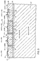
- FIG. 3 shows a sectional illustration of the SOI wafer, enlarged on a scale 10 after trench isolation and production of CMOS components.
- Vertical insulation regions 28 are introduced into the active silicon layer 26, which extend from the top 30 of the active silicon layer 26 to Lateral insulation layer 24 extend and the isolation of individual areas 32 of the active silicon layer 26 serve in the lateral extent.
- the Lateral or The width of the vertical insulation regions 28 is between 0.6 up to 2 ⁇ m.
- the Standard CMOS process various components, e.g. a high-voltage p-MOS 34, a high-voltage n-MOS 36, a logic p-MOS 38 and a logic n-MoS 40 educated.
- the high-voltage p-MOS 34 is in a diffused HV-n well 42 introduced that fills the entire area 32. That is this area 32 completely dielectric isolated. A p-n transition of this area 32 in Direction to the vertical isolation regions 28 and the boundary Lateral insulation layer 24 therefore does not exist. Also the area 32 in which the logic p-MOS 38 is formed is completely of an HV-n well 44 filled out into this area 32 a flat logic n well 46 in which the logic p-MOS 38 is located. The logic n MOS 40 is located in a flat logic p-well 48 that is in the isolated p-area 32 is introduced. Finally, the HV-n-MOS 36 is isolated p-area 32 introduced.
Landscapes
- Metal-Oxide And Bipolar Metal-Oxide Semiconductor Integrated Circuits (AREA)
- Element Separation (AREA)
Abstract
Description
- Parasitäreffekte, wie z.B. Latch-Up werden vollständig unterdrückt.
- In Leistungsschaltern generierte Minoritäten können keine Störungen in benachbarten Schaltungsteilen (z. B. Logik) erzeugen.
- Freie, d.h. vom Substrat entkoppelte, Bauelemente, wie z.B. Dioden, bieten neue Möglichkeiten in der Schaltungsentwicklung.
- ein SOI-Wafersubstrat verwendet wird, das eine obere Substratschicht zur Ausbildung der CMOS-Bauelemente, eine darunter angeordnete Lateral-Isolationsschicht und eine unter dieser angeordnete Trägerschicht aufweist,
- wobei die obere Substratschicht eine Dicke aufweist, die kleiner als oder gleich der größten Wannentiefe des CMOS-Prozesses ist,
- in die obere Substratschicht bis zur darunterliegenden Lateral-Isolationsschicht Vertikal-Isolationsgebiete eingebracht werden und
- innerhalb der zwischen den Vertikal-Isolationsgebieten liegenden Bereiche der Siliziumschicht mittels des CMOS-Prozesses Bauelemente ausgebildet werden, wobei sich die Wannen mit der größten Tiefe (Hochvolt-n-Wanne) bis zur Isolationsschicht erstrecken, und in diese Wannen größter Tiefe (Hochvolt-n-Wanne) direkt Bauelemente integriert werden können, während für Bauelemente, die eine geringere Wannentiefe benötigen, die diese Bauelemente umgebenden Wannen (Logik-n-Wanne) in Wannen größter Tiefe (Hochvolt-n-Wanne) eingebracht werden.
- Fig. 1
- ein Ablaufschema des erfindungsgemäßen Herstellungsprozesses mit dem Trenchmodul als Vorstufe für einen Standard-CMOS-Prozess,
- Fig. 2
- ein SOI-Wafersubstrat und
- Fig. 3
- Beispiele für CMOS-Bauelemente in der aktiven Siliziumschicht des SOI-Wafersubstrats.
Claims (3)
- Verfahren zur Herstellung einer IC-Schaltung mittels eines CMOS-Prozesses, insbesondere Hochvolt-CMOS-Prozesses, bei dem Bauelemente innerhalb von unterschiedlich tiefen Wannen von einem ersten Leitungstyp, insbesondere n-Wannen, ausgebildet werden, die in einer Substratschicht von einem dem ersten Leitungstyp entgegengesetzten zweiten Leitungstyp, insbesondere in ein p-Substrat, eingebracht werden, wobei bei dem Verfahrenein SOI-Wafersubstrat (10) verwendet wird, das eine obere Substratschicht (26) zur Ausbildung der CMOS-Bauelemente (34-40), eine darunter angeordnete Lateral-Isolationsschicht (24) und eine unter dieser angeordnete Trägerschicht (22) aufweist,wobei die obere Substratschicht (26) eine Dicke aufweist, die kleiner als oder gleich der größten Wannentiefe des CMOS-Prozesses ist,in die obere Substratschicht (26) bis zur darunterliegenden Lateral-Isolationsschicht (24) Vertikal-Isolationsgebiete (28) eingebracht werden undinnerhalb der zwischen den Vertikal-Isolationsgebieten (28) liegenden Bereiche (32) der Substratschicht (26) mittels des CMOS-Prozesses Bauelemente (34-40) ausgebildet werden, wobei sich die Wannen (42,44) mit der größten Tiefe (HV-n-Wanne) bis zur Isolationsschicht (24) erstrecken und den jeweiligen Bereich (32) vollständig ausfüllen, und in diese Wannen (42,44) größter Tiefe (HV-n-Wanne) direkt Bauelemente (34,36) integriert werden, während für Bauelemente (38,40), die eine geringere Wannentiefe benötigen, die diese Bauelemente (38,40) umgebenden Wannen (46,48) (Logik-n-Wanne) in Wannen (42,44) größter Tiefe (HV-n-Wanne) eingebracht werden.
- Verfahren nach Anspruch 1, dadurch gekennzeichnet, dass die Vertikal-Isolationsgebiete (28) durch Vertikal-Ätzung eines Trench in die Substratschicht (26) bis zur Lateral-Isolationsschicht (24) und durch anschließendes Einbringen oder Ausbilden eines Isolationsmaterials in dem Trench erzeugt werden.
- IC-Schaltung mit CMOS-Bauelementen (34-40), die nach Anspruch 1 oder 2 hergestellt sind.
Priority Applications (1)
| Application Number | Priority Date | Filing Date | Title |
|---|---|---|---|
| EP00114377A EP1067600B1 (de) | 1999-07-06 | 2000-07-05 | CMOS kompatibler SOI-Prozess |
Applications Claiming Priority (5)
| Application Number | Priority Date | Filing Date | Title |
|---|---|---|---|
| DE19931030 | 1999-07-06 | ||
| DE19931030 | 1999-07-06 | ||
| EP99121430 | 1999-10-27 | ||
| EP99121430 | 1999-10-27 | ||
| EP00114377A EP1067600B1 (de) | 1999-07-06 | 2000-07-05 | CMOS kompatibler SOI-Prozess |
Publications (2)
| Publication Number | Publication Date |
|---|---|
| EP1067600A1 true EP1067600A1 (de) | 2001-01-10 |
| EP1067600B1 EP1067600B1 (de) | 2006-11-02 |
Family
ID=27219209
Family Applications (1)
| Application Number | Title | Priority Date | Filing Date |
|---|---|---|---|
| EP00114377A Expired - Lifetime EP1067600B1 (de) | 1999-07-06 | 2000-07-05 | CMOS kompatibler SOI-Prozess |
Country Status (1)
| Country | Link |
|---|---|
| EP (1) | EP1067600B1 (de) |
Cited By (2)
| Publication number | Priority date | Publication date | Assignee | Title |
|---|---|---|---|---|
| DE10324066A1 (de) * | 2003-05-27 | 2004-12-30 | Texas Instruments Deutschland Gmbh | Stapelkondensator und Verfahren zur Herstellung eines solchen |
| EP1339101A3 (de) * | 2002-02-22 | 2005-11-30 | Xerox Corporation | Systeme und Verfahren zur Integration von heterogenen Schaltkreis-Bauelementen |
Citations (6)
| Publication number | Priority date | Publication date | Assignee | Title |
|---|---|---|---|---|
| JPH05291574A (ja) * | 1992-04-10 | 1993-11-05 | Fujitsu Ltd | 半導体装置 |
| EP0570043A2 (de) * | 1992-05-15 | 1993-11-18 | International Business Machines Corporation | SOI-Scheibe für BICMOS mit dünnen und dicken SOI-Siliziumgebieten |
| JPH08306893A (ja) * | 1995-04-28 | 1996-11-22 | Nippondenso Co Ltd | 半導体装置およびその製造方法 |
| US5708287A (en) * | 1995-11-29 | 1998-01-13 | Kabushiki Kaisha Toshiba | Power semiconductor device having an active layer |
| JPH10107288A (ja) * | 1996-09-26 | 1998-04-24 | Matsushita Electric Works Ltd | 半導体装置 |
| DE19732237A1 (de) * | 1997-01-10 | 1998-07-16 | Nat Semiconductor Corp | Mehrschichtiger Wafer |
-
2000
- 2000-07-05 EP EP00114377A patent/EP1067600B1/de not_active Expired - Lifetime
Patent Citations (6)
| Publication number | Priority date | Publication date | Assignee | Title |
|---|---|---|---|---|
| JPH05291574A (ja) * | 1992-04-10 | 1993-11-05 | Fujitsu Ltd | 半導体装置 |
| EP0570043A2 (de) * | 1992-05-15 | 1993-11-18 | International Business Machines Corporation | SOI-Scheibe für BICMOS mit dünnen und dicken SOI-Siliziumgebieten |
| JPH08306893A (ja) * | 1995-04-28 | 1996-11-22 | Nippondenso Co Ltd | 半導体装置およびその製造方法 |
| US5708287A (en) * | 1995-11-29 | 1998-01-13 | Kabushiki Kaisha Toshiba | Power semiconductor device having an active layer |
| JPH10107288A (ja) * | 1996-09-26 | 1998-04-24 | Matsushita Electric Works Ltd | 半導体装置 |
| DE19732237A1 (de) * | 1997-01-10 | 1998-07-16 | Nat Semiconductor Corp | Mehrschichtiger Wafer |
Non-Patent Citations (3)
| Title |
|---|
| PATENT ABSTRACTS OF JAPAN vol. 018, no. 080 (E - 1505) 9 February 1994 (1994-02-09) * |
| PATENT ABSTRACTS OF JAPAN vol. 1997, no. 03 31 March 1997 (1997-03-31) * |
| PATENT ABSTRACTS OF JAPAN vol. 1998, no. 09 31 July 1998 (1998-07-31) * |
Cited By (6)
| Publication number | Priority date | Publication date | Assignee | Title |
|---|---|---|---|---|
| EP1339101A3 (de) * | 2002-02-22 | 2005-11-30 | Xerox Corporation | Systeme und Verfahren zur Integration von heterogenen Schaltkreis-Bauelementen |
| US7341930B2 (en) | 2002-02-22 | 2008-03-11 | Xerox Corporation | Systems and methods for integration of heterogeneous circuit devices |
| US7352047B2 (en) | 2002-02-22 | 2008-04-01 | Xerox Corporation | Systems and methods for integration of heterogeneous circuit devices |
| DE10324066A1 (de) * | 2003-05-27 | 2004-12-30 | Texas Instruments Deutschland Gmbh | Stapelkondensator und Verfahren zur Herstellung eines solchen |
| US7130182B2 (en) | 2003-05-27 | 2006-10-31 | Texas Instruments Incorporated | Stacked capacitor and method for fabricating same |
| US7312119B2 (en) | 2003-05-27 | 2007-12-25 | Texas Instruments Incorporated | Stacked capacitor and method of fabricating same |
Also Published As
| Publication number | Publication date |
|---|---|
| EP1067600B1 (de) | 2006-11-02 |
Similar Documents
| Publication | Publication Date | Title |
|---|---|---|
| DE102008034158B4 (de) | Integrierte Schaltungen mit einer Halbleiteranordnung in Dünnfilm-SOI-Technologie und Verfahren zur Herstellung derselben | |
| DE102004014923A1 (de) | Verfahren zum Bereitstellen einer Dreifach-Wanne in einem epitaktisch basierten CMOS- oder BiCMOS-Prozess | |
| DE19520958C2 (de) | Halbleitervorrichtung mit Wannenbereichen und Verfahren zur Herstellung der Halbleitervorrichtung | |
| DE3334337A1 (de) | Verfahren zur herstellung einer integrierten halbleitereinrichtung | |
| DE102007034803B4 (de) | Halbleiterbauelement mit integriertem Hall-Effekt-Sensor | |
| DE69530441T2 (de) | Eine Methode zur Herstellung von BiCMOS-Halbleiterteilen | |
| DE112011100605T5 (de) | Integriertes hall-effekt-element mit germanium-hall-platte | |
| DE69231484T2 (de) | Verfahren zur Herstellung von Isolationszonen des LOCOS-Typs für integrierte Schaltungen vom MOS-Typ | |
| DE10300577A1 (de) | Verfahren zur Herstellung eines Halbleiterbauelements | |
| EP1631990B1 (de) | Herstellungsverfahren für einen feldeffekttransistor | |
| DE4139039A1 (de) | Halbleitervorrichtung | |
| DE102013225362A1 (de) | Erhöhen der durchbruchsspannung einer metalloxidhalbleitereinrichtung | |
| EP1794803A2 (de) | Lateraler dmos-transistor und verfahren zu seiner herstellung | |
| DE10116800A1 (de) | Halbleitervorrichtung und Verfahren zu ihrer Herstellung | |
| DE19647324B4 (de) | Halbleiterbauelement | |
| DE3842749A1 (de) | Verfahren zum herstellen einer integrierten schaltung | |
| DE69333098T2 (de) | Integriertes Halbleiterschaltkreisbauelement und dessen Herstellungsverfahren | |
| EP1067600B1 (de) | CMOS kompatibler SOI-Prozess | |
| DE102004036387B4 (de) | Hochvolt-MOS-Transistor und entsprechendes Herstellungsverfahren | |
| WO2008116875A1 (de) | Bipolarintegration ohne zusätzliche maskenschritte | |
| EP0843888B1 (de) | Verfahren zur herstellung eines selbstjustierten kontaktes und eines dotierten bereichs | |
| DE102024121608B4 (de) | Halbleitervorrichtung | |
| DE10343132B4 (de) | Isolierte MOS-Transistoren mit ausgedehntem Drain-Gebiet für erhöhte Spannungen | |
| DE19928795C2 (de) | Kombinierte LV/HV-Technologie mit retrograd dotierter Drain-Extension für HV-Transistoren | |
| EP0967657B1 (de) | NMOS-Transistor |
Legal Events
| Date | Code | Title | Description |
|---|---|---|---|
| PUAI | Public reference made under article 153(3) epc to a published international application that has entered the european phase |
Free format text: ORIGINAL CODE: 0009012 |
|
| AK | Designated contracting states |
Kind code of ref document: A1 Designated state(s): AT BE CH CY DE DK ES FI FR GB GR IE IT LI LU MC NL PT SE |
|
| AX | Request for extension of the european patent |
Free format text: AL;LT;LV;MK;RO;SI |
|
| 17P | Request for examination filed |
Effective date: 20010110 |
|
| AKX | Designation fees paid |
Free format text: AT BE CH CY DE DK ES FI FR GB GR IE IT LI LU MC NL PT SE |
|
| GRAP | Despatch of communication of intention to grant a patent |
Free format text: ORIGINAL CODE: EPIDOSNIGR1 |
|
| GRAS | Grant fee paid |
Free format text: ORIGINAL CODE: EPIDOSNIGR3 |
|
| GRAA | (expected) grant |
Free format text: ORIGINAL CODE: 0009210 |
|
| AK | Designated contracting states |
Kind code of ref document: B1 Designated state(s): AT BE CH CY DE DK ES FI FR GB GR IE IT LI LU MC NL PT SE |
|
| PG25 | Lapsed in a contracting state [announced via postgrant information from national office to epo] |
Ref country code: FI Free format text: LAPSE BECAUSE OF FAILURE TO SUBMIT A TRANSLATION OF THE DESCRIPTION OR TO PAY THE FEE WITHIN THE PRESCRIBED TIME-LIMIT Effective date: 20061102 |
|
| REG | Reference to a national code |
Ref country code: GB Ref legal event code: FG4D Free format text: NOT ENGLISH |
|
| REG | Reference to a national code |
Ref country code: IE Ref legal event code: FG4D Free format text: LANGUAGE OF EP DOCUMENT: GERMAN |
|
| REG | Reference to a national code |
Ref country code: CH Ref legal event code: EP |
|
| REF | Corresponds to: |
Ref document number: 50013674 Country of ref document: DE Date of ref document: 20061214 Kind code of ref document: P |
|
| REG | Reference to a national code |
Ref country code: CH Ref legal event code: NV Representative=s name: HEPP, WENGER & RYFFEL AG |
|
| PG25 | Lapsed in a contracting state [announced via postgrant information from national office to epo] |
Ref country code: SE Free format text: LAPSE BECAUSE OF FAILURE TO SUBMIT A TRANSLATION OF THE DESCRIPTION OR TO PAY THE FEE WITHIN THE PRESCRIBED TIME-LIMIT Effective date: 20070202 Ref country code: DK Free format text: LAPSE BECAUSE OF FAILURE TO SUBMIT A TRANSLATION OF THE DESCRIPTION OR TO PAY THE FEE WITHIN THE PRESCRIBED TIME-LIMIT Effective date: 20070202 |
|
| PG25 | Lapsed in a contracting state [announced via postgrant information from national office to epo] |
Ref country code: ES Free format text: LAPSE BECAUSE OF FAILURE TO SUBMIT A TRANSLATION OF THE DESCRIPTION OR TO PAY THE FEE WITHIN THE PRESCRIBED TIME-LIMIT Effective date: 20070213 |
|
| GBT | Gb: translation of ep patent filed (gb section 77(6)(a)/1977) |
Effective date: 20070129 |
|
| PG25 | Lapsed in a contracting state [announced via postgrant information from national office to epo] |
Ref country code: PT Free format text: LAPSE BECAUSE OF FAILURE TO SUBMIT A TRANSLATION OF THE DESCRIPTION OR TO PAY THE FEE WITHIN THE PRESCRIBED TIME-LIMIT Effective date: 20070402 |
|
| ET | Fr: translation filed | ||
| PLBE | No opposition filed within time limit |
Free format text: ORIGINAL CODE: 0009261 |
|
| STAA | Information on the status of an ep patent application or granted ep patent |
Free format text: STATUS: NO OPPOSITION FILED WITHIN TIME LIMIT |
|
| 26N | No opposition filed |
Effective date: 20070803 |
|
| PG25 | Lapsed in a contracting state [announced via postgrant information from national office to epo] |
Ref country code: MC Free format text: LAPSE BECAUSE OF NON-PAYMENT OF DUE FEES Effective date: 20070731 Ref country code: GR Free format text: LAPSE BECAUSE OF FAILURE TO SUBMIT A TRANSLATION OF THE DESCRIPTION OR TO PAY THE FEE WITHIN THE PRESCRIBED TIME-LIMIT Effective date: 20070203 |
|
| PG25 | Lapsed in a contracting state [announced via postgrant information from national office to epo] |
Ref country code: CY Free format text: LAPSE BECAUSE OF FAILURE TO SUBMIT A TRANSLATION OF THE DESCRIPTION OR TO PAY THE FEE WITHIN THE PRESCRIBED TIME-LIMIT Effective date: 20061102 Ref country code: LU Free format text: LAPSE BECAUSE OF NON-PAYMENT OF DUE FEES Effective date: 20070705 |
|
| REG | Reference to a national code |
Ref country code: DE Ref legal event code: R082 Ref document number: 50013674 Country of ref document: DE Representative=s name: VON KREISLER SELTING WERNER - PARTNERSCHAFT VO, DE |
|
| REG | Reference to a national code |
Ref country code: DE Ref legal event code: R081 Ref document number: 50013674 Country of ref document: DE Owner name: ELMOS SEMICONDUCTOR AKTIENGESELLSCHAFT, DE Free format text: FORMER OWNER: ELMOS SEMICONDUCTOR AG, 44227 DORTMUND, DE Effective date: 20150108 Ref country code: DE Ref legal event code: R082 Ref document number: 50013674 Country of ref document: DE Representative=s name: VON KREISLER SELTING WERNER - PARTNERSCHAFT VO, DE Effective date: 20150108 Ref country code: DE Ref legal event code: R082 Ref document number: 50013674 Country of ref document: DE Representative=s name: DOMPATENT VON KREISLER SELTING WERNER - PARTNE, DE Effective date: 20150108 |
|
| REG | Reference to a national code |
Ref country code: FR Ref legal event code: PLFP Year of fee payment: 17 |
|
| REG | Reference to a national code |
Ref country code: FR Ref legal event code: PLFP Year of fee payment: 18 |
|
| REG | Reference to a national code |
Ref country code: FR Ref legal event code: PLFP Year of fee payment: 19 |
|
| PGFP | Annual fee paid to national office [announced via postgrant information from national office to epo] |
Ref country code: NL Payment date: 20190722 Year of fee payment: 20 |
|
| PGFP | Annual fee paid to national office [announced via postgrant information from national office to epo] |
Ref country code: DE Payment date: 20190723 Year of fee payment: 20 Ref country code: IE Payment date: 20190725 Year of fee payment: 20 Ref country code: IT Payment date: 20190723 Year of fee payment: 20 Ref country code: FR Payment date: 20190724 Year of fee payment: 20 |
|
| PGFP | Annual fee paid to national office [announced via postgrant information from national office to epo] |
Ref country code: BE Payment date: 20190722 Year of fee payment: 20 |
|
| PGFP | Annual fee paid to national office [announced via postgrant information from national office to epo] |
Ref country code: AT Payment date: 20190719 Year of fee payment: 20 Ref country code: GB Payment date: 20190725 Year of fee payment: 20 |
|
| PGFP | Annual fee paid to national office [announced via postgrant information from national office to epo] |
Ref country code: CH Payment date: 20190725 Year of fee payment: 20 |
|
| REG | Reference to a national code |
Ref country code: DE Ref legal event code: R071 Ref document number: 50013674 Country of ref document: DE |
|
| REG | Reference to a national code |
Ref country code: NL Ref legal event code: MK Effective date: 20200704 |
|
| REG | Reference to a national code |
Ref country code: CH Ref legal event code: PL |
|
| REG | Reference to a national code |
Ref country code: GB Ref legal event code: PE20 Expiry date: 20200704 |
|
| REG | Reference to a national code |
Ref country code: DE Ref legal event code: R082 Ref document number: 50013674 Country of ref document: DE Representative=s name: DOMPATENT VON KREISLER SELTING WERNER - PARTNE, DE Ref country code: DE Ref legal event code: R081 Ref document number: 50013674 Country of ref document: DE Owner name: ELMOS SEMICONDUCTOR SE, DE Free format text: FORMER OWNER: ELMOS SEMICONDUCTOR AKTIENGESELLSCHAFT, 44227 DORTMUND, DE |
|
| REG | Reference to a national code |
Ref country code: AT Ref legal event code: MK07 Ref document number: 344535 Country of ref document: AT Kind code of ref document: T Effective date: 20200705 |
|
| REG | Reference to a national code |
Ref country code: BE Ref legal event code: MK Effective date: 20200705 |
|
| REG | Reference to a national code |
Ref country code: IE Ref legal event code: MK9A |
|
| PG25 | Lapsed in a contracting state [announced via postgrant information from national office to epo] |
Ref country code: IE Free format text: LAPSE BECAUSE OF EXPIRATION OF PROTECTION Effective date: 20200705 Ref country code: GB Free format text: LAPSE BECAUSE OF EXPIRATION OF PROTECTION Effective date: 20200704 |