EP1067598A1 - Method of packaging semiconductor device using anisotropic conductive adhesive - Google Patents
Method of packaging semiconductor device using anisotropic conductive adhesive Download PDFInfo
- Publication number
- EP1067598A1 EP1067598A1 EP00901937A EP00901937A EP1067598A1 EP 1067598 A1 EP1067598 A1 EP 1067598A1 EP 00901937 A EP00901937 A EP 00901937A EP 00901937 A EP00901937 A EP 00901937A EP 1067598 A1 EP1067598 A1 EP 1067598A1
- Authority
- EP
- European Patent Office
- Prior art keywords
- semiconductor device
- circuit board
- anisotropic conductive
- mounting
- adhesive resin
- Prior art date
- Legal status (The legal status is an assumption and is not a legal conclusion. Google has not performed a legal analysis and makes no representation as to the accuracy of the status listed.)
- Granted
Links
Images




Classifications
-
- H—ELECTRICITY
- H05—ELECTRIC TECHNIQUES NOT OTHERWISE PROVIDED FOR
- H05K—PRINTED CIRCUITS; CASINGS OR CONSTRUCTIONAL DETAILS OF ELECTRIC APPARATUS; MANUFACTURE OF ASSEMBLAGES OF ELECTRICAL COMPONENTS
- H05K3/00—Apparatus or processes for manufacturing printed circuits
- H05K3/30—Assembling printed circuits with electric components, e.g. with resistors
- H05K3/32—Assembling printed circuits with electric components, e.g. with resistors electrically connecting electric components or wires to printed circuits
- H05K3/321—Assembling printed circuits with electric components, e.g. with resistors electrically connecting electric components or wires to printed circuits by conductive adhesives
- H05K3/323—Assembling printed circuits with electric components, e.g. with resistors electrically connecting electric components or wires to printed circuits by conductive adhesives by applying an anisotropic conductive adhesive layer over an array of pads
-
- H—ELECTRICITY
- H05—ELECTRIC TECHNIQUES NOT OTHERWISE PROVIDED FOR
- H05K—PRINTED CIRCUITS; CASINGS OR CONSTRUCTIONAL DETAILS OF ELECTRIC APPARATUS; MANUFACTURE OF ASSEMBLAGES OF ELECTRICAL COMPONENTS
- H05K3/00—Apparatus or processes for manufacturing printed circuits
- H05K3/30—Assembling printed circuits with electric components, e.g. with resistors
- H05K3/32—Assembling printed circuits with electric components, e.g. with resistors electrically connecting electric components or wires to printed circuits
-
- H—ELECTRICITY
- H05—ELECTRIC TECHNIQUES NOT OTHERWISE PROVIDED FOR
- H05K—PRINTED CIRCUITS; CASINGS OR CONSTRUCTIONAL DETAILS OF ELECTRIC APPARATUS; MANUFACTURE OF ASSEMBLAGES OF ELECTRICAL COMPONENTS
- H05K2201/00—Indexing scheme relating to printed circuits covered by H05K1/00
- H05K2201/09—Shape and layout
- H05K2201/09209—Shape and layout details of conductors
- H05K2201/09654—Shape and layout details of conductors covering at least two types of conductors provided for in H05K2201/09218 - H05K2201/095
- H05K2201/09781—Dummy conductors, i.e. not used for normal transport of current; Dummy electrodes of components
-
- H—ELECTRICITY
- H05—ELECTRIC TECHNIQUES NOT OTHERWISE PROVIDED FOR
- H05K—PRINTED CIRCUITS; CASINGS OR CONSTRUCTIONAL DETAILS OF ELECTRIC APPARATUS; MANUFACTURE OF ASSEMBLAGES OF ELECTRICAL COMPONENTS
- H05K2201/00—Indexing scheme relating to printed circuits covered by H05K1/00
- H05K2201/10—Details of components or other objects attached to or integrated in a printed circuit board
- H05K2201/10613—Details of electrical connections of non-printed components, e.g. special leads
- H05K2201/10621—Components characterised by their electrical contacts
- H05K2201/10674—Flip chip
-
- H—ELECTRICITY
- H05—ELECTRIC TECHNIQUES NOT OTHERWISE PROVIDED FOR
- H05K—PRINTED CIRCUITS; CASINGS OR CONSTRUCTIONAL DETAILS OF ELECTRIC APPARATUS; MANUFACTURE OF ASSEMBLAGES OF ELECTRICAL COMPONENTS
- H05K2203/00—Indexing scheme relating to apparatus or processes for manufacturing printed circuits covered by H05K3/00
- H05K2203/14—Related to the order of processing steps
- H05K2203/1476—Same or similar kind of process performed in phases, e.g. coarse patterning followed by fine patterning
-
- H—ELECTRICITY
- H05—ELECTRIC TECHNIQUES NOT OTHERWISE PROVIDED FOR
- H05K—PRINTED CIRCUITS; CASINGS OR CONSTRUCTIONAL DETAILS OF ELECTRIC APPARATUS; MANUFACTURE OF ASSEMBLAGES OF ELECTRICAL COMPONENTS
- H05K2203/00—Indexing scheme relating to apparatus or processes for manufacturing printed circuits covered by H05K3/00
- H05K2203/16—Inspection; Monitoring; Aligning
- H05K2203/166—Alignment or registration; Control of registration
-
- H—ELECTRICITY
- H05—ELECTRIC TECHNIQUES NOT OTHERWISE PROVIDED FOR
- H05K—PRINTED CIRCUITS; CASINGS OR CONSTRUCTIONAL DETAILS OF ELECTRIC APPARATUS; MANUFACTURE OF ASSEMBLAGES OF ELECTRICAL COMPONENTS
- H05K3/00—Apparatus or processes for manufacturing printed circuits
- H05K3/30—Assembling printed circuits with electric components, e.g. with resistors
- H05K3/32—Assembling printed circuits with electric components, e.g. with resistors electrically connecting electric components or wires to printed circuits
- H05K3/34—Assembling printed circuits with electric components, e.g. with resistors electrically connecting electric components or wires to printed circuits by soldering
- H05K3/3494—Heating processes for reflow soldering
-
- H—ELECTRICITY
- H10—SEMICONDUCTOR DEVICES; ELECTRIC SOLID-STATE DEVICES NOT OTHERWISE PROVIDED FOR
- H10W—GENERIC PACKAGES, INTERCONNECTIONS, CONNECTORS OR OTHER CONSTRUCTIONAL DETAILS OF DEVICES COVERED BY CLASS H10
- H10W72/00—Interconnections or connectors in packages
- H10W72/071—Connecting or disconnecting
- H10W72/072—Connecting or disconnecting of bump connectors
-
- H—ELECTRICITY
- H10—SEMICONDUCTOR DEVICES; ELECTRIC SOLID-STATE DEVICES NOT OTHERWISE PROVIDED FOR
- H10W—GENERIC PACKAGES, INTERCONNECTIONS, CONNECTORS OR OTHER CONSTRUCTIONAL DETAILS OF DEVICES COVERED BY CLASS H10
- H10W72/00—Interconnections or connectors in packages
- H10W72/071—Connecting or disconnecting
- H10W72/073—Connecting or disconnecting of die-attach connectors
-
- H—ELECTRICITY
- H10—SEMICONDUCTOR DEVICES; ELECTRIC SOLID-STATE DEVICES NOT OTHERWISE PROVIDED FOR
- H10W—GENERIC PACKAGES, INTERCONNECTIONS, CONNECTORS OR OTHER CONSTRUCTIONAL DETAILS OF DEVICES COVERED BY CLASS H10
- H10W72/00—Interconnections or connectors in packages
- H10W72/071—Connecting or disconnecting
- H10W72/073—Connecting or disconnecting of die-attach connectors
- H10W72/07331—Connecting techniques
- H10W72/07337—Connecting techniques using a polymer adhesive, e.g. an adhesive based on silicone or epoxy
- H10W72/07338—Connecting techniques using a polymer adhesive, e.g. an adhesive based on silicone or epoxy hardening the adhesive by curing, e.g. thermosetting
-
- H—ELECTRICITY
- H10—SEMICONDUCTOR DEVICES; ELECTRIC SOLID-STATE DEVICES NOT OTHERWISE PROVIDED FOR
- H10W—GENERIC PACKAGES, INTERCONNECTIONS, CONNECTORS OR OTHER CONSTRUCTIONAL DETAILS OF DEVICES COVERED BY CLASS H10
- H10W72/00—Interconnections or connectors in packages
- H10W72/071—Connecting or disconnecting
- H10W72/073—Connecting or disconnecting of die-attach connectors
- H10W72/07341—Controlling the bonding environment, e.g. atmosphere composition or temperature
-
- H—ELECTRICITY
- H10—SEMICONDUCTOR DEVICES; ELECTRIC SOLID-STATE DEVICES NOT OTHERWISE PROVIDED FOR
- H10W—GENERIC PACKAGES, INTERCONNECTIONS, CONNECTORS OR OTHER CONSTRUCTIONAL DETAILS OF DEVICES COVERED BY CLASS H10
- H10W72/00—Interconnections or connectors in packages
- H10W72/071—Connecting or disconnecting
- H10W72/074—Connecting or disconnecting of anisotropic conductive adhesives
-
- H—ELECTRICITY
- H10—SEMICONDUCTOR DEVICES; ELECTRIC SOLID-STATE DEVICES NOT OTHERWISE PROVIDED FOR
- H10W—GENERIC PACKAGES, INTERCONNECTIONS, CONNECTORS OR OTHER CONSTRUCTIONAL DETAILS OF DEVICES COVERED BY CLASS H10
- H10W72/00—Interconnections or connectors in packages
- H10W72/20—Bump connectors, e.g. solder bumps or copper pillars; Dummy bumps; Thermal bumps
- H10W72/241—Dispositions, e.g. layouts
-
- H—ELECTRICITY
- H10—SEMICONDUCTOR DEVICES; ELECTRIC SOLID-STATE DEVICES NOT OTHERWISE PROVIDED FOR
- H10W—GENERIC PACKAGES, INTERCONNECTIONS, CONNECTORS OR OTHER CONSTRUCTIONAL DETAILS OF DEVICES COVERED BY CLASS H10
- H10W72/00—Interconnections or connectors in packages
- H10W72/30—Die-attach connectors
- H10W72/321—Structures or relative sizes of die-attach connectors
- H10W72/325—Die-attach connectors having a filler embedded in a matrix
-
- H—ELECTRICITY
- H10—SEMICONDUCTOR DEVICES; ELECTRIC SOLID-STATE DEVICES NOT OTHERWISE PROVIDED FOR
- H10W—GENERIC PACKAGES, INTERCONNECTIONS, CONNECTORS OR OTHER CONSTRUCTIONAL DETAILS OF DEVICES COVERED BY CLASS H10
- H10W72/00—Interconnections or connectors in packages
- H10W72/30—Die-attach connectors
- H10W72/351—Materials of die-attach connectors
- H10W72/352—Materials of die-attach connectors comprising metals or metalloids, e.g. solders
-
- H—ELECTRICITY
- H10—SEMICONDUCTOR DEVICES; ELECTRIC SOLID-STATE DEVICES NOT OTHERWISE PROVIDED FOR
- H10W—GENERIC PACKAGES, INTERCONNECTIONS, CONNECTORS OR OTHER CONSTRUCTIONAL DETAILS OF DEVICES COVERED BY CLASS H10
- H10W72/00—Interconnections or connectors in packages
- H10W72/30—Die-attach connectors
- H10W72/351—Materials of die-attach connectors
- H10W72/353—Materials of die-attach connectors not comprising solid metals or solid metalloids, e.g. ceramics
- H10W72/354—Materials of die-attach connectors not comprising solid metals or solid metalloids, e.g. ceramics comprising polymers
-
- H—ELECTRICITY
- H10—SEMICONDUCTOR DEVICES; ELECTRIC SOLID-STATE DEVICES NOT OTHERWISE PROVIDED FOR
- H10W—GENERIC PACKAGES, INTERCONNECTIONS, CONNECTORS OR OTHER CONSTRUCTIONAL DETAILS OF DEVICES COVERED BY CLASS H10
- H10W72/00—Interconnections or connectors in packages
- H10W72/30—Die-attach connectors
- H10W72/351—Materials of die-attach connectors
- H10W72/355—Materials of die-attach connectors of outermost layers of multilayered die-attach connectors, e.g. material of a coating
-
- H—ELECTRICITY
- H10—SEMICONDUCTOR DEVICES; ELECTRIC SOLID-STATE DEVICES NOT OTHERWISE PROVIDED FOR
- H10W—GENERIC PACKAGES, INTERCONNECTIONS, CONNECTORS OR OTHER CONSTRUCTIONAL DETAILS OF DEVICES COVERED BY CLASS H10
- H10W74/00—Encapsulations, e.g. protective coatings
- H10W74/10—Encapsulations, e.g. protective coatings characterised by their shape or disposition
- H10W74/15—Encapsulations, e.g. protective coatings characterised by their shape or disposition on active surfaces of flip-chip devices, e.g. underfills
-
- H—ELECTRICITY
- H10—SEMICONDUCTOR DEVICES; ELECTRIC SOLID-STATE DEVICES NOT OTHERWISE PROVIDED FOR
- H10W—GENERIC PACKAGES, INTERCONNECTIONS, CONNECTORS OR OTHER CONSTRUCTIONAL DETAILS OF DEVICES COVERED BY CLASS H10
- H10W90/00—Package configurations
- H10W90/701—Package configurations characterised by the relative positions of pads or connectors relative to package parts
- H10W90/721—Package configurations characterised by the relative positions of pads or connectors relative to package parts of bump connectors
- H10W90/724—Package configurations characterised by the relative positions of pads or connectors relative to package parts of bump connectors between a chip and a stacked insulating package substrate, interposer or RDL
-
- H—ELECTRICITY
- H10—SEMICONDUCTOR DEVICES; ELECTRIC SOLID-STATE DEVICES NOT OTHERWISE PROVIDED FOR
- H10W—GENERIC PACKAGES, INTERCONNECTIONS, CONNECTORS OR OTHER CONSTRUCTIONAL DETAILS OF DEVICES COVERED BY CLASS H10
- H10W90/00—Package configurations
- H10W90/701—Package configurations characterised by the relative positions of pads or connectors relative to package parts
- H10W90/731—Package configurations characterised by the relative positions of pads or connectors relative to package parts of die-attach connectors
- H10W90/734—Package configurations characterised by the relative positions of pads or connectors relative to package parts of die-attach connectors between a chip and a stacked insulating package substrate, interposer or RDL
Definitions
- the present invention relates to a method of mounting a semiconductor device whereby the semiconductor device is connected with, and fixed to the surface of a circuit board with the use of an anisotropic conductive adhesive.
- a method of mounting a semiconductor device whereby the semiconductor device is connected with, and fixed to the surface of a circuit board with the use of an anisotropic conductive adhesive has been put to practical use.
- the conventional method of mounting a semiconductor device is described hereinafter with reference to Figs. 11 to 16.
- Figs. 11 to 14 are sectional views showing respective steps of the conventional method of mounting the semiconductor device.
- wiring patterns 15 provided on a circuit board 17 are connected with bumps 14 formed on a semiconductor device 16, respectively.
- conductive particles 12 having electric conductivity, contained in an anisotropic conductive adhesive 13 are sandwiched between the respective wiring patterns 15 and the respective bumps 14, thereby effecting electric conduction therebetween by the agency of the conductive particles 12.
- the anisotropic conductive adhesive 13 is composed of the conductive particles 12 which are mixed in an adhesive resin 11 of a thermosetting type, made of an epoxy based adhesive, so as to have electric conductivity, and is formed in a film-like shape on a base film while being protected by a cover film.
- the conductive particles 12 are metallic particles made of silver, solder, or so forth, 5 to 10 ⁇ m in diameter, or composed of resin particles made of a plastic, with gold (Au) plating applied on the surface thereof.
- the circuit board 17 is provided with the wiring patterns 15 formed on a substrate thereof, made of glass epoxy resin, ceramic, or glass.
- the wiring patterns 15 are formed of copper or gold, or composed of an indium tin oxide (ITO) film, or so forth for use in a liquid crystal display panel, and the like.
- An operation of mounting a semiconductor device comprises the following steps.
- the anisotropic conductive adhesive 13 is transferred onto a part of the circuit board 17 where the semiconductor device 16 is to be connected.
- the semiconductor device 16 is placed on the circuit board 17 disposed opposite thereto, after aligning the respective wiring patterns 15 provided on the circuit board 17 with the respective bumps 14 formed on the semiconductor device 16.
- the semiconductor device 16 is thermally press-bonded to the circuit board 17 by heating the semiconductor device 16 while applying a pressure P thereto by use of a heating and pressurizing tool 18 provided with a built-in heater as shown in Fig. 13, thereby curing the adhesive resin 11 contained in the anisotropic conductive adhesive 13.
- the semiconductor device 16 upon curing of the adhesive resin 11, the semiconductor device 16 is bonded to, and fixed to the surface of the circuit board 17, so that electric conduction is maintained between the respective bumps 14 of the semiconductor device 16, and the respective wiring patterns 15 through the intermediary of the conductive particles 12 contained in the anisotropic conductive adhesive 13.
- a thermal press-bonding process proceeds from the outset at a temperature required for curing the adhesive resin 11 by use of the heating and pressurizing tool 18, however, the adhesive resin 11 of the thermosetting type, such as an epoxy based adhesive, and so forth, softens up rapidly when heated to more than a certain temperature, and is turned into a half-fusion state. Thereafter, a curing reaction proceeds, thereby curing the adhesive resin 11.
- Figs. 15 and 16 are enlarged views showing conditions of a structure for mounting the semiconductor device before, and after the thermal press-bonding process, respectively.
- Fig. 15 shows the condition when the semiconductor device 16 is placed on the circuit board 17, that is, the condition before heating and pressurizing are carried out by use of the heating and pressurizing tool 18 as shown in Fig. 13, showing an enlarged view of a part of the semiconductor device 16, and the circuit board 17, respectively, so as to illustrate with clarity the state of the conductive particles 12 existing between the bumps 14 and the wiring patterns 15.
- the adhesive resin 11 remains in the film-like shape as transferred.
- the conductive particles 12 are also pushed out outside under the respective bumps 14, and consequently, when the thermal press-bonding process is completed upon curing of the adhesive resin 11 later on, many of the conductive particles 12 will be found to be present in regions lying off the bottom face of the respective bumps 14. Accordingly, there will remain only a few of the conductive particles 12 between the respective bumps 14 and the respective wiring patterns 15.
- the invention has been developed to solve such a problem as described above with the conventional method of mounting the semiconductor device using the anisotropic conductive adhesive, and it is therefore an object of the invention to enable stable connection to be effected at low connecting resistance even if the area of the connecting region is small by increasing the number of conductive particles arrested between the respective bumps of the semiconductor device and the respective wiring patterns of the circuit board, thereby rendering the method suitable for high-density mounting.
- the method of mounting a semiconductor device using an anisotropic conductive adhesive comprises the following steps (1) to (4).
- electric conduction is preferably effected between the bumps of the semiconductor device and the wiring patterns of the circuit board, respectively, in the step of provisionally press-bonding the semiconductor device onto the circuit board.
- step described under (4) may be performed by means of thermal press-bonding using a heating and pressurizing tool set at a temperature causing the adhesive resin to be cured.
- the step described under (4) may be performed by placing the circuit board with the semiconductor device provisionally press-bonded thereto in a furnace set at a temperature causing the adhesive resin to be cured, or by placing the circuit board with the semiconductor device provisionally press-bonded thereto on a hot plate set at the temperature causing the adhesive resin to be cured.
- the conductive particles are preferably brought into contact with the bumps of the semiconductor device and the wiring patterns of the circuit board, respectively.
- Fig. 1 is an enlarged schematic sectional view showing a part of an anisotropic conductive adhesive for use in the method of mounting the semiconductor device according to the invention.
- the anisotropic conductive adhesive is formed in a film-like shape before use on top of a base film, and a surface of the opposite side thereof is protected by a cover film although illustration thereof is omitted.
- the anisotropic conductive adhesive 13 is composed of a multitude of conductive particles 12 in the range of 3 to several tens of pm in diameter which are mixed in a film of an adhesive resin 11, in the order of 15 to 100 ⁇ m in thickness, having a construction provided with electric conductivity in thickness direction.
- the film of the adhesive resin 11 is set to a thickness in the order of 15 to 100 ⁇ m, however, a specific thickness thereof is decided upon according to a height (height from a substrate) of bumps 14 formed on a semiconductor device 16 to be mounted and a height (height from a substrate) of wiring patterns 15 provided on a circuit board 17, as shown in Figs. 6 and so forth.
- a thickness in excess of a height (thickness) equivalent to the sum of heights of both elements described and accordingly, is set to have a thickness of 38 ⁇ m or more, that is, the sum of both the elements.
- the adhesive resin is formed in a film-like shape by the printing method or the transfer method, however, in practice, the film of the adhesive resin is formed to a thickness thicker by about 10 ⁇ m than the thickness described above, taking into account accuracy in forming the same. Accordingly, in the above-mentioned case, the film of the adhesive resin 11 is formed to a thickness in the order of 50 ⁇ m, thicker by about 10 ⁇ m than 38 ⁇ m.
- an insulating and thermosetting resin such as an epoxy resin, a phenolic resin, and so forth, for example, an epoxy based thermosetting resin, is used.
- the conductive particles 12 to be mixed in the adhesive resin 11 are in the range of 3 to several tens of ⁇ m in diameter, and are metallic particles made of silver or solder, or resin particles made of a plastic, with gold (Au) plating applied on the surface thereof.
- the diameter of the conductive particles 12 varies depending on a gap (spacing) between the wiring patterns 15 to which the bumps are to be connected, respectively. For example, if the gap is 10 ⁇ m, the diameter of the conductive particles 12 is set at no more than 10 ⁇ m in order to prevent short-circuiting from occurring between the wiring patterns 15.
- the conductive particles 12 in an amount of 4 wt % (% by weight) are added to the adhesive resin 11, and a mixture is tempered, thereby forming the anisotropic conductive adhesive 13.
- the circuit board 17 shown in Fig. 2 and subsequent figures is provided with the wiring patterns 15 formed on a substrate thereof, made of a glass epoxy resin, ceramic, or glass.
- the wiring patterns 15 are formed of copper or gold, or composed of an indium tin oxide (ITO) film, or so forth for use in a liquid crystal display panel, and the like.
- An operation of mounting the semiconductor device 16 on the circuit board 17 comprises the following steps.
- the respective wiring patterns 15 provided on the circuit board 17 are connected with the respective bumps 14 formed on the semiconductor device 16.
- the conductive particles 12 having electric conductivity are sandwiched between the respective wiring patterns 15 and the respective bumps 14, thereby effecting electric conduction therebetween by the agency of the conductive particles 12.
- the bumps 14 are formed by the plating method, the vacuum deposition method, or so forth, using material such as solder, gold, or copper.
- the anisotropic conductive adhesive 13 is disposed by the transfer method and so forth on a region of the surface of the circuit board 17 where the wiring patterns on which the semiconductor device 16 is to be mounted are formed.
- the anisotropic conductive adhesive 13 is disposed so as to be equivalent in planar size to the semiconductor device 16 to be mounted, or so as to be spread in a range larger (wider) by about 2 mm than the outer dimensions of the semiconductor device 16, around the entire periphery thereof.
- the anisotropic conductive adhesive 13 When transferring the anisotropic conductive adhesive 13 formed on the base film, the anisotropic conductive adhesive 13 is cut beforehand so as to match with a transfer region where the same is to be transferred, and the anisotropic conductive adhesive 13 as cut is disposed in the transfer region.
- transfer of the anisotropic conductive adhesive 13 onto the circuit board 17 is implemented through thermal press-bonding of the anisotropic conductive adhesive 13, as disposed above, with the use of a heating head (not shown) heated up by a heater to a temperature in the range of about 80 to 100°C.
- Pressure of a magnitude enabling the anisotropic conductive adhesive 13 just to be pasted to the circuit board 17 may be sufficient as a pressure to be applied at this point in time. Thereafter, the base film is peeled off.
- provisional mounting of the semiconductor device 16 is implemented in a step of thermal press-bonding (referred to hereinafter as provisional press-bonding) of the semiconductor device 16 onto the circuit board 17 at a temperature T 1 lower than a temperature (referred to as curing temperature) at which the adhesive resin 11 of the anisotropic conductive adhesive 13 starts undergoing curing reaction while applying a predetermined pressure P 1 to the semiconductor device 16 from the side of the rear face thereof where the bumps 14 are not formed, by use of a heating and pressurizing tool 18 provided with a built-in heater.
- provisional press-bonding a step of thermal press-bonding (referred to hereinafter as provisional press-bonding) of the semiconductor device 16 onto the circuit board 17 at a temperature T 1 lower than a temperature (referred to as curing temperature) at which the adhesive resin 11 of the anisotropic conductive adhesive 13 starts undergoing curing reaction while applying a predetermined pressure P 1 to the semiconductor device 16 from the side of the rear face thereof where the bumps 14 are not formed, by use of
- the heating and pressurizing tool 18 has a construction wherein both the heater and a thermocouple are installed, so that heating is provided by the heater while temperature can be controlled by the thermocouple.
- the provisional press-bonding is effected at a temperature at which the adhesive resin 11 can remain in a condition of low fluidity arid high viscosity.
- a temperature is a temperature lower than the curing temperature of the adhesive resin 11 of the anisotropic conductive adhesive 13, and more specifically, is in the range of about 30 to 80°C.
- the pressure P 1 at the time of the provisional press-bonding is applied to the area of a connecting region on the bumps 14 in the order of 200 to 1000 kg / cm 2 .
- the pressure applied at the time of the provisional press-bonding is preferably pressure of a magnitude causing the conductive particles 12 contained in the anisotropic conductive adhesive 13 to come just in contact with the bumps 14 of the semiconductor device 16, and the wiring patterns 15 of the circuit board 17, respectively, thereby effecting electric conduction therebetween.
- the adhesive resin has such low fluidity as to allow the same to soften up a little, and is not prone to flow out between the bumps 14 and the wiring patterns 15, so that a multitude of the conductive particles 12 can be held sandwiched therebetween.
- heating is applied at a temperature T 2 (T 2 > T 1 ) higher than the curing temperature of the adhesive resin 11 of the anisotropic conductive adhesive 13 while applying a pressure P 2 by use of the heating and pressurizing tool 18.
- the temperature T 2 at which heating is applied is set in the range of about 150 to 250°C, and the heating is applied for the duration of 5 to 30 seconds.
- the pressure P 2 is applied to an area of the connecting region on the bumps 14 of the semiconductor device 16 is in the order of 200 to 1000 kg / cm 2 .
- the pressure P 2 may differ from the pressure P 1 applied at the time of the provisional press-bonding, and is preferably higher than the pressure P 1 (P 1 ⁇ P 2 ).
- the adhesive resin 11 of the anisotropic conductive adhesive 13 softens up once, and is turned into a half-fusion state, however, the conductive particles 12 will not flow out since the same are held sandwiched between the respective bumps 14 and the respective wiring patterns 15. Thereafter, as the curing reaction proceeds, causing the adhesive resin 11 to be cured, the semiconductor device 16 is bonded to the circuit board 17 as shown in Fig. 5, so that electric conduction between the respective bumps 14 of the semiconductor device 16 and the respective wiring patterns 15 can be maintained with certainty by the agency of a plurality of the conductive particles 12 held sandwiched therebetween.
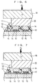
- the semiconductor device is mounted by carrying out a heating and pressurizing process applied in two stages whereby the adhesive resin 11 is cured after the provisional press-bonding is applied. Consequently, the following effect, differing from that for the conventional case, can be brought about. The effect is described hereinafter with reference to Figs. 6 and 7.
- Figs. 6 and 7 are enlarged schematic sectional views of a principal part of the steps shown in Figs. 3 and 4, respectively, for illustrating with clarity the state of the conductive particles 12 sandwiched between the respective bumps 14 and the respective wiring patterns 15.
- sufficient pressurizing is applied beforehand through the preceding step of provisional press-bonding as shown in Fig. 6 in mounting the semiconductor device 16 on the circuit board 17, unlike the conventional method whereby a pressurizing and heating and press-bonding process for curing the adhesive resin 11 of the anisotropic conductive adhesive 13 is carried out at a time.
- the conductive particles 12 have already been held sandwiched between the respective bumps 14 and the respective wiring patterns 15 (4 pieces thereof in the figure). Accordingly, even if heating for curing the adhesive resin 11 is applied subsequently, the conductive particles 12 remain sandwiched between the respective bumps 14 and the respective wiring patterns 15, and will not flow outside of the respective bumps 14 even if the adhesive resin 11 becomes fluidized. This makes it possible to arrest more of the conductive particles 12 between the respective bumps 14 and the respective wiring patterns 15 while keeping the same in contact with both the respective bumps 14 and the respective wiring patterns 15.
- Fig. 8 shows the number of the conductive particles existing between the respective bumps and the respective wiring patterns in the case of mounting a semiconductor device using the method of mounting the same according to the invention in comparison with that in the case of mounting a semiconductor device using the conventional method of mounting the same.
- the vertical axis represents the number of the conductive particles. The figure shows that in the case of mounting the semiconductor device using the method of mounting the same according to the invention, there exist 8 pieces on average of the conductive particles while with the conventional method of mounting the semiconductor device, there exist about 5.5 pieces on average of the conductive particles. It is thus shown that, with the method of mounting the semiconductor device according to the invention, a greater number of the conductive particles remain in a connecting region between the respective bumps and the respective wiring patterns.
- the semiconductor device was mounted on a glass board by the method of mounting the same according to the invention, and by the conventional method of mounting the same, respectively, so as to be able to observe the connecting region, and the number of the conductive particles remaining in the connecting region was measured in respective cases.
- the step of fully curing the adhesive resin 11 of the anisotropic conductive adhesive 13 is carried out by applying the heating and pressurizing process using the heating and pressurizing tool 18, however, as shown in Fig. 9, the step described above may be carried out by placing the circuit board 17 with the semiconductor device 16 provisionally press-bonded thereto in a furnace 20 set at a temperature causing the adhesive resin 11 to be cured, in the range of 150 to 250°C, and by subsequently supplying heat from a heat source 21 of the furnace 20.
- the step described above may be carried out by placing the circuit board 17 with the semiconductor device 16 provisionally press-bonded thereto on top of a hot plate 30 set at a temperature causing the adhesive resin 11 to be cured, in the range of 150 to 250°C, and by heating for a duration of about 5 to 30 seconds.
- the hot plate 30 is provided with a built-in heater 31.
- provisional press-bonding is applied at a temperature at which the adhesive resin has low fluidity, prior to curing of the anisotropic conductive adhesive, so that a large number of the conductive particles can be held sandwiched between the respective bumps and the respective wiring patterns.
- connection to finer wiring patterns becomes possible so as to be adaptable for high-density mounting.
Landscapes
- Engineering & Computer Science (AREA)
- Manufacturing & Machinery (AREA)
- Microelectronics & Electronic Packaging (AREA)
- Wire Bonding (AREA)
- Electric Connection Of Electric Components To Printed Circuits (AREA)
Abstract
Description
Claims (6)
- A method of mounting a semiconductor device using an anisotropic conductive adhesive, comprising;a step of disposing the anisotropic conductive adhesive, composed of conductive particles mixed in an adhesive resin of a thermosetting type, in a region on the surface of a circuit board, where wiring patterns are formed;a step of placing the semiconductor device on the surface of the circuit board after aligning bumps provided on the semiconductor device with the wiring patterns formed on the surface of the circuit board, respectively;a step of provisionally press-bonding the semiconductor device onto the circuit board by applying a predetermined pressure thereto at a temperature lower than the curing temperature of the adhesive resin of the anisotropic conductive adhesive; anda step of bonding the semiconductor device, as provisionally press-bonded, onto the circuit board by curing the adhesive resin at a temperature causing the adhesive resin to be cured.
- A method of mounting a semiconductor device using an anisotropic conductive adhesive according to claim 1, wherein electric conduction is effected between the bumps of the semiconductor device and the wiring patterns of the circuit board, respectively, in the step of provisionally press-bonding the semiconductor device onto the circuit board.
- A method of mounting a semiconductor device using an anisotropic conductive adhesive according to claim 1, wherein the step of bonding the semiconductor device, as provisionally press-bonded, onto the circuit board is performed by means of thermal press-bonding using a heating and pressurizing tool set at a temperature causing the adhesive resin to be cured.
- A method of mounting a semiconductor device using an anisotropic conductive adhesive according to claim 1 or 2, wherein the step of bonding the semiconductor device, as provisionally press-bonded, onto the circuit board is performed by placing the circuit board with the semiconductor device provisionally press-bonded thereto in a furnace set at a temperature causing the adhesive resin to be cured.
- A method of mounting a semiconductor device using an anisotropic conductive adhesive according to claim 1, wherein the step of bonding the semiconductor device as provisionally press-bonded, onto the circuit board is performed by placing the circuit board with the semiconductor device provisionally press-bonded thereto on a hot plate set at a temperature causing the adhesive resin to be cured.
- A method of mounting a semiconductor device using an anisotropic conductive adhesive according to claim 1, wherein the conductive particles are brought into contact with the bumps of the semiconductor device and the wiring patterns of the circuit board, respectively, in the step of provisionally press-bonding the semiconductor device onto the circuit board.
Applications Claiming Priority (3)
| Application Number | Priority Date | Filing Date | Title |
|---|---|---|---|
| JP1848799 | 1999-01-27 | ||
| JP1848799 | 1999-01-27 | ||
| PCT/JP2000/000420 WO2000045431A1 (en) | 1999-01-27 | 2000-01-27 | Method of packaging semiconductor device using anisotropic conductive adhesive |
Publications (3)
| Publication Number | Publication Date |
|---|---|
| EP1067598A1 true EP1067598A1 (en) | 2001-01-10 |
| EP1067598A4 EP1067598A4 (en) | 2001-10-24 |
| EP1067598B1 EP1067598B1 (en) | 2003-03-26 |
Family
ID=11973005
Family Applications (1)
| Application Number | Title | Priority Date | Filing Date |
|---|---|---|---|
| EP00901937A Expired - Lifetime EP1067598B1 (en) | 1999-01-27 | 2000-01-27 | Method of packaging semiconductor device using anisotropic conductive adhesive |
Country Status (7)
| Country | Link |
|---|---|
| US (1) | US6498051B1 (en) |
| EP (1) | EP1067598B1 (en) |
| KR (1) | KR100382759B1 (en) |
| CN (1) | CN1135611C (en) |
| BR (1) | BR0004470A (en) |
| DE (1) | DE60001776T2 (en) |
| WO (1) | WO2000045431A1 (en) |
Cited By (6)
| Publication number | Priority date | Publication date | Assignee | Title |
|---|---|---|---|---|
| EP1047124A3 (en) * | 1999-04-20 | 2001-11-07 | Sony Chemicals Corporation | Process for producing semiconductor device |
| FR2812223A1 (en) * | 2000-07-28 | 2002-02-01 | Thomson Csf | METHOD FOR BONDING ELECTRONIC CIRCUIT SUBSTRATES TO A SOLE AND DEVICE FOR IMPLEMENTING THE METHOD |
| DE10120928C1 (en) * | 2001-04-30 | 2002-10-31 | Infineon Technologies Ag | Production of contact joint between semiconductor chip and substrate comprises applying hardenable conducting adhesive on contact surfaces of substrate and chip, joining, and hardening adhesive to form contact joint |
| WO2012000114A1 (en) * | 2010-06-29 | 2012-01-05 | Cooledge Lightning Inc. | Electronic devices with yielding substrates |
| EP2479786A4 (en) * | 2009-09-18 | 2013-04-03 | Bondtech Co Ltd | PRESSING DEVICE AND PRESSING METHOD |
| US9765936B2 (en) | 2009-06-27 | 2017-09-19 | Cooledge Lighting Inc. | High efficiency LEDs and LED lamps |
Families Citing this family (33)
| Publication number | Priority date | Publication date | Assignee | Title |
|---|---|---|---|---|
| JP2003204142A (en) * | 2002-01-08 | 2003-07-18 | Sumitomo Metal Micro Devices Inc | Electronic component mounting method and electronic component mounting apparatus |
| JP3886401B2 (en) * | 2002-03-25 | 2007-02-28 | ソニーケミカル&インフォメーションデバイス株式会社 | Method for manufacturing connection structure |
| JP2004260135A (en) * | 2003-02-06 | 2004-09-16 | Sanyo Electric Co Ltd | Semiconductor integrated device and method of manufacturing the same |
| US20070075436A1 (en) * | 2003-10-06 | 2007-04-05 | Nec Corporation | Electronic device and manufacturing method of the same |
| JP3835556B2 (en) * | 2003-10-27 | 2006-10-18 | セイコーエプソン株式会社 | Semiconductor device manufacturing method and semiconductor device manufacturing apparatus |
| JP4432949B2 (en) * | 2006-09-15 | 2010-03-17 | パナソニック株式会社 | Electrical component connection method |
| CN101303443A (en) * | 2007-05-11 | 2008-11-12 | 鸿富锦精密工业(深圳)有限公司 | Camera module and assembly method thereof |
| JP5093482B2 (en) * | 2007-06-26 | 2012-12-12 | ソニーケミカル&インフォメーションデバイス株式会社 | Anisotropic conductive material, connection structure and manufacturing method thereof |
| JP5622137B2 (en) * | 2007-10-29 | 2014-11-12 | デクセリアルズ株式会社 | Electrical connection body and manufacturing method thereof |
| US9480133B2 (en) | 2010-01-04 | 2016-10-25 | Cooledge Lighting Inc. | Light-emitting element repair in array-based lighting devices |
| US8653539B2 (en) | 2010-01-04 | 2014-02-18 | Cooledge Lighting, Inc. | Failure mitigation in arrays of light-emitting devices |
| JP2012204588A (en) * | 2011-03-25 | 2012-10-22 | Disco Abrasive Syst Ltd | Semiconductor device chip mounting method |
| JP2012204589A (en) * | 2011-03-25 | 2012-10-22 | Disco Abrasive Syst Ltd | Semiconductor device wafer bonding method |
| US20130032270A1 (en) * | 2011-08-01 | 2013-02-07 | Texas Instruments Incorporated | Thermal compression bonding with separate bond heads |
| US20130056749A1 (en) * | 2011-09-07 | 2013-03-07 | Michael Tischler | Broad-area lighting systems |
| US20130187540A1 (en) | 2012-01-24 | 2013-07-25 | Michael A. Tischler | Discrete phosphor chips for light-emitting devices and related methods |
| US8907362B2 (en) | 2012-01-24 | 2014-12-09 | Cooledge Lighting Inc. | Light-emitting dies incorporating wavelength-conversion materials and related methods |
| US8896010B2 (en) | 2012-01-24 | 2014-11-25 | Cooledge Lighting Inc. | Wafer-level flip chip device packages and related methods |
| US8877561B2 (en) | 2012-06-07 | 2014-11-04 | Cooledge Lighting Inc. | Methods of fabricating wafer-level flip chip device packages |
| US20140069696A1 (en) * | 2012-09-11 | 2014-03-13 | Apple Inc. | Methods and apparatus for attaching multi-layer flex circuits to substrates |
| JP6163838B2 (en) * | 2013-04-05 | 2017-07-19 | 富士電機株式会社 | Pressure heating joining structure and pressure heating joining method |
| US9343443B2 (en) | 2014-02-05 | 2016-05-17 | Cooledge Lighting, Inc. | Light-emitting dies incorporating wavelength-conversion materials and related methods |
| DE102014104510B4 (en) * | 2014-03-31 | 2019-02-07 | Gottfried Wilhelm Leibniz Universität Hannover | Method for joining and device for joining an assembly using the method |
| US9720696B2 (en) | 2014-09-30 | 2017-08-01 | International Business Machines Corporation | Independent mapping of threads |
| US10133576B2 (en) | 2015-01-13 | 2018-11-20 | International Business Machines Corporation | Parallel slice processor having a recirculating load-store queue for fast deallocation of issue queue entries |
| JP6679370B2 (en) * | 2015-03-26 | 2020-04-15 | デクセリアルズ株式会社 | Flexible mounting module body manufacturing method |
| JP6715052B2 (en) * | 2016-03-25 | 2020-07-01 | デクセリアルズ株式会社 | Method for manufacturing connection structure |
| JP6935702B2 (en) * | 2016-10-24 | 2021-09-15 | デクセリアルズ株式会社 | Anisotropic conductive film |
| JP6826060B2 (en) * | 2017-03-30 | 2021-02-03 | 芝浦メカトロニクス株式会社 | Crimping device |
| US10420222B2 (en) * | 2017-04-20 | 2019-09-17 | Palo Alto Research Center Incorporated | Method for bonding discrete devices using anisotropic conductive film |
| US10795452B2 (en) * | 2018-02-07 | 2020-10-06 | Microsoft Technology Licensing, Llc | Multi-stage cure bare die light emitting diode |
| KR102707392B1 (en) * | 2019-04-29 | 2024-09-20 | 삼성전자주식회사 | Bonding head and a bonding apparatus having the same |
| CN114597138A (en) * | 2020-12-03 | 2022-06-07 | 群创光电股份有限公司 | Manufacturing method of semiconductor package |
Family Cites Families (9)
| Publication number | Priority date | Publication date | Assignee | Title |
|---|---|---|---|---|
| JPS6197837A (en) | 1984-10-18 | 1986-05-16 | Matsushita Electronics Corp | Semiconductor etching device |
| JPS6197837U (en) * | 1984-12-04 | 1986-06-23 | ||
| EP0641019A3 (en) * | 1993-08-27 | 1995-12-20 | Poly Flex Circuits Inc | Flexible mounting frame printed on a polymer. |
| TW340132B (en) | 1994-10-20 | 1998-09-11 | Ibm | Structure for use as an electrical interconnection means and process for preparing the same |
| JPH09219579A (en) * | 1996-02-13 | 1997-08-19 | Oki Electric Ind Co Ltd | Electronic component connection method and connection device |
| JP3842362B2 (en) * | 1996-02-28 | 2006-11-08 | 株式会社東芝 | Thermocompression bonding method and thermocompression bonding apparatus |
| JP3096965B2 (en) * | 1996-07-16 | 2000-10-10 | 日立テクノエンジニアリング株式会社 | Substrate heating method and substrate heating furnace |
| US5943558A (en) * | 1996-09-23 | 1999-08-24 | Communications Technology, Inc. | Method of making an assembly package having an air tight cavity and a product made by the method |
| JPH10289929A (en) * | 1997-04-14 | 1998-10-27 | Seiko Epson Corp | How to mount surface mount components |
-
2000
- 2000-01-27 EP EP00901937A patent/EP1067598B1/en not_active Expired - Lifetime
- 2000-01-27 BR BR0004470-9A patent/BR0004470A/en not_active IP Right Cessation
- 2000-01-27 DE DE60001776T patent/DE60001776T2/en not_active Expired - Lifetime
- 2000-01-27 CN CNB008000379A patent/CN1135611C/en not_active Expired - Fee Related
- 2000-01-27 KR KR10-2000-7010512A patent/KR100382759B1/en not_active Expired - Fee Related
- 2000-01-27 WO PCT/JP2000/000420 patent/WO2000045431A1/en not_active Ceased
- 2000-01-27 US US09/646,964 patent/US6498051B1/en not_active Expired - Lifetime
Cited By (16)
| Publication number | Priority date | Publication date | Assignee | Title |
|---|---|---|---|---|
| EP1047124A3 (en) * | 1999-04-20 | 2001-11-07 | Sony Chemicals Corporation | Process for producing semiconductor device |
| US6518095B1 (en) | 1999-04-20 | 2003-02-11 | Sony Chemicals Corp. | Process for producing semiconductor device |
| FR2812223A1 (en) * | 2000-07-28 | 2002-02-01 | Thomson Csf | METHOD FOR BONDING ELECTRONIC CIRCUIT SUBSTRATES TO A SOLE AND DEVICE FOR IMPLEMENTING THE METHOD |
| DE10120928C1 (en) * | 2001-04-30 | 2002-10-31 | Infineon Technologies Ag | Production of contact joint between semiconductor chip and substrate comprises applying hardenable conducting adhesive on contact surfaces of substrate and chip, joining, and hardening adhesive to form contact joint |
| US6861291B2 (en) | 2001-04-30 | 2005-03-01 | Infineon Technologies Ag | Method producing a contact connection between a semiconductor chip and a substrate and the contact connection |
| US9966414B2 (en) | 2009-06-27 | 2018-05-08 | Cooledge Lighting Inc. | High efficiency LEDs and LED lamps |
| US9765936B2 (en) | 2009-06-27 | 2017-09-19 | Cooledge Lighting Inc. | High efficiency LEDs and LED lamps |
| US10281091B2 (en) | 2009-06-27 | 2019-05-07 | Cooledge Lighting Inc. | High efficiency LEDs and LED lamps |
| US10910522B2 (en) | 2009-06-27 | 2021-02-02 | Cooledge Lighting Inc. | High efficiency LEDs and LED lamps |
| US11415272B2 (en) | 2009-06-27 | 2022-08-16 | Cooledge Lighting, Inc. | High efficiency LEDs and LED lamps |
| EP2479786A4 (en) * | 2009-09-18 | 2013-04-03 | Bondtech Co Ltd | PRESSING DEVICE AND PRESSING METHOD |
| US9243894B2 (en) | 2009-09-18 | 2016-01-26 | Bondtech Co., Ltd. | Pressure application apparatus and pressure application method |
| US9379082B2 (en) | 2009-09-18 | 2016-06-28 | Bondtech Co., Ltd. | Pressure application apparatus and pressure application method |
| US9252373B2 (en) | 2010-06-29 | 2016-02-02 | Cooledge Lighting, Inc. | Electronic devices with yielding substrates |
| US9426860B2 (en) | 2010-06-29 | 2016-08-23 | Cooledge Lighting, Inc. | Electronic devices with yielding substrates |
| WO2012000114A1 (en) * | 2010-06-29 | 2012-01-05 | Cooledge Lightning Inc. | Electronic devices with yielding substrates |
Also Published As
| Publication number | Publication date |
|---|---|
| KR20010034625A (en) | 2001-04-25 |
| CN1293823A (en) | 2001-05-02 |
| DE60001776T2 (en) | 2004-02-05 |
| KR100382759B1 (en) | 2003-05-09 |
| EP1067598A4 (en) | 2001-10-24 |
| WO2000045431A1 (en) | 2000-08-03 |
| BR0004470A (en) | 2000-12-19 |
| CN1135611C (en) | 2004-01-21 |
| US6498051B1 (en) | 2002-12-24 |
| DE60001776D1 (en) | 2003-04-30 |
| EP1067598B1 (en) | 2003-03-26 |
Similar Documents
| Publication | Publication Date | Title |
|---|---|---|
| US6498051B1 (en) | Method of packaging semiconductor device using anisotropic conductive adhesive | |
| EP1445995B1 (en) | Method of mounting an electronic component on a circuit board and system for carrying out the method | |
| CN101322233B (en) | Method of bonding between electrical devices using ultrasonic vibrations | |
| US5739053A (en) | Process for bonding a semiconductor to a circuit substrate including a solder bump transferring step | |
| JP4345598B2 (en) | Circuit board connection structure and manufacturing method thereof | |
| US7736950B2 (en) | Flip chip interconnection | |
| KR100288035B1 (en) | Flip chip connection method, flip chip connection structure and electronic device using same | |
| JP3326382B2 (en) | Method for manufacturing semiconductor device | |
| KR20030080035A (en) | Electric device producing method | |
| CN100411163C (en) | Semiconductor devices with chips on thin films | |
| EP0662256A1 (en) | An electrical connecting structure and a method for electrically connecting terminals to each other | |
| JP2002026070A (en) | Semiconductor device and method of manufacturing the same | |
| KR102535108B1 (en) | Bonding method using laser | |
| JPH1041694A (en) | Substrate mounting structure of semiconductor element and mounting method thereof | |
| US6132226A (en) | Structure and method for mounting an electronic part | |
| JP2001024032A (en) | IC chip mounting method and device for contactless IC card | |
| JP2000058597A (en) | Electronic component mounting method | |
| JP2003347359A (en) | Driver IC crimping apparatus and crimping method | |
| JP3267071B2 (en) | TAB-cell crimping apparatus and crimping method | |
| JPH0671026B2 (en) | Semiconductor mounting method | |
| JP2002016104A (en) | Semiconductor device mounting method and semiconductor device mounted body manufacturing method | |
| JP2001007488A (en) | Semiconductor device mounting structure and mounting method thereof | |
| JP2004363167A (en) | Wiring board interconnection method | |
| JP2003133371A (en) | Semiconductor device manufacturing method and manufacturing apparatus | |
| JP2004031865A (en) | Connection method between liquid crystal display panel and drive circuit |
Legal Events
| Date | Code | Title | Description |
|---|---|---|---|
| PUAI | Public reference made under article 153(3) epc to a published international application that has entered the european phase |
Free format text: ORIGINAL CODE: 0009012 |
|
| 17P | Request for examination filed |
Effective date: 20000908 |
|
| AK | Designated contracting states |
Kind code of ref document: A1 Designated state(s): CH DE FR GB LI NL |
|
| A4 | Supplementary search report drawn up and despatched |
Effective date: 20010912 |
|
| AK | Designated contracting states |
Kind code of ref document: A4 Designated state(s): CH DE FR GB LI NL |
|
| RAP1 | Party data changed (applicant data changed or rights of an application transferred) |
Owner name: CITIZEN WATCH CO. LTD. |
|
| 17Q | First examination report despatched |
Effective date: 20020225 |
|
| GRAH | Despatch of communication of intention to grant a patent |
Free format text: ORIGINAL CODE: EPIDOS IGRA |
|
| GRAH | Despatch of communication of intention to grant a patent |
Free format text: ORIGINAL CODE: EPIDOS IGRA |
|
| GRAA | (expected) grant |
Free format text: ORIGINAL CODE: 0009210 |
|
| AK | Designated contracting states |
Designated state(s): CH DE FR GB LI NL |
|
| PG25 | Lapsed in a contracting state [announced via postgrant information from national office to epo] |
Ref country code: CH Free format text: LAPSE BECAUSE OF FAILURE TO SUBMIT A TRANSLATION OF THE DESCRIPTION OR TO PAY THE FEE WITHIN THE PRESCRIBED TIME-LIMIT Effective date: 20030326 Ref country code: NL Free format text: LAPSE BECAUSE OF FAILURE TO SUBMIT A TRANSLATION OF THE DESCRIPTION OR TO PAY THE FEE WITHIN THE PRESCRIBED TIME-LIMIT Effective date: 20030326 Ref country code: LI Free format text: LAPSE BECAUSE OF FAILURE TO SUBMIT A TRANSLATION OF THE DESCRIPTION OR TO PAY THE FEE WITHIN THE PRESCRIBED TIME-LIMIT Effective date: 20030326 |
|
| REG | Reference to a national code |
Ref country code: GB Ref legal event code: FG4D |
|
| REG | Reference to a national code |
Ref country code: CH Ref legal event code: EP |
|
| REF | Corresponds to: |
Ref document number: 60001776 Country of ref document: DE Date of ref document: 20030430 Kind code of ref document: P |
|
| NLV1 | Nl: lapsed or annulled due to failure to fulfill the requirements of art. 29p and 29m of the patents act | ||
| ET | Fr: translation filed | ||
| REG | Reference to a national code |
Ref country code: CH Ref legal event code: PL |
|
| PLBE | No opposition filed within time limit |
Free format text: ORIGINAL CODE: 0009261 |
|
| STAA | Information on the status of an ep patent application or granted ep patent |
Free format text: STATUS: NO OPPOSITION FILED WITHIN TIME LIMIT |
|
| 26N | No opposition filed |
Effective date: 20031230 |
|
| REG | Reference to a national code |
Ref country code: FR Ref legal event code: CD |
|
| PGFP | Annual fee paid to national office [announced via postgrant information from national office to epo] |
Ref country code: GB Payment date: 20100202 Year of fee payment: 11 |
|
| PGFP | Annual fee paid to national office [announced via postgrant information from national office to epo] |
Ref country code: DE Payment date: 20110119 Year of fee payment: 12 Ref country code: FR Payment date: 20110128 Year of fee payment: 12 |
|
| GBPC | Gb: european patent ceased through non-payment of renewal fee |
Effective date: 20110127 |
|
| PG25 | Lapsed in a contracting state [announced via postgrant information from national office to epo] |
Ref country code: GB Free format text: LAPSE BECAUSE OF NON-PAYMENT OF DUE FEES Effective date: 20110127 |
|
| REG | Reference to a national code |
Ref country code: FR Ref legal event code: ST Effective date: 20120928 |
|
| PG25 | Lapsed in a contracting state [announced via postgrant information from national office to epo] |
Ref country code: DE Free format text: LAPSE BECAUSE OF NON-PAYMENT OF DUE FEES Effective date: 20120801 |
|
| REG | Reference to a national code |
Ref country code: DE Ref legal event code: R119 Ref document number: 60001776 Country of ref document: DE Effective date: 20120801 |
|
| PG25 | Lapsed in a contracting state [announced via postgrant information from national office to epo] |
Ref country code: FR Free format text: LAPSE BECAUSE OF NON-PAYMENT OF DUE FEES Effective date: 20120131 |