EP1067584A2 - Verbesserte Kühlung einer Spule für IMP-Prozess - Google Patents
Verbesserte Kühlung einer Spule für IMP-Prozess Download PDFInfo
- Publication number
- EP1067584A2 EP1067584A2 EP00114546A EP00114546A EP1067584A2 EP 1067584 A2 EP1067584 A2 EP 1067584A2 EP 00114546 A EP00114546 A EP 00114546A EP 00114546 A EP00114546 A EP 00114546A EP 1067584 A2 EP1067584 A2 EP 1067584A2
- Authority
- EP
- European Patent Office
- Prior art keywords
- support
- chamber
- coil
- electrically conductive
- conductive member
- Prior art date
- Legal status (The legal status is an assumption and is not a legal conclusion. Google has not performed a legal analysis and makes no representation as to the accuracy of the status listed.)
- Withdrawn
Links
Images


Classifications
-
- H—ELECTRICITY
- H10—SEMICONDUCTOR DEVICES; ELECTRIC SOLID-STATE DEVICES NOT OTHERWISE PROVIDED FOR
- H10P—GENERIC PROCESSES OR APPARATUS FOR THE MANUFACTURE OR TREATMENT OF DEVICES COVERED BY CLASS H10
- H10P95/00—Generic processes or apparatus for manufacture or treatments not covered by the other groups of this subclass
-
- H—ELECTRICITY
- H10—SEMICONDUCTOR DEVICES; ELECTRIC SOLID-STATE DEVICES NOT OTHERWISE PROVIDED FOR
- H10P—GENERIC PROCESSES OR APPARATUS FOR THE MANUFACTURE OR TREATMENT OF DEVICES COVERED BY CLASS H10
- H10P72/00—Handling or holding of wafers, substrates or devices during manufacture or treatment thereof
- H10P72/04—Apparatus for manufacture or treatment
- H10P72/0431—Apparatus for thermal treatment
- H10P72/0432—Apparatus for thermal treatment mainly by conduction
Definitions
- the present invention relates to a system and method for processing substrates.
- Sub-quarter micron multi-level metallization represents one of the key technologies for the next generation of ultra large scale integration (ULSI) for integrated circuits (ICs).
- ULSI ultra large scale integration
- ICs integrated circuits
- ULSI ultra large scale integration
- the widths of vias, contacts and other features decrease to 0.2 ⁇ m or less, while the thicknesses of the dielectric layers remains substantially constant, with the result that the aspect ratios for the features , i.e., their height divided by width, increases.
- Many traditional deposition processes have difficulty filling structures where the aspect ratio exceeds 4:1, and particularly where it approaches 10:1.
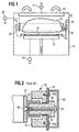
- FIG. 1 is a schematic of a typical IMP chamber 10, having a coil 22 supported by a support 30 in the chamber 10.
- processing gas such as helium or argon
- a power supply 12 delivers a bias to a target 14 to generate a plasma 13 of processing gas ions between the target and a substrate support 16, that supports a substrate 18.
- the ions impact the target and sputter material from the target, where some of the material is directed toward the substrate.
- a second power supply 20 delivers power to a coil 22 that is disposed between the target 14 and the substrate 18.
- the coil increases the density of the plasma and ionizes the sputtered material that traverses through the magnetic fields generated by the coil and the intensified plasma.
- a third power supply 24 biases the substrate and attracts the sputtered material ions in a highly directionalized manner to the surface of the substrate to better fill high aspect ratio features in the substrate.
- a clamp ring 26 is circumferentially disposed about the substrate to retain the substrate in position.
- a shield 28 is disposed between the chamber sidewalls and the sputtered material to avoid deposition of the sputtered material on the chamber sidewalls. Because the shield 28 is conductive, typically made of aluminum, and grounded and the coil 22 is conductive and electrically powered, electrical insulation between the two components is typically desired with an electrically insulative support 30.
- FIG. 2 shows details of the typical support 30 of Figure 1.
- the coil 22 is attached to the shield 28 by the combination of an internally threaded pin 36 at the coil coupled with a screw 34 near the shield having external threads 32. Because the coil is also sputtered by the plasma ions during the process, the coil is generally made from the same material as the target, e.g., copper.
- the pin and screw are insulated from the shield by an insulative support labyrinth 40, typically made of aluminum oxide (alumina).
- the alumina labyrinth is both electrically and thermally insulative.
- An inner cup 42 is placed between the coil and the support labyrinth to protect the inner surfaces of the support 30 from the sputtered material in proximity to the support.
- the inner cup is also made from the same material as the coil.
- An outer cup 44 attached to the shield by bolts 46a, 46b, circumferentially encloses a portion of the inner cup to reduce sputtered material deposition on the inner surfaces of the support 30 and is generally made of conductive material, such as stainless steel.
- the assembly of the inner cup, support labyrinth, and outer cup between the shield and the coil are held in position by the screw 34 and pin 36.
- An insulative ceramic cap 48 protects and insulates the screw 34 from the chamber surfaces.
- heat buildup in the chamber can have disadvantageous effects on the substrate process and resulting films.
- the heat can cause the structural components, such as the coil, to be distorted in shape, thereby altering the plasma density and shape.
- An increase in temperature can also cause the sputtering rates to change with varying coil temperatures.
- Increased temperatures can also limit the amount of power which can be applied to the coil without causing overheating of the coil.
- heat can be dissipated through conductive elements attached to a heat sink.
- typical conductive materials that channel heat to a heat sink are also electrically conductive which would disadvantageously affect the ability of the coil or other insulated electrical components to function properly.
- the heat dissipation is hindered under vacuum conditions by the typical attachment, such as bolting or clamping, of the structural components.
- the typical attachment such as bolting or clamping
- Even polished surfaces under magnification show irregularities in the surface.
- the heat transfer across the interface between the surfaces is limited to the direct contact of the microscopic surfaces and hindered by the absence of interspaced molecules under vacuum conditions between the non-contacting portions of the two surfaces.
- greater numbers of interfaces causes an increased resistance to conduction.
- the typical support 30 has several interfaces and thus interferes with heat transfer.
- the present invention generally provides a substrate processing system having a thermally conductive and electrically insulative member coupled to a heated member that provides for heat dissipation from the heated member.
- the invention relates to a system and method having a thermally conductive and electrically insulative member to dissipate heat in a substrate processing chamber.
- the present invention provides for heat dissipation through thermal conductance of an electrically insulated coil in an IMP reaction chamber.
- the invention provides a system for processing a substrate, comprising a chamber, an electrically conductive member, and a thermally conductive and electrically insulative support supporting the electrically conductive member comprising a component having a thermal conductance value of at least 90 watts per meter-degree Kelvin (W/m-K) and an dielectric strength value as an indicator of electrical resistivity of at least 10 14 kilovolts/millimeter (kV/mm).
- W/m-K watts per meter-degree Kelvin
- kV/mm dielectric strength value
- the invention provides a system for processing a substrate, comprising a chamber, an electrically conductive member in proximity to the chamber, and a thermally conductive and electrically insulative support supporting the electrically conductive member, the support comprising a component selected from the group consisting essentially of aluminum nitride and beryllium oxide.
- the invention provides a support for a substrate processing system comprising a ceramic and a metal conductor bonded to the ceramic.
- the invention also includes a method of cooling a substrate processing chamber, comprising providing a chamber, supporting an electrically conductive member in the chamber with a thermally conductive and electrically insulative bonded support, and providing at least one heat flow path from the electrically conductive member to the chamber through one or more bonded connections of the support.
- the invention provides a support for a substrate processing system, comprising a semi-conductor ceramic having a thermal conductance value of at least 90 W/m-K and a dielectric strength value of at least 10 14 kV/mm.
- the invention provides a support for a substrate processing system, comprising a semi-conductor ceramic selected from the group consisting essentially of aluminum nitride and beryllium oxide.
- FIG 3 is a schematic cross-sectional view of an IMP chamber 100 in which the support of the present invention may be used to advantage to electrically insulate an electrically conductive member, such as a coil from other camber components.
- An ion metal plasma (IMP) processing chamber known as an IMP VECTRATM chamber is available from Applied Material Inc. of Santa Clara, California.
- the IMP chamber can be integrated into an Endura® platform, also available from Applied Materials, Inc.
- the chamber 100 includes sidewalls 101, lid 102, and bottom 103.
- the lid 102 includes a target backing plate 104 which supports a target 105 of the material to be deposited.
- An opening 108 in the chamber 100 provides access for a robot (not shown) to deliver and retrieve substrates 110 to and from the chamber.
- a substrate support 112 supports the substrate 110 and is typically grounded.
- the substrate support is mounted on a lift motor 114 that raises and lowers the substrate support 112 and a substrate 110 disposed thereon.
- a lift plate 116 connected to a lift motor 118 is mounted in the chamber and raises and lowers pins 120a, 120b mounted in the substrate support. The pins raise and lower the substrate 110 from and to the surface of the substrate support 112.
- a coil 122 is mounted between the substrate support 112 and the target 105 and provides inductive magnetic fields in the chamber to assist in generating and maintaining a plasma between the target and substrate. The coil densifies the plasma which ionizes the sputtered material. The ionized material is then directed toward the substrate and deposited thereon.
- a shield 124 is disposed in the chamber to shield the chamber walls from the sputtered material.
- the shield also supports the coil 122 via supports 50 of the invention.
- the supports 50 electrically insulate the coil 122 from the shield 124 and the chamber 100.
- the clamp ring 128 is mounted between the coil 122 and the substrate support 112 and shields an outer edge and backside of the substrate from sputtered materials when the substrate is raised into a processing position to engage the lower portion of the clamp ring.
- the shield 124 supports the clamp ring when the substrate is lowered below the shield to enable substrate transfer.
- a power supply 130 delivers either RF or DC power to capacitively couple energy into target 105 to cause the processing gas to form a plasma.
- Magnets 106a, 106b disposed behind the target plate 104 increase the density of a plasma adjacent to the target in order to increase the sputtering efficiency.
- a power source 132 preferably a RF power source, supplies electrical power in the megahertz range to the coil 122 to increase the density of the plasma.
- Another power source 134 biases the substrate support 112 with respect to the plasma and provides directional attraction of the ionized sputtered material toward the substrate.
- Processing gas such as an inert gas of argon or helium
- gas inlet 136 from gas sources 138, 140 as metered by respective mass flow controllers 142, 144.
- a vacuum pump 146 is connected to the chamber at an exhaust port 148 to exhaust the chamber and maintain the desired pressure in the chamber.
- a controller 149 controls the functions of the power supplies, lift motors, mass flow controllers for gas injection, vacuum pump, and other associated chamber components and functions.
- the controller 149 preferably comprises a programmable microprocessor and executes system control software stored in a memory, which in the preferred embodiment is a hard disk drive, and can include analog and digital input/output boards, interface boards, and stepper motor controller boards (not shown).
- the controller 149 controls electrical power to the components of the chamber and includes a panel that allows an operator to monitor and operate the chamber.
- Optical and/or magnetic sensors are generally used to move and determine the position of movable mechanical assemblies.
- a support 50 of the invention provides electrical insulation for the coil 122 and yet also provides thermal conductance from the coil 122 for the heat generated in the substrate processing chamber 100.
- the material selection can be a combination of electrical insulation capabilities coupled with thermal conductance capabilities.
- FIG. 4 is a schematic view in partial cross section of a electrically insulating and thermally conducting support 50 according to the invention that supports an electrically conductive member, e.g., a coil 52.
- the coil 52 is attached to a shield 28 by an internally threaded pin 54 coupled with a screw 56 having threads 57.
- the coil is made from the same material as the target, for instance, copper.
- An inner cup 58 is disposed between the coil and an inner conductor 60 to protect the inner surfaces of the support 50 from the plasma. Because the inner cup is exposed to the plasma ions, generally the inner cup is also made from the same material as the coil.
- the inner conductor 60 can be conductive and can also be made of the same material as the coil 52 and the inner cup 58 and assists in transferring the heat from the coil 52.
- a dielectric element 62 is disposed between the inner conductor 60 and toward the shield 28.
- the dielectric element 62 is preferably an electrically insulative and thermally conductive material.
- One preferred material is aluminum nitride.
- Another material could be beryllium oxide. Both materials exhibit a thermal conductance value of at least 90 watts per meter-degree Kelvin (W/m-K) and a dielectric strength value as an indicator of electrical resistivity of at least 10 14 kilovolts/millimeter (kV/mm).
- W/m-K watts per meter-degree Kelvin
- kV/mm dielectric strength value
- Other materials having the electrical and thermal characteristics named herein would also be suitable.
- Disposed outward from the dielectric element 62 is an outer conductor 64 which is engaged against the shield 28 and can transmit thermal energy thereto.
- the outer conductor 64 can be made of conductive material, such as copper, and can be the same material as the inner conductor 60.
- the two conductors 60, 64 and the thermally conductive dielectric element 62 transfer thermal energy between the coil 52 and the shield 28, while the dielectric element 62 provides electrical insulation between the coil 52 and the shield 28.
- the thermal conductance is further enhanced by bonding at least one of the conductors 60, 64 with the dielectric element 62.
- the present invention increases the thermal conductance by bonding at least one of the conductors 60, 64 with the dielectric element 62. Bonding can be achieved by brazing, soldering, or other methods known to bond two components together.
- Bonding lessens the interface effects experienced due to vacuum conditions and physical clamping type connections.
- the outer conductor 64 and dielectric element 62 are brazed together at joint 63.
- the inner conductor 60 is not shown bonded to the dielectric element 62, although in some embodiments, such connection could further enhance the thermal conductance.
- the inner cup 58 could be bonded to the coil 52 and the outer conductor 64 could be bonded to the shield 28 in some embodiments.
- the lack of bonding of the outer conductor 64 to the dielectric element 62 reflects practical considerations of assembly and maintenance.
- An outer cup 66 attached to the shield 28 by threaded connectors 68, 70, circumferentially encloses a portion of the inner cup 58 to reduce sputtered material deposition on the inner surfaces of the support 50 and is generally made of conductive material, such as stainless steel.
- a screw head of the screw 56 engages a clamp 72 to assist in pressing the various elements together between the screw 56 at the shield 28 and the pin 54 at the coil 52. If the clamp 72 is conductive, then it may be desirable to insulate the clamp 72 from the shield 28 by a clamp insulator 74, disposed between the clamp 72 and the shield 28. If the screw 56 is non-conductive, then such insulation may be unnecessary.
- the clamp 72 is electrically conductive and extends through the shield 28 and is electrically insulated from the shield 28 by a liner 76. If the clamp 72 is non-conductive, then such electrical insulation may also be unnecessary.
- An insulative ceramic cap 78 made of insulative material such as alumina, protects and insulates the screw 56 and/or other conductive elements from the chamber surfaces.
- FIG 5 is a schematic cross sectional view of an alternative embodiment of the support 50.
- the coil 82 includes the inner conductor 60 and inner cup 58, shown in Figure 4, and thus provides a continuous thermal transfer through those components without any interfaces.
- a dielectric element 86 is disposed between the coil 82 and the shield 28.
- the dielectric element 86 can be made of the same material as the dielectric element 62 shown in Figure 4.
- the coil 82 and dielectric element 86 are coupled to the shield 28 by a threaded screw 83 which passes through a ceramic washer 80, through the dielectric element 86, and into a threaded hole 84 in the coil 82.
- the support 50 is protected on the shield 28 by the ceramic cap 78. This embodiment of the support 50 reduces the number of interfaces between the coil and the shield.
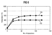
- FIG 6 shows test results obtained by comparing temperatures of a typical coil 122 shown in Figure 3 using a prior art support 30 and a support 50 of the present invention.
- Each support was mounted in a chamber, coupled to the coil 122, and the processing initiated.
- the transient coil temperature was incrementally measured over a number of deposition cycles.
- the process regime used for these tests was as follows. About 2000 watts (W) of DC power was delivered to the target to generate the plasma. About 2000 W of RF power was delivered to the coil 122 to densify the plasma arid ionize the sputtered target material traversing the plasma.
- the duty cycle was about 50%, that is, the time the coil was powered was about equal to the time the coil was not powered.
- About 350 W of DC power was delivered to the substrate support 112 to bias the substrate 110 and attract the ionized sputtered material to the substrate 110.
- a chamber pressure was maintained at about 20 mTorr.
- An upper line 150 shown in Figure 5 represents the coil temperature of the prior art support 30.
- the coil temperature increased to about 600°C after about 80 deposition cycles.
- the lower line 154 represents the coil temperature of the support 50 of the present invention.
- the lower line 154 shows that the coil temperature increased to a temperature of about 400°C after only about 40 deposition cycles and maintained this temperature for about 125 deposition cycles.
- the support 50 of the present invention provided a lower coil temperature and stabilized faster than a typical prior art support 30.
- the lower coil temperature adds stability to the substrate processing due to a smaller change in temperature of the coil from process initiation and results in less coil and plasma distortion.
- Other test results also show that the temperature of the shield 124 is raised slightly, about 50°C, to a temperature of about 200°C, which indicates that the support 50 is indeed conducting more heat to the shield 124 and away from the coil 122.
Landscapes
- Plasma Technology (AREA)
- Physical Vapour Deposition (AREA)
- Physical Deposition Of Substances That Are Components Of Semiconductor Devices (AREA)
Applications Claiming Priority (2)
| Application Number | Priority Date | Filing Date | Title |
|---|---|---|---|
| US09/350,619 US6376807B1 (en) | 1999-07-09 | 1999-07-09 | Enhanced cooling IMP coil support |
| US350619 | 1999-07-09 |
Publications (1)
| Publication Number | Publication Date |
|---|---|
| EP1067584A2 true EP1067584A2 (de) | 2001-01-10 |
Family
ID=23377503
Family Applications (1)
| Application Number | Title | Priority Date | Filing Date |
|---|---|---|---|
| EP00114546A Withdrawn EP1067584A2 (de) | 1999-07-09 | 2000-07-06 | Verbesserte Kühlung einer Spule für IMP-Prozess |
Country Status (6)
| Country | Link |
|---|---|
| US (2) | US6376807B1 (de) |
| EP (1) | EP1067584A2 (de) |
| JP (1) | JP4672835B2 (de) |
| KR (1) | KR20010015243A (de) |
| SG (1) | SG114465A1 (de) |
| TW (1) | TW497117B (de) |
Cited By (2)
| Publication number | Priority date | Publication date | Assignee | Title |
|---|---|---|---|---|
| WO2006004673A1 (en) * | 2004-06-28 | 2006-01-12 | Honeywell International Inc. | Single piece coil support assemblies, coil constructions and methods of assembling coil constructions |
| CN102437003A (zh) * | 2011-12-07 | 2012-05-02 | 宁波江丰电子材料有限公司 | 聚焦环组合、imp溅射设备 |
Families Citing this family (19)
| Publication number | Priority date | Publication date | Assignee | Title |
|---|---|---|---|---|
| US6376807B1 (en) * | 1999-07-09 | 2002-04-23 | Applied Materials, Inc. | Enhanced cooling IMP coil support |
| TW503442B (en) * | 2000-02-29 | 2002-09-21 | Applied Materials Inc | Coil and coil support for generating a plasma |
| DE10124530B8 (de) * | 2001-05-19 | 2006-01-12 | Eads Deutschland Gmbh | Sensorstruktur zur Strömungsdatenmessung an einem Strömungskörper |
| US7067439B2 (en) | 2002-06-14 | 2006-06-27 | Applied Materials, Inc. | ALD metal oxide deposition process using direct oxidation |
| JP2006519315A (ja) * | 2003-02-28 | 2006-08-24 | ハネウェル・インターナショナル・インコーポレーテッド | 物理蒸着チャンバで使用するように形成されたコイル構造及びコイル構造の形成方法 |
| US20050098427A1 (en) * | 2003-11-11 | 2005-05-12 | Taiwan Semiconductor Manufacturing Co., Ltd. | RF coil design for improved film uniformity of an ion metal plasma source |
| JP4393897B2 (ja) * | 2004-03-12 | 2010-01-06 | 新明和工業株式会社 | 成膜装置 |
| US8119210B2 (en) | 2004-05-21 | 2012-02-21 | Applied Materials, Inc. | Formation of a silicon oxynitride layer on a high-k dielectric material |
| US20060105114A1 (en) * | 2004-11-16 | 2006-05-18 | White John M | Multi-layer high quality gate dielectric for low-temperature poly-silicon TFTs |
| US7837838B2 (en) * | 2006-03-09 | 2010-11-23 | Applied Materials, Inc. | Method of fabricating a high dielectric constant transistor gate using a low energy plasma apparatus |
| US7645710B2 (en) * | 2006-03-09 | 2010-01-12 | Applied Materials, Inc. | Method and apparatus for fabricating a high dielectric constant transistor gate using a low energy plasma system |
| US7678710B2 (en) | 2006-03-09 | 2010-03-16 | Applied Materials, Inc. | Method and apparatus for fabricating a high dielectric constant transistor gate using a low energy plasma system |
| TWI435376B (zh) * | 2006-09-26 | 2014-04-21 | 應用材料股份有限公司 | 用於缺陷鈍化之高k閘極堆疊的氟電漿處理 |
| US20090095714A1 (en) * | 2007-10-12 | 2009-04-16 | Tokyo Electron Limited | Method and system for low pressure plasma processing |
| US9371578B2 (en) | 2010-03-29 | 2016-06-21 | Jx Nippon Mining & Metals Corporation | Tantalum coil for sputtering and method for processing the coil |
| CA2819361C (en) | 2010-12-01 | 2018-06-12 | Parker-Hannifin Corporation | Bearing isolator seal |
| CN103602954B (zh) * | 2013-11-06 | 2016-02-24 | 深圳市华星光电技术有限公司 | 用于磁控溅射阳极棒的支撑件及包括其的磁控溅射装置 |
| US20150122643A1 (en) * | 2013-11-06 | 2015-05-07 | Shenzhen China Star Optoelectronics Technology Co., Ltd. | Supporting member for magnetron sputtering anode bar and magnetron sputtering device including the same |
| CN105436687A (zh) * | 2014-08-27 | 2016-03-30 | 宁波江丰电子材料股份有限公司 | 聚焦环组件的焊接方法 |
Family Cites Families (11)
| Publication number | Priority date | Publication date | Assignee | Title |
|---|---|---|---|---|
| US5078851A (en) * | 1989-07-26 | 1992-01-07 | Kouji Nishihata | Low-temperature plasma processor |
| DE69432383D1 (de) * | 1993-05-27 | 2003-05-08 | Applied Materials Inc | Verbesserungen betreffend Substrathalter geeignet für den Gebrauch in Vorrichtungen für die chemische Abscheidung aus der Dampfphase |
| JPH08227933A (ja) * | 1995-02-20 | 1996-09-03 | Shin Etsu Chem Co Ltd | 静電吸着機能を有するウエハ加熱装置 |
| US5677253A (en) * | 1995-03-30 | 1997-10-14 | Kyocera Corporation | Wafer holding member |
| JPH0978237A (ja) * | 1995-09-14 | 1997-03-25 | Nippon Dennetsu Co Ltd | 薄膜製造方法及びその装置 |
| JPH09213781A (ja) * | 1996-02-01 | 1997-08-15 | Tokyo Electron Ltd | 載置台構造及びそれを用いた処理装置 |
| JPH09260474A (ja) * | 1996-03-22 | 1997-10-03 | Sony Corp | 静電チャックおよびウエハステージ |
| FR2759243B1 (fr) * | 1997-02-03 | 1999-04-30 | Ferraz | Echangeur de chaleur pour composants electroniques et appareillages electrotechniques |
| JP3398300B2 (ja) * | 1997-05-28 | 2003-04-21 | 京セラ株式会社 | 電子装置 |
| JP3318514B2 (ja) * | 1997-08-06 | 2002-08-26 | 日本碍子株式会社 | 半導体支持装置 |
| US6376807B1 (en) * | 1999-07-09 | 2002-04-23 | Applied Materials, Inc. | Enhanced cooling IMP coil support |
-
1999
- 1999-07-09 US US09/350,619 patent/US6376807B1/en not_active Expired - Lifetime
-
2000
- 2000-07-04 SG SG200003698A patent/SG114465A1/en unknown
- 2000-07-06 EP EP00114546A patent/EP1067584A2/de not_active Withdrawn
- 2000-07-07 TW TW089113627A patent/TW497117B/zh not_active IP Right Cessation
- 2000-07-08 KR KR1020000039066A patent/KR20010015243A/ko not_active Ceased
- 2000-07-10 JP JP2000208308A patent/JP4672835B2/ja not_active Expired - Lifetime
-
2001
- 2001-12-10 US US10/016,350 patent/US6580057B2/en not_active Expired - Lifetime
Cited By (4)
| Publication number | Priority date | Publication date | Assignee | Title |
|---|---|---|---|---|
| WO2006004673A1 (en) * | 2004-06-28 | 2006-01-12 | Honeywell International Inc. | Single piece coil support assemblies, coil constructions and methods of assembling coil constructions |
| US7374648B2 (en) | 2004-06-28 | 2008-05-20 | Honeywell International Inc. | Single piece coil support assemblies, coil constructions and methods of assembling coil constructions |
| CN102437003A (zh) * | 2011-12-07 | 2012-05-02 | 宁波江丰电子材料有限公司 | 聚焦环组合、imp溅射设备 |
| CN102437003B (zh) * | 2011-12-07 | 2015-01-21 | 宁波江丰电子材料股份有限公司 | 聚焦环组合、imp溅射设备 |
Also Published As
| Publication number | Publication date |
|---|---|
| US20020046990A1 (en) | 2002-04-25 |
| JP4672835B2 (ja) | 2011-04-20 |
| US6376807B1 (en) | 2002-04-23 |
| JP2001098375A (ja) | 2001-04-10 |
| US6580057B2 (en) | 2003-06-17 |
| TW497117B (en) | 2002-08-01 |
| SG114465A1 (en) | 2005-09-28 |
| KR20010015243A (ko) | 2001-02-26 |
Similar Documents
| Publication | Publication Date | Title |
|---|---|---|
| US6376807B1 (en) | Enhanced cooling IMP coil support | |
| JP4256482B2 (ja) | 高温の静電チャックから下側の低温体に伝熱するための装置及び方法 | |
| KR101892911B1 (ko) | 정전 척 및 정전 척의 사용 방법들 | |
| EP1243016B1 (de) | Verfahren und vorrichtung zur physikalischen dampfabscheidung mittels ionen | |
| US5079481A (en) | Plasma-assisted processing magneton with magnetic field adjustment | |
| KR100458424B1 (ko) | 플라즈마 처리장치 | |
| WO1999057753A1 (en) | Apparatus for improved biasing and retaining of a workpiece in a workpiece processing system | |
| US5886864A (en) | Substrate support member for uniform heating of a substrate | |
| US9111968B2 (en) | Plasma processing chamber with a grounded electrode assembly | |
| KR102092623B1 (ko) | 플라스마 처리 장치 | |
| EP0790641A1 (de) | Kühlvorrichtung für ein Wafer | |
| KR20010030504A (ko) | 스퍼터된 도핑 씨드 층을 형성하는 방법 및 장치 | |
| WO2009005921A2 (en) | Polyceramic e-chuck | |
| WO2000019492A2 (en) | Cathode assembly containing an electrostatic chuck for retaining a wafer in a semiconductor wafer processing system | |
| KR20030051765A (ko) | 기판내의 고 애스펙트 비 형성체의 에칭 | |
| EP0983608A2 (de) | Aluminium abscheidungsabschirmung | |
| JPH06244143A (ja) | 処理装置 | |
| JPH07183277A (ja) | 処理装置 | |
| US20240387224A1 (en) | Electrostatic chucks with hybrid pucks to improve thermal performance and leakage current stability | |
| US12125734B2 (en) | Vacuum seal for electrostatic chuck | |
| JPH11209874A (ja) | スパッタリング装置及びターゲット | |
| JPH118208A (ja) | スパッタ装置 |
Legal Events
| Date | Code | Title | Description |
|---|---|---|---|
| PUAI | Public reference made under article 153(3) epc to a published international application that has entered the european phase |
Free format text: ORIGINAL CODE: 0009012 |
|
| AK | Designated contracting states |
Kind code of ref document: A2 Designated state(s): AT BE CH CY DE DK ES FI FR GB GR IE IT LI LU MC NL PT SE |
|
| AX | Request for extension of the european patent |
Free format text: AL;LT;LV;MK;RO;SI |
|
| STAA | Information on the status of an ep patent application or granted ep patent |
Free format text: STATUS: THE APPLICATION IS DEEMED TO BE WITHDRAWN |
|
| 18D | Application deemed to be withdrawn |
Effective date: 20040203 |