EP1066677B1 - Elektronische schaltungen - Google Patents
Elektronische schaltungen Download PDFInfo
- Publication number
- EP1066677B1 EP1066677B1 EP99938020A EP99938020A EP1066677B1 EP 1066677 B1 EP1066677 B1 EP 1066677B1 EP 99938020 A EP99938020 A EP 99938020A EP 99938020 A EP99938020 A EP 99938020A EP 1066677 B1 EP1066677 B1 EP 1066677B1
- Authority
- EP
- European Patent Office
- Prior art keywords
- signal
- function
- generating
- circuit
- carrier
- Prior art date
- Legal status (The legal status is an assumption and is not a legal conclusion. Google has not performed a legal analysis and makes no representation as to the accuracy of the status listed.)
- Expired - Lifetime
Links
Images


Classifications
-
- H—ELECTRICITY
- H03—ELECTRONIC CIRCUITRY
- H03D—DEMODULATION OR TRANSFERENCE OF MODULATION FROM ONE CARRIER TO ANOTHER
- H03D3/00—Demodulation of angle-, frequency- or phase- modulated oscillations
- H03D3/001—Details of arrangements applicable to more than one type of frequency demodulator
- H03D3/002—Modifications of demodulators to reduce interference by undesired signals
Definitions
- This invention relates to electronic circuits and more particularly to the demodulation of frequency modulated (fm) radio signals.
- This effect is called co-channel interference especially when the second interfering transmission is a different station.
- the first type is called multipath transmission when a delayed version of the same signal is received at the antenna.
- the second type is called quasi-sync transmission when the same message is being transmitted on the same frequency but from another transmitter location. At the overlap of the reception, all intelligibility is lost.
- the third type is called self-jamming or deliberate-jamming when an unmodulated carrier is transmitted at equal amplitude to the desired modulated carrier. This commonly occurs in military circumstances including laser Dopplerimetry.
- the fourth type is called the threshold condition, when the signal is very weak relative to general noise levels. There is a disproportionate increase in demodulated noise levels which causes loss of intelligibility.
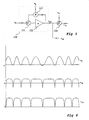
- a raw received co-channel carrier v 0 is passed through a r.f./i.f. stage 101 and through an automatic gain control circuit (AGC) 102 to give v 1 which is termed the co-channel carrier.
- v 0 1 + 2 m cos ⁇ d t + m 2 cos( ⁇ c t + ⁇ m cos ⁇ m t )
- m is the ratio of the interfering carrier to the wanted carrier
- ⁇ c is the angular frequency of the wanted carrier
- ⁇ m is the modulation frequency
- ⁇ d is the difference frequency between the wanted carrier and the interfering carrier
- ⁇ is the depth of modulation.
- v 1 is thus 1 + 2 m cos ⁇ d t + m 2 1 + m 2 cos( ⁇ c t + ⁇ m cos ⁇ m t )
- the denominator function v 8 from the circuit of Fig. 2 and the numerator function v 9 from the circuit of Fig. 3 are processed as follows, with reference to Fig. 5.
- the denominator function v 8 and the numerator function v 9 are processed in an amplitude-locked loop (ALL) circuit 110.
- the ALL circuit 110 comprises an adder 111, an operational amplifier 112 and a multiplier 113.
- the quotient function v 10 is passed to an adder 114 to which there is also input a dc signal v 11
- the signal v 11 has a value of 1 volt.
- the signals v 10 and v 12 are used to condition an fm demodulator as illustrated in Fig. 8.
- a PLL demodulator 117 the input to which is the stabilised output of the AGC circuit 102 of Fig. 1, that is, the co-channel carrier v 1 , produces an output v 13 being a combination of the dominant carrier and the subdominant carrier, the dominant being an unmodulated carrier and the subdominant carrier being a modulated carrier.
- the fm demodulator comprises a subdominant channel 121 and a dominant channel 122.
- the subdominant channel 121 comprises a multiplier 123 fed by signal v 10 and signal v 13 .
- the output of the multiplier 123 (signal v 14 ) is fed through a low pass filter 125 to give a signal v 15 being the recovered sub-dominant signal which is passed to a level conditioner 127 which has a second input being the filtered twice-squared carrier signal v 6 .
- the output of the level conditioner 127 is sub-dominant signal v 16 free of any crosstalk of the dominant carrier, and restored to its normal value.
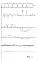
- the waveforms for the sub-dominant channel 121 are shown in Fig. 9, when the sub-dominant, wanted signal is modulated.
- waveform v 23 multiplied by signal v 10 results in suppression of the dominant signal, as illustrated in waveform v 25 .
- the dominant channel 122 comprises a multiplier 124 fed by signal v 12 and signal v 13 to give output v 17 .
- the output of multiplier 124 (v 17 ) is fed to adder 128 through low pass filter 126.
- a second input to the adder 128 is the signal v 15 from low pass filter 125 in the subdominant channel 121.
- the output of the adder 128 is thus the dominant carrier free of any crosstalk from the subdominant carrier.
- the waveforms for the dominant channel are shown in Fig. 11.
- the circuit has two distinct outputs.
- the first, v 16 is the recovered subdominant free of any dominant carrier content
- the second, v 19 is the recovered dominant carrier free of any sub-dominant content.
- circuits of the invention thus provide for the separation of two independently modulated co-channel interfering carrier of similar strength and having the same or similar carrier frequency.
Landscapes
- Engineering & Computer Science (AREA)
- Power Engineering (AREA)
- Digital Transmission Methods That Use Modulated Carrier Waves (AREA)
- Noise Elimination (AREA)
Claims (15)
- Eine Methode zur Demodulation von FM-Signalen; die FM-Signale bestehen aus einem Nutzträgersignal und einem Störträgersignal; die Methode besteht aus den Schritten: - Generierung eines ersten Signals (v3) aus einem Anfangssignal (v1), wobei das besagte erste Signal (v3) eine Funktion des Verhältnisses (m) des Störträgers zum Nutzträger und der Augenblicksdifferenz (?d) zwischen der Frequenz des Nutzträgers und des Störträgers ist; Generierung eines zweiten Signals (v4) aus dem besagten ersten Signal (v3) durch Entfernung aller Gleichglieder aus dem besagten ersten Signal (v3); Bildung des mathematischen Quadrats (v5) des besagten zweiten Signals (v4); Generierung eines Gleichglieds (v6) aus dem besagten quadrierten Signal (v5); Bildung einer Zählerfunktion (v9), die eine Funktion des besagten Gleichglieds (v6), des besagten zweiten Signals (v4) und eines DC-Offsets (v7) darstellt; Bildung einer Nennerfunktion (v8), die eine Funktion des besagten ersten Signals (v3) und des besagten DC-Offsets (v7) darstellt; Ausführung einer Division zwischen der besagten Zählerfunktion (v9) und der besagten Nennerfunktion (v8), um eine Quotientenfunktion (v10) zu bilden; Generierung, aus besagtem Anfangssignal, eines demodulierten FM-Signals (v13), das eine Kombination des Nutzträgersignals und des Störträgersignals darstellt; Multiplizierung der besagten Quotientenfunktion (v10) mit dem besagten demodulierten FM-Signal (v13), um ein erstes Zwischensignal (v14) zu generieren; Weiterleitung des besagten ersten Zwischensignals (v14) durch einen Tiefpassfilter, um ein erstes gefiltertes Signal (v15) zu generieren; und Multiplizierung des besagten ersten gefilterten Signals (v15) mit dem besagten Gleichglied (v6), um ein erstes gewünschtes Signal (v16) zu erhalten.
- Eine Methode wie in Patentanspruch 1 beansprucht, wobei das besagte erste Signal (v3) durch Quadrierung eines Anfangssignals (v1) generiert wird, um ein quadriertes Anfangssignal zu erhalten (v2), und Weiterleitung des besagten quadrierten Anfangssignals (v2) durch einen Tiefpassfilter (104).
- Eine Methode wie in Patentanspruch 2 beansprucht, wobei das besagte Anfangssignal (v1) dadurch entsteht, indem ein Eingangsgleichkanalträger (v0) durch eine automatische Verstärkungsregelungsschaltung (102) geleitet wird.
- Eine Methode wie in allen vorstehenden Patentansprüchen beansprucht, wobei die besagte Quotientenfunktion (v10) dadurch gebildet wird, indem die besagte Zählerfunktion (v9) durch die besagte Nennerfunktion (v8) in einer Amplitudenregelschleifenschaltung (110) geteilt wird.
- Eine Methode wie entweder in Patentanspruch 3 oder Patentanspruch 4 beansprucht, wobei das besagte demodulierte FM-Signal (v13) dadurch generiert wird, indem das besagte Anfangssignal (v1) durch eine Phasenregelschleifenschaltung (117) geleitet wird.
- Eine Methode wie in allen vorherstehenden Patentansprüchen beansprucht, inklusive des Schrittes der Hinzufügung einer Gleichspannung (v11) zu der besagten Quotientenfunktion (v10), um ein modifiziertes Quotientensignal (v12) zu generieren.
- Eine Methode wie in Patentanspruch 6 beansprucht, inklusive des Schrittes der Multiplizierung des besagten modifizierten Quotientensignals (v12) mit dem besagten demodulierten Signal (v13), um ein zweites Zwischensignal (v17) zu erhalten.
- Eine Methode wie in Patentanspruch 7 beansprucht, inklusive der Weiterleitung des besagten zweiten Zwischensignals (v17) durch einen Tiefpassfilter (126), um ein zweites gefiltertes Signal (v18) zu erhalten, und Subtrahierung des besagten ersten gefilterten Signals (v15) von dem besagten zweiten gefilterten Signal (v18), um ein zweites gewünschtes Signal (v19) zu erhalten.
- Eine Schaltung zur Demodulation von FM-Signalen; die FM-Signale bestehen aus einem Nutzträgersignal und einem Störträgersignal; die Schaltung besteht aus Hilfsmitteln (102, 103, 104) zur Generierung eines ersten Signals (v3) aus einem Anfangssignal (v1), wobei das besagte erste Signal (v3) eine Funktion des Verhältnisses (m) des Störträgers zum Nutzträger und der Augenblicksdifferenz (?d) zwischen der Frequenz des Nutzträgers und des Störträgers ist; Hilfsmitteln (105) zur Generierung eines zweiten Signals (v4) aus dem besagten ersten Signal (v3) durch Entfernung aller Gleichglieder aus dem besagten ersten Signal (v3); einer Quadrierschaltung (106) zur Bildung des mathematischen Quadrats (v5) des besagten zweiten Signals (v4); Hilfsmitteln (107) zur Generierung eines Gleichglieds (v6) aus dem besagten quadrierten Signal (v5); Hilfsmittel (109) zur Bildung einer Zählerfunktion (v9), die eine Funktion des besagten Gleichglieds (v6), des besagten zweiten Signals (v4) und eines DC-Offsets (v7) darstellt; Hilfsmittel (108) zur Bildung einer Nennerfunktion (v8), die eine Funktion des besagten ersten Signals (v3) und des besagten DC-Offsets (v7) darstellt; einer Divisionsschaltung (110) zur Ausführung einer Division zwischen der besagten Zählerfunktion (v9) und der besagten Nennerfunktion (v8), um eine Quotientenfunktion (v10) zu bilden; Hilfsmittel (117) zur Generierung, aus besagtem Anfangssignal, eines demodulierten FM-Signals (v13) durch die Kombination des Nutzträgersignals mit dem Störträgersignal; einer Multiplizierungsschaltung (123) zur Multiplizierung der besagten Quotientenfunktion (v10) mit dem besagten demodulierten FM-Signal (v13), um ein erstes Zwischensignal (v14) zu generieren; einem Tiefpassfilter (125), der das besagte erste Zwischensignal (v14) als Eingangssignal erhält und ein erstes gefiltertes Signal (v15) als Ausgangssignal wieder ausgibt; und einer Multiplizierungsschaltung (127) zur Multiplizierung des besagten ersten gefilterten Signals (v15) mit dem besagten Gleichglied (v6), um ein erstes gewünschtes Signal (v16) zu erhalten.
- Eine Schaltung wie in Patentanspruch 9 beansprucht, bei der das besagte Hilfsmittel zur Generierung des besagten zweiten Signals (v4) aus dem besagten ersten Signal (v3) ein Hochpassfilter (105) ist.
- Eine Schaltung wie entweder in Patentanspruch 9 oder Patentanspruch 10 beansprucht, bei der das besagte Hilfsmittel zur Generierung des besagten Gleichglieds (v6) ein Tiefpassfilter (107) ist.
- Eine Schaltung wie in einem der Patentansprüche 9 bis 11 beansprucht, bei der das besagte Hilfsmittel zur Generierung der besagten Zählerfunktion (v9) eine Additionsschaltung (109) ist.
- Eine Schaltung wie in einem der Patentansprüche 9 bis 12 beansprucht, bei der das besagte Hilfsmittel zur Generierung der besagten Nennerfunktion (v8) eine Additionsschaltung (109) ist.
- Eine Schaltung wie in einem der Patentansprüche 9 bis 13 beansprucht, bei der das besagte Hilfsmittel zur Generierung der besagten Divisionsschaltung (110) eine Amplitudenregelschleifenschaltung ist.
- Eine Schaltung wie in einem der Patentansprüche 9 bis 14 beansprucht, bei der das besagte Hilfsmittel zur Generierung des besagten demodulierten FM-Signals (v13) eine Phasenregelschleifenschaltung (117) beinhaltet.
Applications Claiming Priority (3)
| Application Number | Priority Date | Filing Date | Title |
|---|---|---|---|
| GB9804354 | 1998-03-03 | ||
| GBGB9804354.0A GB9804354D0 (en) | 1998-03-03 | 1998-03-03 | Improvements in FM demodulation circuits |
| PCT/GB1999/000629 WO1999045635A1 (en) | 1998-03-03 | 1999-03-03 | Electronic circuits |
Publications (2)
| Publication Number | Publication Date |
|---|---|
| EP1066677A1 EP1066677A1 (de) | 2001-01-10 |
| EP1066677B1 true EP1066677B1 (de) | 2005-11-30 |
Family
ID=10827816
Family Applications (1)
| Application Number | Title | Priority Date | Filing Date |
|---|---|---|---|
| EP99938020A Expired - Lifetime EP1066677B1 (de) | 1998-03-03 | 1999-03-03 | Elektronische schaltungen |
Country Status (6)
| Country | Link |
|---|---|
| US (1) | US6615029B1 (de) |
| EP (1) | EP1066677B1 (de) |
| AU (1) | AU3263399A (de) |
| DE (1) | DE69928653T2 (de) |
| GB (1) | GB9804354D0 (de) |
| WO (1) | WO1999045635A1 (de) |
Families Citing this family (1)
| Publication number | Priority date | Publication date | Assignee | Title |
|---|---|---|---|---|
| US20080063122A1 (en) * | 2006-09-07 | 2008-03-13 | Gwo-Jia Jong | Method for suppressing co-channel interference from different frequency |
Family Cites Families (5)
| Publication number | Priority date | Publication date | Assignee | Title |
|---|---|---|---|---|
| JPS5845216B2 (ja) * | 1977-06-29 | 1983-10-07 | 日本ビクター株式会社 | マルチパス歪の除去回路 |
| JPS5914393B2 (ja) | 1978-07-05 | 1984-04-04 | 三井造船株式会社 | 船底扉の開閉装置 |
| JPS56106434A (en) * | 1980-01-29 | 1981-08-24 | Sony Corp | Eliminating circuit of multipath distortion |
| JPH05506754A (ja) | 1990-01-23 | 1993-09-30 | ザ コート オブ ザ ユニバーシティ オブ ペイズリー | 振幅ロックループ回路 |
| US5778310A (en) * | 1995-11-30 | 1998-07-07 | Northern Telecom Limited | Co-channel interference reduction |
-
1998
- 1998-03-03 GB GBGB9804354.0A patent/GB9804354D0/en not_active Ceased
-
1999
- 1999-03-03 AU AU32633/99A patent/AU3263399A/en not_active Abandoned
- 1999-03-03 WO PCT/GB1999/000629 patent/WO1999045635A1/en active IP Right Grant
- 1999-03-03 US US09/623,610 patent/US6615029B1/en not_active Expired - Fee Related
- 1999-03-03 EP EP99938020A patent/EP1066677B1/de not_active Expired - Lifetime
- 1999-03-03 DE DE69928653T patent/DE69928653T2/de not_active Expired - Fee Related
Also Published As
| Publication number | Publication date |
|---|---|
| WO1999045635A1 (en) | 1999-09-10 |
| DE69928653T2 (de) | 2006-08-24 |
| GB9804354D0 (en) | 1998-04-22 |
| AU3263399A (en) | 1999-09-20 |
| US6615029B1 (en) | 2003-09-02 |
| DE69928653D1 (de) | 2006-01-05 |
| EP1066677A1 (de) | 2001-01-10 |
Similar Documents
| Publication | Publication Date | Title |
|---|---|---|
| US5483695A (en) | Intermediate frequency FM receiver using analog oversampling to increase signal bandwidth | |
| JP3478508B2 (ja) | 無線通信装置 | |
| EP0124949B1 (de) | Mischeranordnung die eine erste und eine zweite Quadratur-Mischstufe enthält | |
| JPH0628338B2 (ja) | フエーズロツクドループ及びそれを用いる直接混合同期am受信機 | |
| EP0087123A2 (de) | Signalempfänger mit verbesserter Selektivität | |
| JP3169690B2 (ja) | 受信装置 | |
| US7292694B2 (en) | Noise reduction in a stereo receiver | |
| EP1276257B1 (de) | DRM/AM Simulcast | |
| EP1066677B1 (de) | Elektronische schaltungen | |
| Costas | Synchronous communications | |
| EP1061654B1 (de) | Rauschdetektion in einem Frequenzdemodulierten FM Rundfunksignal | |
| US4406922A (en) | Stereo broadcast system | |
| JPS6130347Y2 (de) | ||
| US7046811B1 (en) | Stereo demultiplexer | |
| EP0293828B1 (de) | Schaltungsanordnung zum Demodulieren DSB-modulierter Signale und Verfahren dafür | |
| US3643165A (en) | Modulated carrier wave communication apparatus | |
| US4680794A (en) | AM stereo system with modified spectrum | |
| CA1057357A (en) | Compatible am stereophonic receivers | |
| KR820001531B1 (ko) | 무선방송 시스템용 수신기 | |
| CA1067154A (en) | Carrier isolation system | |
| US6023614A (en) | Method for decoding a suppressed-carrier modulated signal in the presence of a pilot tone, particularly for FM signals | |
| KR930001829B1 (ko) | 직교캐리어를 이용한 잡음 제거회로 | |
| CA1252514A (en) | Compatible am broadcast/data transmission system | |
| EP1071232A1 (de) | Stereo-Multiplex-Signalübertragung mit einer Einseitenbandmodulation des Stereo-Differenzsignals für frequenzmodulierten Rundfunksystem | |
| KR820001333B1 (ko) | 양립식 am스테레오 신호수신기 |
Legal Events
| Date | Code | Title | Description |
|---|---|---|---|
| PUAI | Public reference made under article 153(3) epc to a published international application that has entered the european phase |
Free format text: ORIGINAL CODE: 0009012 |
|
| 17P | Request for examination filed |
Effective date: 20000915 |
|
| AK | Designated contracting states |
Kind code of ref document: A1 Designated state(s): DE FR GB IT |
|
| 17Q | First examination report despatched |
Effective date: 20030620 |
|
| GRAP | Despatch of communication of intention to grant a patent |
Free format text: ORIGINAL CODE: EPIDOSNIGR1 |
|
| DAX | Request for extension of the european patent (deleted) | ||
| RAP1 | Party data changed (applicant data changed or rights of an application transferred) |
Owner name: THE COURT OF THE UNIVERSITY OF PAISLEY |
|
| GRAS | Grant fee paid |
Free format text: ORIGINAL CODE: EPIDOSNIGR3 |
|
| GRAA | (expected) grant |
Free format text: ORIGINAL CODE: 0009210 |
|
| AK | Designated contracting states |
Kind code of ref document: B1 Designated state(s): DE FR GB IT |
|
| REG | Reference to a national code |
Ref country code: GB Ref legal event code: FG4D |
|
| REF | Corresponds to: |
Ref document number: 69928653 Country of ref document: DE Date of ref document: 20060105 Kind code of ref document: P |
|
| ET | Fr: translation filed | ||
| PLBE | No opposition filed within time limit |
Free format text: ORIGINAL CODE: 0009261 |
|
| STAA | Information on the status of an ep patent application or granted ep patent |
Free format text: STATUS: NO OPPOSITION FILED WITHIN TIME LIMIT |
|
| 26N | No opposition filed |
Effective date: 20060831 |
|
| PGFP | Annual fee paid to national office [announced via postgrant information from national office to epo] |
Ref country code: GB Payment date: 20090130 Year of fee payment: 11 |
|
| PGFP | Annual fee paid to national office [announced via postgrant information from national office to epo] |
Ref country code: IT Payment date: 20090226 Year of fee payment: 11 Ref country code: DE Payment date: 20090209 Year of fee payment: 11 |
|
| PGFP | Annual fee paid to national office [announced via postgrant information from national office to epo] |
Ref country code: FR Payment date: 20090210 Year of fee payment: 11 |
|
| GBPC | Gb: european patent ceased through non-payment of renewal fee |
Effective date: 20100303 |
|
| REG | Reference to a national code |
Ref country code: FR Ref legal event code: ST Effective date: 20101130 |
|
| PG25 | Lapsed in a contracting state [announced via postgrant information from national office to epo] |
Ref country code: FR Free format text: LAPSE BECAUSE OF NON-PAYMENT OF DUE FEES Effective date: 20100331 |
|
| PG25 | Lapsed in a contracting state [announced via postgrant information from national office to epo] |
Ref country code: DE Free format text: LAPSE BECAUSE OF NON-PAYMENT OF DUE FEES Effective date: 20101001 |
|
| PG25 | Lapsed in a contracting state [announced via postgrant information from national office to epo] |
Ref country code: IT Free format text: LAPSE BECAUSE OF NON-PAYMENT OF DUE FEES Effective date: 20100303 Ref country code: GB Free format text: LAPSE BECAUSE OF NON-PAYMENT OF DUE FEES Effective date: 20100303 |