EP1066677B1 - Electronic circuits - Google Patents
Electronic circuits Download PDFInfo
- Publication number
- EP1066677B1 EP1066677B1 EP99938020A EP99938020A EP1066677B1 EP 1066677 B1 EP1066677 B1 EP 1066677B1 EP 99938020 A EP99938020 A EP 99938020A EP 99938020 A EP99938020 A EP 99938020A EP 1066677 B1 EP1066677 B1 EP 1066677B1
- Authority
- EP
- European Patent Office
- Prior art keywords
- signal
- function
- generating
- circuit
- carrier
- Prior art date
- Legal status (The legal status is an assumption and is not a legal conclusion. Google has not performed a legal analysis and makes no representation as to the accuracy of the status listed.)
- Expired - Lifetime
Links
Images


Classifications
-
- H—ELECTRICITY
- H03—ELECTRONIC CIRCUITRY
- H03D—DEMODULATION OR TRANSFERENCE OF MODULATION FROM ONE CARRIER TO ANOTHER
- H03D3/00—Demodulation of angle-, frequency- or phase- modulated oscillations
- H03D3/001—Details of arrangements applicable to more than one type of frequency demodulator
- H03D3/002—Modifications of demodulators to reduce interference by undesired signals
Description
- This invention relates to electronic circuits and more particularly to the demodulation of frequency modulated (fm) radio signals.
- Whereas electronic circuits for the demodulation of fm signals have been known since the use of fm for radio broadcasting began in the nineteen thirties, there has been a major problem with all existing demodulators, namely, that if two fm transmissions reach the receiver at the same carrier frequency and amplitude, mutual destruction of both transmissions occurs and all intelligibility is lost.
- This is a fundamental property of fm demodulators which use saturating circuits prior to the fm demodulator to remove amplitude noise effects from disturbing the wanted signal.
- This effect is called co-channel interference especially when the second interfering transmission is a different station. There are four other types of similar interference which result in complete loss of signal.
- The first type is called multipath transmission when a delayed version of the same signal is received at the antenna.
- The second type is called quasi-sync transmission when the same message is being transmitted on the same frequency but from another transmitter location. At the overlap of the reception, all intelligibility is lost.
- The third type is called self-jamming or deliberate-jamming when an unmodulated carrier is transmitted at equal amplitude to the desired modulated carrier. This commonly occurs in military circumstances including laser Dopplerimetry.
- The fourth type is called the threshold condition, when the signal is very weak relative to general noise levels. There is a disproportionate increase in demodulated noise levels which causes loss of intelligibility.
- These problems exist for all of fm transmissions whether in an analogue or digital format and include spread spectrum technologies.
- Demodulation techniques are known which mitigate the first and second types of interference, ie multipath and quasi-sync. In these circuits, the output is the sum of the two carriers and there is no requirement to separate the two carriers since the same information is carried by them both. However, these known techniques are not suitable for separating a pair of independently modulated co-channel interfering carriers, that is, two carriers of similar strength (1-15dB difference) and having the same or similar carrier frequency. The document "PETTIGREW A: 'DEMODULATION A NEW APPROACH' ELECTRONICS WORLD AND WIRELESS WORLD, vol. 101, no. 1717, 1 December 1995, pages 1026-1031, XP000548985" discusses such a demodulation method involving an amplitude-locked loop used in conjunction with a phase-locked loop.
- It is an object of the present invention to provide a method and apparatus for minimising and, in some cases, eliminating the aforementioned problems from fm demodulators.
- This object is achieved by the method according to claim 1 and the corresponding circuit according to claim 9.
- Embodiments of the present invention will now be described, by way of example, with reference to the accompanying drawings, in which:-
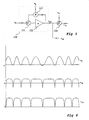
- Fig. 1 is a block diagram of the initial stage of the circuit of the invention;
- Fig. 2 is a block diagram of the denominator function generator stage;
- Fig. 3 is a block diagram of the numerator function generator stage;
- Fig. 4 are waveforms of the different signals of the block diagrams of Figs 1 to 3;
- Fig. 5 is a block diagram of the amplitude-locked loop (ALL) circuit for generating the quotient function of the invention;
- Fig. 6 are waveforms of the signals of the circuit of Fig. 5.
- Fig. 7 is a block diagram of a phase-locked loop used in the circuit of the invention;
- Fig. 8 is a block diagram illustrating the dominant and sub-dominant channels of the circuit of the invention; and
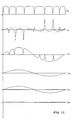
- Figs 9, 10 and 11 illustrate waveforms of the circuit of Fig. 8.
-
- Referring to Fig. 1, a raw received co-channel carrier v0 is passed through a r.f./i.f. stage 101 and through an automatic gain control circuit (AGC) 102 to give v1 which is termed the co-channel carrier.
ωc is the angular frequency of the wanted carrier;
ωm is the modulation frequency;
ωd is the difference frequency between the wanted carrier and the interfering carrier; and
β is the depth of modulation. - The co-channel carrier v1 is passed to a first pure squaring circuit 103 to give v2 termed the pure squared received co-channel carrier, where
- If m' is defined as
- Referring now to Fig. 2, the filtered squared signal v3 is added to a small dc offset v7 in adder 108 to give a denominator function, signal v8,
where - Referring to Fig. 3, v3 is passed to high pass filter 105 to remove the dc content to give v4, where
- Adder 109 serves to add signal v6, signal v4 and subtract the dc offset v7 to give a numerator function v9, where
- The main waveforms of the signals appearing in the circuits of Figs 1 to 3 are illustrated in Fig. 4.
- The denominator function v8 from the circuit of Fig. 2 and the numerator function v9 from the circuit of Fig. 3 are processed as follows, with reference to Fig. 5.
- The denominator function v8 and the numerator function v9 are processed in an amplitude-locked loop (ALL) circuit 110. The ALL circuit 110 comprises an adder 111, an operational amplifier 112 and a multiplier 113. The output of the ALL 110 is a quotient function v10 obtained by dividing the numerator function v9 by the denominator function v8, to give
- The quotient function v10 is passed to an adder 114 to which there is also input a dc signal v11
- In a normalised system, the signal v11 has a value of 1 volt. v10 and v11 combine to give a signal v12, where v12 is defined as v10+1
thus - The main waveforms of the signals appearing in the circuit of Fig. 5 are illustrated in Fig. 6.
- The signals v10 and v12 are used to condition an fm demodulator as illustrated in Fig. 8.
- Referring now to Fig. 7, a PLL demodulator 117, the input to which is the stabilised output of the AGC circuit 102 of Fig. 1, that is, the co-channel carrier v1, produces an output v13 being a combination of the dominant carrier and the subdominant carrier, the dominant being an unmodulated carrier and the subdominant carrier being a modulated carrier.
- Output v13 can be expressed as
- Referring now to Fig. 8, the fm demodulator comprises a subdominant channel 121 and a dominant channel 122.
- The subdominant channel 121 comprises a multiplier 123 fed by signal v10 and signal v13. The output of the multiplier 123 (signal v14) is fed through a low pass filter 125 to give a signal v15 being the recovered sub-dominant signal which is passed to a level conditioner 127 which has a second input being the filtered twice-squared carrier signal v6. The output of the level conditioner 127 is sub-dominant signal v16 free of any crosstalk of the dominant carrier, and restored to its normal value.
- The waveforms for the sub-dominant channel 121 are shown in Fig. 9, when the sub-dominant, wanted signal is modulated.
- In the case where the dominant, unwanted, signal is modulated, as illustrated in Fig. 10, waveform v23 multiplied by signal v10 results in suppression of the dominant signal, as illustrated in waveform v25.
- The dominant channel 122 comprises a multiplier 124 fed by signal v12 and signal v13 to give output v17. The output of multiplier 124 (v17) is fed to adder 128 through low pass filter 126. A second input to the adder 128 is the signal v15 from low pass filter 125 in the subdominant channel 121. The output of the adder 128 is thus the dominant carrier free of any crosstalk from the subdominant carrier. The waveforms for the dominant channel are shown in Fig. 11.
- Thus the circuit has two distinct outputs. The first, v16, is the recovered subdominant free of any dominant carrier content, and the second, v19, is the recovered dominant carrier free of any sub-dominant content.
- The circuits of the invention thus provide for the separation of two independently modulated co-channel interfering carrier of similar strength and having the same or similar carrier frequency.
Claims (15)
- A method for the demodulation of fm signals, the fm signals comprising a wanted carrier signal and an interfering carrier signal, the method comprising the steps of :- generating a first signal (v3) from an initial signal (v1), said first signal (v3) being a function of the ratio (m) of the interfering carrier to the wanted carrier and of the instantaneous difference (ωd) between the frequency of the wanted carrier and the interfering carrier; generating a second signal (v4) from said first signal (v3) by removing any dc value from said first signal (v3); generating the mathematical square (v5) of said second signal (v4) ; generating a dc value (v6) from said squared signal (v5); generating a numerator function (v9) being a function of said dc value (v6), said second signal (v4) and a dc offset (v7); generating a denominator function (v8) being a function of said first signal (v3) and said dc offset (v7); performing a division process between said numerator function (v9) and said denominator function (v8) to generate a quotient function (v10); generating, from said initial signal, a demodulated fm signal (v13) being a combination of the wanted carrier signal and the interfering carrier signal; multiplying together said quotient function (v10) and said demodulated fm signal (v13) to generate a first intermediate output (v14); passing said first intermediate output (v14) through a low pass filter to generate a first filtered output (v15) ; and multiplying said first filtered output (v15) by said dc value (v6) to give a first desired output (v16).
- A method as claimed in Claim 1 wherein said first signal (v3) is generated by squaring an initial signal (v1) to give a squared initial signal (v2), and passing said squared initial signal (v2) through a low pass filter (104).
- A method as claimed in Claim 2 wherein said initial signal (v1) is derived by passing an input co-channel carrier (v0) through an automatic gain control circuit (102).
- A method as claimed in any preceding Claim wherein said quotient function (v10) is generated by dividing said numerator function (v9) by said denominator function (v8) in an Amplitude Locked Loop circuit (110).
- A method as claimed in either Claim 3 or Claim 4 wherein said demodulated fm signal (v13) is generated by passing said initial signal (v1) through a Phase Locked Loop circuit (117).
- A method as claimed in any preceding claim, including the step of adding a dc voltage (v11) to the said quotient function (v10) to generate a modified quotient signal (v12) .
- A method as claimed in claim 6, including the step of multiplying said modified quotient signal (v12) by said demodulated output (v13) to give a second intermediate output (v17).
- A method as claimed in Claim 7, including passing said second intermediate output (v17) through a low pass filter (126) to give a second filtered output (v18) and subtracting from said second filtered output (v18) said first filtered output (v15) to give a second desired output (v19).
- A circuit for demodulating FM signals, the FM signals comprising a wanted carrier signal and an interfering carrier signal, the circuit comprising means (102, 103,104) for generating a first signal (v3) from an initial signal (v1), said first signal (v3) being a function of the ratio (m) of the interfering carrier to the wanted carrier and of the instantaneous difference (ωd) between the frequency of the wanted carrier and the interfering carrier; means (105) for generating a second signal (v4) from said first signal (v3) by removing any dc value from said first signal (v3) ; a squaring circuit (106) for generating the mathematical square (v5) of said second signal (v4); means (107) for generating a dc value (v6) from said squared signal (v5) ; means (109) for generating a numerator function (v9) being a function of said dc value (v6), said second signal (v4) and a dc offset (v7); means (108) for generating a denominator function (v8) being a function of said first signal (v3) and said dc offset (v7); a division circuit (110) for performing a division process between said numerator function (v9) and said denominator function (v8) to generate a quotient function (v10); means (117) for generating, from said initial signal, a demodulated fm signal (v13) by combining the wanted carrier signal and the interfering carrier signal; a multiplier circuit (123) for multiplying together said quotient function (v10) and said demodulated fm signal (v13) to generate a first intermediate output (v14) ; a low pass filter (125) receiving said first intermediate output (v14) as input and providing as output a first filtered output (v15); and a multiplier circuit (127) for multiplying said first filtered output (v15) by said dc value (v6) to give a first desired output (v16) .
- A circuit as claimed in Claim 9, wherein said means for generating said second signal (v4) from said first signal (v3) is a high pass filter (105) .
- A circuit as claimed in either of Claims 9 or 10, wherein said means for generating said dc value (v6) is a low pass filter (107).
- A circuit as claimed in any one of Claims 9 to 11, wherein said means for generating said numerator function (v9) is an adder circuit (109).
- A circuit as claimed in any one of Claims 9 to 12, wherein said means for generating said denominator function (v8) is an adder circuit (108).
- A circuit as claimed in any of Claims 9 to 13, wherein said division circuit (110) is an Amplitude Locked Loop Circuit.
- A circuit as claimed in any of claims 9 to 14, wherein said means for generating said demodulated fm signal (v13) comprises a Phase Locked Loop circuit (117) .
Applications Claiming Priority (3)
| Application Number | Priority Date | Filing Date | Title |
|---|---|---|---|
| GB9804354 | 1998-03-03 | ||
| GBGB9804354.0A GB9804354D0 (en) | 1998-03-03 | 1998-03-03 | Improvements in FM demodulation circuits |
| PCT/GB1999/000629 WO1999045635A1 (en) | 1998-03-03 | 1999-03-03 | Electronic circuits |
Publications (2)
| Publication Number | Publication Date |
|---|---|
| EP1066677A1 EP1066677A1 (en) | 2001-01-10 |
| EP1066677B1 true EP1066677B1 (en) | 2005-11-30 |
Family
ID=10827816
Family Applications (1)
| Application Number | Title | Priority Date | Filing Date |
|---|---|---|---|
| EP99938020A Expired - Lifetime EP1066677B1 (en) | 1998-03-03 | 1999-03-03 | Electronic circuits |
Country Status (6)
| Country | Link |
|---|---|
| US (1) | US6615029B1 (en) |
| EP (1) | EP1066677B1 (en) |
| AU (1) | AU3263399A (en) |
| DE (1) | DE69928653T2 (en) |
| GB (1) | GB9804354D0 (en) |
| WO (1) | WO1999045635A1 (en) |
Families Citing this family (1)
| Publication number | Priority date | Publication date | Assignee | Title |
|---|---|---|---|---|
| US20080063122A1 (en) * | 2006-09-07 | 2008-03-13 | Gwo-Jia Jong | Method for suppressing co-channel interference from different frequency |
Family Cites Families (5)
| Publication number | Priority date | Publication date | Assignee | Title |
|---|---|---|---|---|
| JPS5845216B2 (en) * | 1977-06-29 | 1983-10-07 | 日本ビクター株式会社 | Multipath distortion removal circuit |
| JPS5914393B2 (en) | 1978-07-05 | 1984-04-04 | 三井造船株式会社 | Bottom door opening/closing device |
| JPS56106434A (en) * | 1980-01-29 | 1981-08-24 | Sony Corp | Eliminating circuit of multipath distortion |
| JPH05506754A (en) | 1990-01-23 | 1993-09-30 | ザ コート オブ ザ ユニバーシティ オブ ペイズリー | amplitude locked loop circuit |
| US5778310A (en) | 1995-11-30 | 1998-07-07 | Northern Telecom Limited | Co-channel interference reduction |
-
1998
- 1998-03-03 GB GBGB9804354.0A patent/GB9804354D0/en not_active Ceased
-
1999
- 1999-03-03 WO PCT/GB1999/000629 patent/WO1999045635A1/en active IP Right Grant
- 1999-03-03 EP EP99938020A patent/EP1066677B1/en not_active Expired - Lifetime
- 1999-03-03 DE DE69928653T patent/DE69928653T2/en not_active Expired - Fee Related
- 1999-03-03 AU AU32633/99A patent/AU3263399A/en not_active Abandoned
- 1999-03-03 US US09/623,610 patent/US6615029B1/en not_active Expired - Fee Related
Also Published As
| Publication number | Publication date |
|---|---|
| AU3263399A (en) | 1999-09-20 |
| WO1999045635A1 (en) | 1999-09-10 |
| EP1066677A1 (en) | 2001-01-10 |
| US6615029B1 (en) | 2003-09-02 |
| DE69928653D1 (en) | 2006-01-05 |
| GB9804354D0 (en) | 1998-04-22 |
| DE69928653T2 (en) | 2006-08-24 |
Similar Documents
| Publication | Publication Date | Title |
|---|---|---|
| US5483695A (en) | Intermediate frequency FM receiver using analog oversampling to increase signal bandwidth | |
| JP3478508B2 (en) | Wireless communication device | |
| EP0124949B1 (en) | Mixer arrangement comprising first and second quadrature mixer stages | |
| JPH0628338B2 (en) | Phase locked loop and direct mixed sync AM receiver using the same | |
| EP0087123A2 (en) | Enhanced selectivity signal receiver | |
| JP3169690B2 (en) | Receiver | |
| US7292694B2 (en) | Noise reduction in a stereo receiver | |
| EP1276257B1 (en) | DRM/AM simulcast | |
| EP1066677B1 (en) | Electronic circuits | |
| Costas | Synchronous communications | |
| EP1061654B1 (en) | Detection of noise in a frequency demodulated fm audio broadcast signal | |
| US4406922A (en) | Stereo broadcast system | |
| JPS6130347Y2 (en) | ||
| US7046811B1 (en) | Stereo demultiplexer | |
| EP0293828B1 (en) | Circuit device for demodulating DSB modulated signals and method therefor | |
| US3643165A (en) | Modulated carrier wave communication apparatus | |
| US4680794A (en) | AM stereo system with modified spectrum | |
| CA1057357A (en) | Compatible am stereophonic receivers | |
| KR820001531B1 (en) | Radio broadcasting system reciever | |
| CA1067154A (en) | Carrier isolation system | |
| US6023614A (en) | Method for decoding a suppressed-carrier modulated signal in the presence of a pilot tone, particularly for FM signals | |
| KR930001829B1 (en) | Circuit for removing noise | |
| CA1252514A (en) | Compatible am broadcast/data transmission system | |
| EP1071232A1 (en) | Stereo multiplex-signal transmission with one single sideband modulation of the stereo-difference signal for frequency modulated broadcast system | |
| KR820001333B1 (en) | Receiver for compatible am stereo signals |
Legal Events
| Date | Code | Title | Description |
|---|---|---|---|
| PUAI | Public reference made under article 153(3) epc to a published international application that has entered the european phase |
Free format text: ORIGINAL CODE: 0009012 |
|
| 17P | Request for examination filed |
Effective date: 20000915 |
|
| AK | Designated contracting states |
Kind code of ref document: A1 Designated state(s): DE FR GB IT |
|
| 17Q | First examination report despatched |
Effective date: 20030620 |
|
| GRAP | Despatch of communication of intention to grant a patent |
Free format text: ORIGINAL CODE: EPIDOSNIGR1 |
|
| DAX | Request for extension of the european patent (deleted) | ||
| RAP1 | Party data changed (applicant data changed or rights of an application transferred) |
Owner name: THE COURT OF THE UNIVERSITY OF PAISLEY |
|
| GRAS | Grant fee paid |
Free format text: ORIGINAL CODE: EPIDOSNIGR3 |
|
| GRAA | (expected) grant |
Free format text: ORIGINAL CODE: 0009210 |
|
| AK | Designated contracting states |
Kind code of ref document: B1 Designated state(s): DE FR GB IT |
|
| REG | Reference to a national code |
Ref country code: GB Ref legal event code: FG4D |
|
| REF | Corresponds to: |
Ref document number: 69928653 Country of ref document: DE Date of ref document: 20060105 Kind code of ref document: P |
|
| ET | Fr: translation filed | ||
| PLBE | No opposition filed within time limit |
Free format text: ORIGINAL CODE: 0009261 |
|
| STAA | Information on the status of an ep patent application or granted ep patent |
Free format text: STATUS: NO OPPOSITION FILED WITHIN TIME LIMIT |
|
| 26N | No opposition filed |
Effective date: 20060831 |
|
| PGFP | Annual fee paid to national office [announced via postgrant information from national office to epo] |
Ref country code: GB Payment date: 20090130 Year of fee payment: 11 |
|
| PGFP | Annual fee paid to national office [announced via postgrant information from national office to epo] |
Ref country code: IT Payment date: 20090226 Year of fee payment: 11 Ref country code: DE Payment date: 20090209 Year of fee payment: 11 |
|
| PGFP | Annual fee paid to national office [announced via postgrant information from national office to epo] |
Ref country code: FR Payment date: 20090210 Year of fee payment: 11 |
|
| GBPC | Gb: european patent ceased through non-payment of renewal fee |
Effective date: 20100303 |
|
| REG | Reference to a national code |
Ref country code: FR Ref legal event code: ST Effective date: 20101130 |
|
| PG25 | Lapsed in a contracting state [announced via postgrant information from national office to epo] |
Ref country code: FR Free format text: LAPSE BECAUSE OF NON-PAYMENT OF DUE FEES Effective date: 20100331 |
|
| PG25 | Lapsed in a contracting state [announced via postgrant information from national office to epo] |
Ref country code: DE Free format text: LAPSE BECAUSE OF NON-PAYMENT OF DUE FEES Effective date: 20101001 |
|
| PG25 | Lapsed in a contracting state [announced via postgrant information from national office to epo] |
Ref country code: IT Free format text: LAPSE BECAUSE OF NON-PAYMENT OF DUE FEES Effective date: 20100303 Ref country code: GB Free format text: LAPSE BECAUSE OF NON-PAYMENT OF DUE FEES Effective date: 20100303 |