EP1059672A2 - Hochspannungsfestigkeit-Halbleiteranordnung und Verfahren zur Herstellung - Google Patents
Hochspannungsfestigkeit-Halbleiteranordnung und Verfahren zur Herstellung Download PDFInfo
- Publication number
- EP1059672A2 EP1059672A2 EP00112400A EP00112400A EP1059672A2 EP 1059672 A2 EP1059672 A2 EP 1059672A2 EP 00112400 A EP00112400 A EP 00112400A EP 00112400 A EP00112400 A EP 00112400A EP 1059672 A2 EP1059672 A2 EP 1059672A2
- Authority
- EP
- European Patent Office
- Prior art keywords
- semi
- insulating film
- region
- withstand voltage
- insulating
- Prior art date
- Legal status (The legal status is an assumption and is not a legal conclusion. Google has not performed a legal analysis and makes no representation as to the accuracy of the status listed.)
- Withdrawn
Links
Images


Classifications
-
- H—ELECTRICITY
- H10—SEMICONDUCTOR DEVICES; ELECTRIC SOLID-STATE DEVICES NOT OTHERWISE PROVIDED FOR
- H10D—INORGANIC ELECTRIC SEMICONDUCTOR DEVICES
- H10D64/00—Electrodes of devices having potential barriers
- H10D64/111—Field plates
- H10D64/115—Resistive field plates, e.g. semi-insulating field plates
-
- H—ELECTRICITY
- H10—SEMICONDUCTOR DEVICES; ELECTRIC SOLID-STATE DEVICES NOT OTHERWISE PROVIDED FOR
- H10P—GENERIC PROCESSES OR APPARATUS FOR THE MANUFACTURE OR TREATMENT OF DEVICES COVERED BY CLASS H10
- H10P14/00—Formation of materials, e.g. in the shape of layers or pillars
- H10P14/60—Formation of materials, e.g. in the shape of layers or pillars of insulating materials
- H10P14/63—Formation of materials, e.g. in the shape of layers or pillars of insulating materials characterised by the formation processes
- H10P14/6302—Non-deposition formation processes
- H10P14/6316—Formation by nitridation, e.g. nitridation of the substrate
-
- H—ELECTRICITY
- H10—SEMICONDUCTOR DEVICES; ELECTRIC SOLID-STATE DEVICES NOT OTHERWISE PROVIDED FOR
- H10P—GENERIC PROCESSES OR APPARATUS FOR THE MANUFACTURE OR TREATMENT OF DEVICES COVERED BY CLASS H10
- H10P14/00—Formation of materials, e.g. in the shape of layers or pillars
- H10P14/60—Formation of materials, e.g. in the shape of layers or pillars of insulating materials
- H10P14/63—Formation of materials, e.g. in the shape of layers or pillars of insulating materials characterised by the formation processes
- H10P14/6302—Non-deposition formation processes
- H10P14/6319—Formation by plasma treatments, e.g. plasma oxidation of the substrate
-
- H—ELECTRICITY
- H10—SEMICONDUCTOR DEVICES; ELECTRIC SOLID-STATE DEVICES NOT OTHERWISE PROVIDED FOR
- H10P—GENERIC PROCESSES OR APPARATUS FOR THE MANUFACTURE OR TREATMENT OF DEVICES COVERED BY CLASS H10
- H10P14/00—Formation of materials, e.g. in the shape of layers or pillars
- H10P14/60—Formation of materials, e.g. in the shape of layers or pillars of insulating materials
- H10P14/63—Formation of materials, e.g. in the shape of layers or pillars of insulating materials characterised by the formation processes
- H10P14/6326—Deposition processes
- H10P14/6328—Deposition from the gas or vapour phase
- H10P14/6329—Deposition from the gas or vapour phase using physical ablation of a target, e.g. physical vapour deposition or pulsed laser deposition
-
- H—ELECTRICITY
- H10—SEMICONDUCTOR DEVICES; ELECTRIC SOLID-STATE DEVICES NOT OTHERWISE PROVIDED FOR
- H10P—GENERIC PROCESSES OR APPARATUS FOR THE MANUFACTURE OR TREATMENT OF DEVICES COVERED BY CLASS H10
- H10P14/00—Formation of materials, e.g. in the shape of layers or pillars
- H10P14/60—Formation of materials, e.g. in the shape of layers or pillars of insulating materials
- H10P14/63—Formation of materials, e.g. in the shape of layers or pillars of insulating materials characterised by the formation processes
- H10P14/6326—Deposition processes
- H10P14/6328—Deposition from the gas or vapour phase
- H10P14/6334—Deposition from the gas or vapour phase using decomposition or reaction of gaseous or vapour phase compounds, i.e. chemical vapour deposition
- H10P14/6336—Deposition from the gas or vapour phase using decomposition or reaction of gaseous or vapour phase compounds, i.e. chemical vapour deposition in the presence of a plasma [PECVD]
-
- H—ELECTRICITY
- H10—SEMICONDUCTOR DEVICES; ELECTRIC SOLID-STATE DEVICES NOT OTHERWISE PROVIDED FOR
- H10P—GENERIC PROCESSES OR APPARATUS FOR THE MANUFACTURE OR TREATMENT OF DEVICES COVERED BY CLASS H10
- H10P14/00—Formation of materials, e.g. in the shape of layers or pillars
- H10P14/60—Formation of materials, e.g. in the shape of layers or pillars of insulating materials
- H10P14/69—Inorganic materials
- H10P14/694—Inorganic materials composed of nitrides
- H10P14/6943—Inorganic materials composed of nitrides containing silicon
- H10P14/69433—Inorganic materials composed of nitrides containing silicon the material being a silicon nitride not containing oxygen, e.g. SixNy or SixByNz
Definitions
- the present invention relates to a high withstand voltage semiconductor device such as an IGBT (insulated gate type bipolar transistor) or a high withstand voltage power IC, and more particularly to realization of high withstand voltage of the surface thereof.
- a high withstand voltage semiconductor device such as an IGBT (insulated gate type bipolar transistor) or a high withstand voltage power IC
- An example thereof is an electrode structure for the purpose of relaxing surface electric field, i.e. a "over-oxide structure”.
- the technique for optimizing it is disclosed in e.g. IEEE Trans. Electron Dev. ED-26, pp. 1098 (1979).
- the resistive film which is a conventional technique is deposited by "electron beam evaporation" in which a silicon source is generally evaporated by electron beams.
- This technique is problematic from the viewpoint of wafer process in that a poor technique in source melting leads to abrupt vaporization because the silicon source is a refractory material to generate inconvenience such as production of a projection on the wafer surface.
- SIPOS Semi-Insulating Polycrystalline Silicon
- the semi-insulating film is formed by reacting silane (SiH 4 ) and dinitrogen oxide (N 2 O)in an atmosphere of N 2 , through the reduced pressure CVD technique, generally at 600 °C.
- the semi-insulating film cannot be deposited after an Al electrode has been formed, but it must be deposited before the Al electrode is formed. Further, it has been proposed to use a semi-insulating silicon nitride film by the plasma CVD taking advantage of that it can be formed at a low temperature (IEEE Tran. On Electron Device, Vol. 37, No. 6, p1522, June (1999)).
- this technique may suffer from inconvenience that the semi-insulating silicon nitride film may be corroded in a reliability test after mold resin sealing.
- the high withstand voltage semiconductor device having such an unstable semi-insulating silicon nitride film provide poor reliability in the withstand voltage characteristic.
- Fig. 5A is a sectional view of the main portion of a conventional high withstand voltage semiconductor device
- Fig. 5B is a distribution graph of composition elements of the semi-insulating silicon nitride film and insulating silicon nitride film, which have been deposited by the conventional technique.
- Fig. 5A is a sectional view of the main portion of a planar diode.
- an n+ cathode region 2 and a p+ anode region 3 are formed, on which a cathode electrode 5 and an anode electrode 6 are formed, respectively.
- An oxide film 4 serving as a surface protection film is formed partially on the n+ cathode region 2, p+ anode region 3 and n-type semiconductor substrate 1 sandwiched between these regions.
- a semi-insulating silicon nitride film 27 and an insulating silicon nitride film 28, which are field plate films, are formed.
- the semi-insulating film 27 is deposited by the plasma CVD technique, and in order to assure the reliability, it is covered with the insulating silicon nitride film 28.
- the insulting silicon nitride film 28 is formed on the semi-insulating silicon nitride film 27 by the plasma CVD using silane (SiO 4 ) and ammonia (NH 3 )or nitrogen (N 2 ).
- An object of the invention is to provide a high withstand voltage semiconductor device which can solve the above problem and improve the reliability of the withstand voltage characteristic, and a method of manufacturing it.
- a high withstand voltage semiconductor device wherein a first region having a first conduction type and a second region having a second conduction type are formed in a surface layer of a semiconductor substrate having the first conduction type, comprises a semi-insulating film formed on the semiconductor substrate sandwiched between the first region and second region, and an insulating film formed on the semi-insulating film.
- the semi-insulating film is formed through an insulating layer on the semiconductor substrate.
- the semi-insulating film covers the first electrode formed on the first region, the second electrode formed on the second region and an edge of each of the first and the second electrode.
- the semi-insulating film contains at least Si, N and H atoms and the insulating film is a film formed by nitriding the semi-insulating film within nitrogen plasma.
- the insulating film is a film formed by nitriding the surface layer of the semi-insulating film within nitrogen plasma.
- the semi-insulating film contains at least Si, N and H atoms
- the insulating film is a film deposited by reactive sputtering not containing H atoms and containing at least Si and N atoms as main elements.
- a method of manufacturing a high withstand voltage semiconductor device wherein a first region having a first conduction type and a second region having a second conduction type are formed in a surface layer of a semiconductor substrate having the first conduction type comprises the steps of forming a semi-insulating film containing at least Si, N and H atoms on the semiconductor substrate sandwiched between the first region and the second region and nitriding a surface layer of the semi-insulating film in an atmosphere of nitrogen plasma to form an insulating film.
- a method of manufacturing a high withstand voltage semiconductor device wherein a first region having a first conduction type and a second region having a second conduction type are formed in a surface layer of a semiconductor substrate having the first conduction type comprises the steps: forming a semi-insulating film containing at least Si, N and H atoms on the semiconductor substrate sandwiched between the first region and the second region and forming an insulating film by the reactive sputtering technique not containing H and containing at least Si and N atoms as main elements.
- the manufacturing method comprises the steps of forming an insulating layer on the semiconductor substrate arid forming a semi-insulating film containing at least Si, N and H atoms on the insulating layer.
- the insulating silicon nitride film used as a protection film can be formed in an atmosphere not containing active H atoms so that it can be formed without changing the film quality of the underlying semi-insulating silicon nitride film.
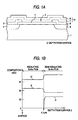
- Figs. 1A and 1B show a first embodiment of the invention.
- Fig. 1A is a sectional of the main part of a high withstand voltage semiconductor device and
- Fig. 1B is a distribution graph of composition elements in a depth direction of the semi-insulating film and insulating film.
- the semi-insulating film is referred to as a semi-insulating silicon nitride film and the insulating film is referred to as an insulating silicon nitride film.
- the high withstand voltage semiconductor device illustrated here is a diode having a horizontal planar structure.
- this embodiment can be applied to a semiconductor device having a planar structure such as a horizontal or vertical MOSFET or IGBT.
- n+ cathode region 2 and a p+ anode region 3 are formed, on which a cathode electrode 5 and an anode electrode 6 are formed, respectively.
- An oxide film 4 serving as a surface protection film is formed partially on the n+ cathode region 2, p+ anode region 3 and n-type semiconductor substrate 1 sandwiched between these regions.
- the film composition of the surface layer of the semi-insulating silicon nitride film 10 is changed into e.g. a stoichiometric silicon nitride film (Si 3 N 4 ) having a thickness of 0.1 ⁇ m to form an insulating silicon nitride film 8.
- the composition of the semi-insulating silicon nitride film 7 having a thickness of about 0.9 ⁇ m which is located beneath the insulating silicon nitride film 8 remains that of the semi-insulating silicon nitride film 10 before the insulating silicon nitride 7 is formed.
- the presence of the insulating silicon nitride film 8 prevents the semi-insulating silicon nitride film 7 from being exposed to the environment.
- the insulating silicon nitride film 8 can be formed without changing the film composition of the underlying semi-insulating silicon nitride film 7, particularly the density of H.
- the semi-insulating film silicon nitride film 7, whose composition does not almost change, serves as a field plate so that the intervals between equipotential lines in the depletion layer extended in the n-type semiconductor substrate 1 are equalized to relax the concentration of electric field in the surface.
- Fig. 2 is a sectional view of the high withstand voltage semiconductor device according to the second embodiment of the invention.
- the sectional view illustrates a level difference at the end of wiring.
- a semi-insulating SixNyHz film (R-SiN 21) which is a semi-insulating silicon nitride film is deposited on a n-type semiconductor substrate 1 and a wiring 23 made of aluminum. Thereafter, by the N 2 plasma processing, the surface layer of R-SiN 21 is reformed into an insulating SixNyHz (R-SiN+N 22) which is an insulating silicon nitride film.
- the initial semi-insulating SixNyHz film (R-SiN 21) is deposited under the deposition condition of SiN 4 of 275 sccm, NH 3 of 100 sccm, carrier gas Ar of 1500 sccm, gas pressure of 0.4 Torr, substrate temperature of 320 °C, RF power of 0.38 kW (50 kHz), and deposition time of 205 sec. This provides the film thickness of 0. 1 ⁇ m.
- the surface layer of the semi-insulating SixNyHz film (R-SiN 21) is reformed into the insulating SixNyHz (R-SiN+N 22). It is reformed under the condition of N 2 of 275 sccm, carrier gas N 2 of 1120 sccm, gas pressure of 0.4 torr., substrate temperature of 320 °C, RF power of 0. 38 kW (50 kHz) and deposition time of 2400 sec. This reforms the surface layer of the semi-insulating SixNyHz film (R-SiN 21) into the insulating SixNyHz (R-SiN+N 22) having a thickness of 0.018 ⁇ m.
- the semi-insulating SixNyHz film (I-SiN) is deposited under the deposition condition of SiN 4 of 202 sccm, NH 3 of 380 sccm, carrier gas Ar of 1938 sccm, gas pressure of 0.4 Torr, substrate temperature of 300 °C, RF power of 0.36 kW (50 kHz), and deposition time of 20114 sec.
- the composition analysis by ESCA of the film thus deposited is shown in Table 1.
- a crack 25 which is generated in the semi-insulating silicon nitride film (R-SiN 21) covering a step 24 at the tip of the wiring 23, can be reformed into the semi-insulating silicon nitride film (R-SiN+N 2 22) by the N 2 plasma processing, which is brought into intimate contact with the semi-insulating silicon nitride film (R-SiN 21). This prevent moisture from invading into the step 24. This was confirmed by means of the KOH immersion test.
- Figs. 3A and 3B shows a third embodiment of the invention.
- Fig. 3A is a sectional view of the main part of a high withstand voltage semiconductor device and
- Fig. 3B is a distribution graph of composition elements in a depth direction of the semi-insulating film and insulating film.
- a semi-insulating silicon nitride film 17 having a thickness of 1 ⁇ m was formed by the plasma CVD technique under the same deposition condition as that of the first embodiment.
- the film composition of the underlying silicon nitride film 17 did not almost change.
- the film composition of the semi-insulating silicon nitride film 7 (17) is not changed when the insulating silicon nitride film 8 (18) serving as a protection film is formed.
- the insulating silicon nitride film 18 is preferred since it has properties such as great ion-resistant characteristic and mechanical strength. It is important that when the insulating silicon nitride film 18 is formed, H atoms are not taken into the underlying semi-insulating silicon nitride film 17.
- Fig. 4 is a graph showing the comparison in stability of the withstand voltage between the planar diode (conventional product) using a conventional double layer structure composed of a semi-insulating silicon nitride film and an insulating silicon nitride film, and the planar diode (first product according to the invention) using the first embodiment and planar diode (second product according to the invention) according to the third embodiment.
- planar diodes are sealed by resin molding.
- the stability in the withstand voltage characteristic was tested by the high-temperature high-voltage applying test under the condition of an applying voltage of 530 V and a temperature of 125 °C. As seen from the graph, in the conventional product, the withstand voltage lowers once after the test is started, while in the products according to the first and the second embodiment, such inconvenience does not occur.
- the surface layer of the semi-insulating silicon nitride film is reformed into the insulating silicon nitride film while the composition of the underlying semi-insulating silicon nitride film is maintained so that the semi-insulating silicon nitride film is not exposed to an external environment.
Landscapes
- Formation Of Insulating Films (AREA)
Applications Claiming Priority (4)
| Application Number | Priority Date | Filing Date | Title |
|---|---|---|---|
| JP16324399 | 1999-06-10 | ||
| JP16324399 | 1999-06-10 | ||
| JP11307349A JP2001057426A (ja) | 1999-06-10 | 1999-10-28 | 高耐圧半導体装置およびその製造方法 |
| JP30734999 | 1999-10-28 |
Publications (2)
| Publication Number | Publication Date |
|---|---|
| EP1059672A2 true EP1059672A2 (de) | 2000-12-13 |
| EP1059672A3 EP1059672A3 (de) | 2003-05-02 |
Family
ID=26488746
Family Applications (1)
| Application Number | Title | Priority Date | Filing Date |
|---|---|---|---|
| EP00112400A Withdrawn EP1059672A3 (de) | 1999-06-10 | 2000-06-09 | Hochspannungsfestigkeit-Halbleiteranordnung und Verfahren zur Herstellung |
Country Status (3)
| Country | Link |
|---|---|
| US (1) | US20030003699A1 (de) |
| EP (1) | EP1059672A3 (de) |
| JP (1) | JP2001057426A (de) |
Families Citing this family (9)
| Publication number | Priority date | Publication date | Assignee | Title |
|---|---|---|---|---|
| DE10342295B4 (de) * | 2003-09-12 | 2012-02-02 | Infineon Technologies Ag | Anordnung eines elektrischen Bauelements mit einer elektrischen Isolationsfolie auf einem Substrat und Verfahren zum Herstellen der Anordnung |
| US9640649B2 (en) | 2004-12-30 | 2017-05-02 | Infineon Technologies Americas Corp. | III-nitride power semiconductor with a field relaxation feature |
| JP2009522812A (ja) * | 2006-01-09 | 2009-06-11 | インターナショナル レクティファイアー コーポレイション | 電界緩和機能を有するiii族窒化物電力半導体 |
| US8395053B2 (en) * | 2007-06-27 | 2013-03-12 | Stats Chippac Ltd. | Circuit system with circuit element and reference plane |
| JP5195186B2 (ja) * | 2008-09-05 | 2013-05-08 | 三菱電機株式会社 | 半導体装置の製造方法 |
| US20100235275A1 (en) * | 2009-03-06 | 2010-09-16 | Carl Ansley | Card Processing |
| US20100228683A1 (en) * | 2009-03-06 | 2010-09-09 | TxVia, Inc. | Issuing systems, acquiring systems, and payment networks/systems development |
| JP5685991B2 (ja) * | 2011-03-01 | 2015-03-18 | トヨタ自動車株式会社 | 半導体装置 |
| JP7468208B2 (ja) | 2020-07-10 | 2024-04-16 | 株式会社デンソー | 半導体装置および半導体モジュール |
Family Cites Families (12)
| Publication number | Priority date | Publication date | Assignee | Title |
|---|---|---|---|---|
| US4721631A (en) * | 1985-02-14 | 1988-01-26 | Sharp Kabushiki Kaisha | Method of manufacturing thin-film electroluminescent display panel |
| USH665H (en) * | 1987-10-19 | 1989-08-01 | Bell Telephone Laboratories, Incorporated | Resistive field shields for high voltage devices |
| JPH01176067A (ja) * | 1987-12-29 | 1989-07-12 | Hoya Corp | 窒化シリコン膜の成膜方法 |
| US4962065A (en) * | 1989-02-13 | 1990-10-09 | The University Of Arkansas | Annealing process to stabilize PECVD silicon nitride for application as the gate dielectric in MOS devices |
| JP2953468B2 (ja) * | 1989-06-21 | 1999-09-27 | 三菱化学株式会社 | 化合物半導体装置及びその表面処理加工方法 |
| US5374843A (en) * | 1991-05-06 | 1994-12-20 | Silinconix, Inc. | Lightly-doped drain MOSFET with improved breakdown characteristics |
| JP3186295B2 (ja) * | 1993-02-08 | 2001-07-11 | 富士電機株式会社 | 半導体装置の製造方法 |
| DE69433244T2 (de) * | 1993-08-05 | 2004-07-29 | Matsushita Electric Industrial Co., Ltd., Kadoma | Herstellungsverfahren für Halbleiterbauelement mit Kondensator von hoher dielektrischer Konstante |
| JP3332063B2 (ja) * | 1995-10-19 | 2002-10-07 | ソニー株式会社 | SiNx/PSG積層構造の形成方法 |
| KR100271222B1 (ko) * | 1995-12-14 | 2000-12-01 | 오카베 히로무 | 반도체 소자 및 그 제조 방법 |
| JP3220645B2 (ja) * | 1996-09-06 | 2001-10-22 | 富士通株式会社 | 半導体装置の製造方法 |
| US6027815A (en) * | 1996-11-06 | 2000-02-22 | Taiwan Semiconductor Manufacturing Company | Non-absorbing anti-reflective coated (ARC) reticle using thin dielectric films and method of forming reticle |
-
1999
- 1999-10-28 JP JP11307349A patent/JP2001057426A/ja active Pending
-
2000
- 2000-06-09 EP EP00112400A patent/EP1059672A3/de not_active Withdrawn
-
2002
- 2002-08-12 US US10/217,083 patent/US20030003699A1/en not_active Abandoned
Also Published As
| Publication number | Publication date |
|---|---|
| JP2001057426A (ja) | 2001-02-27 |
| US20030003699A1 (en) | 2003-01-02 |
| EP1059672A3 (de) | 2003-05-02 |
Similar Documents
| Publication | Publication Date | Title |
|---|---|---|
| Becker et al. | Low‐pressure deposition of high‐quality SiO2 films by pyrolysis of tetraethylorthosilicate | |
| US6787451B2 (en) | Semiconductor device and manufacturing method thereof | |
| US6531193B2 (en) | Low temperature, high quality silicon dioxide thin films deposited using tetramethylsilane (TMS) for stress control and coverage applications | |
| KR100920434B1 (ko) | 절연 게이트 갈륨 비소 질화물/갈륨 질화물계 고전자이동도 트랜지스터 | |
| US7855401B2 (en) | Passivation of wide band-gap based semiconductor devices with hydrogen-free sputtered nitrides | |
| US7180131B2 (en) | Semiconductor device having a stacked gate insulation film and a gate electrode and manufacturing method thereof | |
| US6153543A (en) | High density plasma passivation layer and method of application | |
| US4647472A (en) | Process of producing a semiconductor device | |
| US4081292A (en) | Method of manufacturing a semi-insulating silicon layer | |
| US3917495A (en) | Method of making improved planar devices including oxide-nitride composite layer | |
| US6531714B1 (en) | Process for the production of a semiconductor device having better interface adhesion between dielectric layers | |
| US20020117731A1 (en) | Method for forming layer for trench isolation structure | |
| EP1059672A2 (de) | Hochspannungsfestigkeit-Halbleiteranordnung und Verfahren zur Herstellung | |
| US11424325B2 (en) | Silicon carbide semiconductor device and method of manufacturing silicon carbide semiconductor device | |
| Ooi et al. | High temperature reverse bias (HTRB) & temperature humidity bias (THB) reliability failure mechanisms and improvements in trench power MOSFET and IGBT | |
| US20040119111A1 (en) | Non-volatile semiconductor memory device and manufacturing method for the same | |
| US11967568B2 (en) | Semiconductor device | |
| JPS62276832A (ja) | 被膜形成方法およびそれを用いた半導体装置の製造方法 | |
| CN116825843A (zh) | 半导体装置 | |
| US20250183175A1 (en) | Semiconductor device with metal structure passivation | |
| Arienzo et al. | Silicon Nitride in Semiconductor Device Technology | |
| US20020175327A1 (en) | Arrangement with a semiconductor component | |
| EP4535956A1 (de) | Hemt-transistor | |
| US20240290837A1 (en) | Semiconductor device and method for manufacturing semiconductor device | |
| US20230343726A1 (en) | High Voltage Semiconductor Device with Step Topography Passivation Layer Stack |
Legal Events
| Date | Code | Title | Description |
|---|---|---|---|
| PUAI | Public reference made under article 153(3) epc to a published international application that has entered the european phase |
Free format text: ORIGINAL CODE: 0009012 |
|
| AK | Designated contracting states |
Kind code of ref document: A2 Designated state(s): AT BE CH CY DE DK ES FI FR GB GR IE IT LI LU MC NL PT SE |
|
| AX | Request for extension of the european patent |
Free format text: AL;LT;LV;MK;RO;SI |
|
| PUAL | Search report despatched |
Free format text: ORIGINAL CODE: 0009013 |
|
| AK | Designated contracting states |
Designated state(s): AT BE CH CY DE DK ES FI FR GB GR IE IT LI LU MC NL PT SE |
|
| AX | Request for extension of the european patent |
Extension state: AL LT LV MK RO SI |
|
| 17P | Request for examination filed |
Effective date: 20030603 |
|
| AKX | Designation fees paid |
Designated state(s): DE FR GB |
|
| 17Q | First examination report despatched |
Effective date: 20041011 |
|
| STAA | Information on the status of an ep patent application or granted ep patent |
Free format text: STATUS: THE APPLICATION IS DEEMED TO BE WITHDRAWN |
|
| 18D | Application deemed to be withdrawn |
Effective date: 20050222 |