EP1056123A2 - Dual buffer chamber cluster tool for semiconductor wafer processing - Google Patents
Dual buffer chamber cluster tool for semiconductor wafer processing Download PDFInfo
- Publication number
- EP1056123A2 EP1056123A2 EP00111298A EP00111298A EP1056123A2 EP 1056123 A2 EP1056123 A2 EP 1056123A2 EP 00111298 A EP00111298 A EP 00111298A EP 00111298 A EP00111298 A EP 00111298A EP 1056123 A2 EP1056123 A2 EP 1056123A2
- Authority
- EP
- European Patent Office
- Prior art keywords
- chamber
- wafer
- chambers
- buffer
- buffer chamber
- Prior art date
- Legal status (The legal status is an assumption and is not a legal conclusion. Google has not performed a legal analysis and makes no representation as to the accuracy of the status listed.)
- Withdrawn
Links
Images






Classifications
-
- H—ELECTRICITY
- H10—SEMICONDUCTOR DEVICES; ELECTRIC SOLID-STATE DEVICES NOT OTHERWISE PROVIDED FOR
- H10P—GENERIC PROCESSES OR APPARATUS FOR THE MANUFACTURE OR TREATMENT OF DEVICES COVERED BY CLASS H10
- H10P72/00—Handling or holding of wafers, substrates or devices during manufacture or treatment thereof
- H10P72/04—Apparatus for manufacture or treatment
- H10P72/0451—Apparatus for manufacturing or treating in a plurality of work-stations
- H10P72/0452—Apparatus for manufacturing or treating in a plurality of work-stations characterised by the layout of the process chambers
-
- H—ELECTRICITY
- H10—SEMICONDUCTOR DEVICES; ELECTRIC SOLID-STATE DEVICES NOT OTHERWISE PROVIDED FOR
- H10P—GENERIC PROCESSES OR APPARATUS FOR THE MANUFACTURE OR TREATMENT OF DEVICES COVERED BY CLASS H10
- H10P72/00—Handling or holding of wafers, substrates or devices during manufacture or treatment thereof
- H10P72/04—Apparatus for manufacture or treatment
- H10P72/0451—Apparatus for manufacturing or treating in a plurality of work-stations
- H10P72/0452—Apparatus for manufacturing or treating in a plurality of work-stations characterised by the layout of the process chambers
- H10P72/0454—Apparatus for manufacturing or treating in a plurality of work-stations characterised by the layout of the process chambers surrounding a central transfer chamber
-
- H—ELECTRICITY
- H10—SEMICONDUCTOR DEVICES; ELECTRIC SOLID-STATE DEVICES NOT OTHERWISE PROVIDED FOR
- H10P—GENERIC PROCESSES OR APPARATUS FOR THE MANUFACTURE OR TREATMENT OF DEVICES COVERED BY CLASS H10
- H10P72/00—Handling or holding of wafers, substrates or devices during manufacture or treatment thereof
- H10P72/04—Apparatus for manufacture or treatment
- H10P72/0451—Apparatus for manufacturing or treating in a plurality of work-stations
- H10P72/0461—Apparatus for manufacturing or treating in a plurality of work-stations characterised by the presence of two or more transfer chambers
-
- Y—GENERAL TAGGING OF NEW TECHNOLOGICAL DEVELOPMENTS; GENERAL TAGGING OF CROSS-SECTIONAL TECHNOLOGIES SPANNING OVER SEVERAL SECTIONS OF THE IPC; TECHNICAL SUBJECTS COVERED BY FORMER USPC CROSS-REFERENCE ART COLLECTIONS [XRACs] AND DIGESTS
- Y10—TECHNICAL SUBJECTS COVERED BY FORMER USPC
- Y10S—TECHNICAL SUBJECTS COVERED BY FORMER USPC CROSS-REFERENCE ART COLLECTIONS [XRACs] AND DIGESTS
- Y10S414/00—Material or article handling
- Y10S414/135—Associated with semiconductor wafer handling
-
- Y—GENERAL TAGGING OF NEW TECHNOLOGICAL DEVELOPMENTS; GENERAL TAGGING OF CROSS-SECTIONAL TECHNOLOGIES SPANNING OVER SEVERAL SECTIONS OF THE IPC; TECHNICAL SUBJECTS COVERED BY FORMER USPC CROSS-REFERENCE ART COLLECTIONS [XRACs] AND DIGESTS
- Y10—TECHNICAL SUBJECTS COVERED BY FORMER USPC
- Y10S—TECHNICAL SUBJECTS COVERED BY FORMER USPC CROSS-REFERENCE ART COLLECTIONS [XRACs] AND DIGESTS
- Y10S414/00—Material or article handling
- Y10S414/135—Associated with semiconductor wafer handling
- Y10S414/137—Associated with semiconductor wafer handling including means for charging or discharging wafer cassette
-
- Y—GENERAL TAGGING OF NEW TECHNOLOGICAL DEVELOPMENTS; GENERAL TAGGING OF CROSS-SECTIONAL TECHNOLOGIES SPANNING OVER SEVERAL SECTIONS OF THE IPC; TECHNICAL SUBJECTS COVERED BY FORMER USPC CROSS-REFERENCE ART COLLECTIONS [XRACs] AND DIGESTS
- Y10—TECHNICAL SUBJECTS COVERED BY FORMER USPC
- Y10S—TECHNICAL SUBJECTS COVERED BY FORMER USPC CROSS-REFERENCE ART COLLECTIONS [XRACs] AND DIGESTS
- Y10S414/00—Material or article handling
- Y10S414/135—Associated with semiconductor wafer handling
- Y10S414/139—Associated with semiconductor wafer handling including wafer charging or discharging means for vacuum chamber
Definitions
- the present invention relates to a multiple chambered semiconductor wafer processing system and, more particularly, an apparatus containing two or more buffer chambers containing robots for transporting wafers to and from semiconductor wafer processing equipment.
- Semiconductor wafer processing is performed by subjecting a wafer to a plurality of sequential processes. These processes are performed in a plurality of process chambers.
- An assemblage of process chambers served by a wafer transport robot is known as a multi-chamber semiconductor wafer processing tool or cluster tool.
- FIG. 1 depicts a schematic diagram illustrative of a multiple process chamber, single buffer chamber semiconductor wafer processing tool known as the Centura® Platform manufactured by Applied Materials, Inc. of Santa Clara, California.
- Figure 2 depicts a schematic diagram illustrative of a multiple process chamber, single buffer chamber semiconductor wafer processing tool having a "daisy-chained" preparation chamber known as the Endura® Platform manufactured by Applied Materials, Inc. of Santa Clara, California. Both Centura® and Endura® are trademarks of Applied Materials, Inc. of Santa Clara, California.
- These tools can be adapted to utilize either single, dual or multiple blade robots to transfer wafers from chamber to chamber.
- the cluster tool 100 depicted in Figure 1 contains, for example, a plurality of process chambers, 104, 106, 108, 110, a buffer chamber 124, and a pair of load lock chambers 116 and 118.
- the buffer chamber 124 contains a robotic transport mechanism 102.
- the transport mechanism 102 shown has a pair of wafer transport blades 112 and 114 attached to the distal ends of a pair of extendible arms 113a, 113b, 115a and 115b, respectively.
- the blades 112 and 114 are used for carrying individual wafers to and from the process chambers. In operation, one of the wafer transport blades (e.g.
- blade 112) of the transport mechanism 102 retrieves a wafer 122 from a cassette 120 in one of the load lock chambers (e.g. 116) and carries that wafer to a first stage of processing, for example, physical vapor deposition (PVD) in chamber 104. If the chamber is occupied, the robot waits until the processing is complete and then swaps wafers, i.e., removes the processed wafer from the chamber with one blade (e.g., blade 114) and inserts a new wafer with a second blade (e.g., blade 112). Once the wafer is processed (i.e:, PVD of material upon the wafer, the wafer can then be moved to a second stage of processing, and so on. For each move, the transport mechanism 102 generally has one blade carrying a wafer and one blade empty to execute a wafer swap. The transport mechanism 102 waits at each chamber until a swap can be accomplished.
- PVD physical vapor deposition
- the transport mechanism 102 moves the wafer from the last process chamber and transports the wafer to a cassette 120 within the load lock chamber 118.
- the cluster tool 200 with daisy-chained wafer preparation chamber 204 depicted in Figure 2 contains, for example, four process chambers 250, 252, 254, 256, a buffer chamber 258, a preclean chamber 210, a cooldown chamber 212, a prep chamber 204, a wafer-orienter/degas chamber 202, and a pair of load lock chambers 260 and 262.
- the prep chamber 204 is centrally located with respect to the load lock chambers 260 and 262, the wafer orienter/degas chamber 202, the preclean chamber 210 and the cooldown chamber 212.
- the prep chamber 204 contains a prep robotic transfer mechanism 206, e.g., a single blade robot (SBR).
- SBR single blade robot
- the wafers 122 are typically carried from storage to the tool 200 in a cassette 120 that is placed within one of the load lock chambers 260 or 262.
- the SBR 206 transports the wafers 122, one at a time, from the cassette 120 to any of the three chambers 202, 210 or 212.
- a given wafer is first placed in the wafer orienter/degas chamber 202, then moved to the preclean chamber 210.
- the cooldown chamber 212 is generally not used until after the wafer is processed within the process chambers 250, 252, 254 and 256.
- Individual wafers are carried upon a prep wafer transport blade 208 that is located at a distal ends of a pair of extendible arms 264a and 264b of the SBR 206.
- the transport operation is controlled by a sequencer (not shown).
- the buffer chamber 258 is surrounded by, and has access to, the four process chambers 250, 252, 254 and 256, as well as the preclean chamber 210 and the cooldown chamber 212.
- the buffer chamber 258 contains a second transport mechanism 214, e.g., a dual blade robot (DBR).
- the DBR 214 has a pair of wafer transport blades 112 and 114 attached to the distal ends of a pair of extendible arms 266a, 266b and 268a, 268b, respectively.
- one of the wafer transport blades (e.g.; blade 114) of the DBR 214 retrieves a wafer 122 from the preclean chamber 210 and carries that wafer to a first stage of processing, for example, physical vapor deposition (PVD) in chamber 250. If the chamber is occupied, the robot waits until the processing is complete and then swaps wafers, i.e., removes the processed wafer from the chamber with one blade (e.g., blade 114) and inserts a new wafer with a second blade (e.g., blade 112). Once the wafer is processed (i.e., PVD of material upon the wafer), the wafer can then be moved to a second stage of processing, and so on. For each move, the DBR 214 generally has one blade carrying a wafer and one blade empty to execute a wafer swap. The DBR 214 waits at each chamber until a swap can be accomplished.
- PVD physical vapor deposition
- the transport mechanism 214 moves the wafer from the process chamber and transports the wafer to the cooldown chamber 212.
- the wafer is then removed from the cooldown chamber using the prep transport mechanism 206 within the prep chamber 204.
- the wafer is placed in the cassette 120 within one of the load lock chambers, 260 or 262.
- a second example of the shortcomings in the prior art is the lack of serviceability of the buffer chamber.
- the buffer chamber is surrounded by processing chambers and other chambers.
- access is extremely limited.
- the removal of one of the surrounding chambers is required to gain access to the buffer chamber. This causes an extended period of time to be expended for service, while increasing the probability of component wear and damage due to the removal and handling of the above mentioned components.
- the present invention intends to overcome the above problems.
- the object is solved by the semiconductor processing apparatus according to independent claims 1, 7 and 13.
- the present invention generally relates to a multiple chamber processing apparatus.
- it relates to multiple chamber processing apparatuses with two or more buffer chambers containing robots for transporting wafers.
- the disadvantages heretofore associated with the prior art are overcome by an invention of a method and apparatus for transporting wafers to and from wafer processing chambers utilizing a dual buffer chamber within a multiple process chamber semiconductor wafer processing system or cluster tool.
- the invention provides for additional number of processing chambers in the cluster tool without compromising system foot-print.
- the invention also provides increased throughput, accessibility to the buffer chamber and the ability to cluster buffer chambers to facilitate serial wafer processing.
- One embodiment of the invention contains at least one polygonal structure having a plurality of sides and at least one of said sides having at least two process chambers disposed thereupon.
- the process chambers define an access area to said polygonal structure.
- the polygonal structure has a first buffer chamber, a second buffer chamber and at least one wafer transfer location disposed within said polygonal structure.
- the first and second buffer chambers further have a first and a second lid disposed thereabove, respectively, thereby defining single environment within said first and second buffer chambers.
- the first and second buffer chambers may contain a plurality of slit valves disposed about and selectively isolating said first and second buffer chamber, thereby defining a first and second environment within said first and second buffer chambers, respectively.
- a second embodiment of the invention comprises a first polygonal module having a plurality of sides, at least a second polygonal module having a plurality of sides, and at least one mating chamber for connecting said first and said at least second polygonal modules.
- the first and at least second polygonal modules each further comprise a first and a second process chamber disposed on at least one of their sides that define an access area.
- the apparatus may contain at least one wafer transfer location and at least one buffer chamber disposed within said first polygonal module and preferably a first buffer chamber and a second buffer chamber.
- Said first and second buffer chambers further comprise a plurality of slit valves creating a first and a second environment within said first and said second buffer chamber, respectfully.
- the advantage of this configuration utilizing multiple buffer chambers is that the wafer may be transported from one modular buffer chamber to a second modular dual buffer chamber without the wafer leaving the controlled environment created within the cluster tool. This allows for expedited serial processing of wafers while minimizing wafer damage and contamination.
- two or more modular buffer chambers may be daisy chained together through the use of a mating chamber to form the modular dual buffer chamber.
- a semiconductor workpiece processing apparatus comprises at least one polygonal structure having a plurality of sides, a buffer chamber disposed within said at least one polygonal structure; a lid disposed above said at least one polygonal structure thereby defining a single environment within said buffer chamber; and at least two wafer transfer mechanisms disposed within said buffer chamber.
- the lack of a center wall allows for a reduction in tool's foot-print. If the demands on foot-print size outweigh the need for ease of access to the buffer chamber, the access area may be reduced or eliminated to further minimize the foot-print area.
- the apparatus further comprises at least six slit valves disposed within said buffer chamber and a first and second process chamber disposed on one of said sides defining an access area between said first and second process chamber and said one side.
- the apparatus for multi-chambered semiconductor wafer processing comprises a polygonal structure having at least two semiconductor process chambers disposed on one side. An area between the process chambers provides a maintenance access to the semiconductor processing equipment. Additionally, the apparatus may be clustered or daisy-chained together to enable a wafer to access additional processing chambers without leaving the controlled environment of the semiconductor wafer processing equipment.
- the subject invention contains various embodiments have differentiating features which make a particular embodiment more desirable to a particular user, all the embodiments share the important attributes of increased mounting facets for additional processing chambers, smaller foot-prints of systems with a comparable number of processing chambers, shared peripheral components (pumps, controllers, power supplies and the like), access to buffer chambers, and increased wafer processing throughput.
- One important feature of the subject invention is accessibility of the central, or buffer chamber, from a number of access areas located between designated process chamber. More importantly, the improved serviceability of the tool was achieved while reducing the tool's overall foot-print. Additionally, the tool features more than one wafer transport mechanism servicing the process chambers, and more specifically, the division of wafer transfer responsibility in that a particular robot serves a designated group of process chambers. This feature allows for the additional number of process chambers to be utilized, increasing wafer throughput without quality degradation. Other features and benefits will be apparent upon review of the details of the specific embodiments disclosed below.
- the first embodiment of the invention a dual buffer chamber, multiple process chamber semiconductor processing tool or dual buffer chamber cluster tool, is depicted in Figure 3 and Figure 4. As such, the reader should refer to Figures 3 and 4 simultaneously for the best understanding of the invention.
- the tool 300 has a first buffer chamber and a second buffer chamber, 346 and 350, respectively, and a first wafer transfer location and a second wafer transfer location, 314 and 316, respectively, disposed within a hexagonal structure 344.
- the wafer transfer locations may be a chamber.
- the hexagonal structure 344 has four sides of equal length 330, 332, 334 and 336, and two longer sides of equal length 338 and 340. Side 334 is bordered by sides 338 and 336.
- Side 338 is bordered by 330 and is parallel to side 340.
- Side 340 is bordered by sides 332 and 336.
- Sides 332 and 330 border each other.
- a first and second load lock chamber 326 and 328, respectively, are disposed on the sides 330 and 332.
- a pair of process chambers 302 and 306 are disposed on side 338.
- a second pair of process chambers 304 and 312 are disposed on side 340.
- Process chambers 308 and 310 are disposed on sides 334 and 336, respectively. The process chambers are orientated perpendicularly in with respect to their respective walls.
- All process and load lock chambers are selectively isolated train the buffer chambers 346 end 350 by plurality of slit valves 324 (i.e., eight) creating a first and second environment, 374 and 376, respectively.
- slit valves 324 i.e., eight
- the use of slit valves to isolate a process chamber from other chambers is known in the art and is described in United States Patent No. 5, 730, 801 by Avi Tepman et al, and is hereby incorporated by reference.
- the hexagonal structure 344 has a central wall 342 which runs perpendicular to the sides 338 and 340.
- the central wall 342 separates the buffer chambers 346 and 350.
- the wafer transfer locations 314 and 316 provide individual passage though the central wall 342 to the buffer chambers 346 and 350.
- the wafer transfer locations 314 and 316 are selectively isolated from adjoining buffer chambers 346 and 350 by a plurality (i.e., four) of slit valves 322.
- one slit valve is provided between first buffer chamber 346 and the first transfer chamber 314, one additional slit valve is provided between first transfer chamber 314 and second buffer chamber 350, one slit valve is provided between first buffer chamber 346 and second transfer chamber 316 and one slit valve is provided between second buffer chamber 350 and second transfer chamber 316.
- the use of the slit valves allows for the pressure in each chamber to be individually controlled.
- Each wafer transfer location 314 and 316 additionally has a wafer pedestal 370 and 372, respectively, for supporting the wafer in the chamber.
- the first buffer chamber 346 is circumscribed by the load lock chambers 326 and 328, process chambers 302 and 304, and wafer transfer locations 314 and 316. Each of the process chambers 302 and 304, and the load lock chambers 326 and 328 are selectively isolated from the buffer chamber 346 by slit valve 324.
- Located within buffer chamber 346 is a first vacuum port 366 and a first, robotic wafer transport mechanism 348, e.g., a single blade robot (SBR). Other types of transport mechanisms may be substituted.
- the first robotic wafer transport mechanism 348 shown has a wafer transport blade 358 attached to the distal ends of a pair of extendible arms, 362a and 362b. The blade 358 is used by first robotic wafer transport mechanism 348 for carrying the individual wafers to and from the chambers circumscribing the first buffer chamber 346.
- the second buffer chamber 350 is circumscribed by the process chambers 306, 308, 310 and 312, and wafer transfer locations 314 and 316.
- Located within buffer chamber 350 is a second vacuum port 368 and a second robotic wafer transport mechanism 352, e.g., a single blade robot (SBR).
- SBR single blade robot
- Other types of transport mechanisms may be substituted.
- the second robotic wafer transport mechanism 352 shown has a wafer transport blade 360 attached to the distal ends of a pair of extendible arms 364a and 364b. The blade 360 is used by second robotic wafer transport mechanism 352 for carrying the individual wafers to and from the chambers circumscribing the second buffer chamber 350.
- Both buffer chambers 346 and 350 have an independently operable lid 354 and 356 (see Figure 4) attached to the hexagonal structure 344 that allows access to the chambers 346 and 350.
- First and second access areas 318 and 320, respectively, are defined by the process chambers 302, 306, 304 and 312, and the intersection of the central wall 342 and the sides 338 and 340 respectively.
- the vacuum ports 366 and 368 are connected to a pumping mechanism (not shown) such as a turbo molecular pump, which is capable of evacuating the environments of chambers 346 and 350, respectively.
- a pumping mechanism such as a turbo molecular pump
- the configuration and location of the vacuum ports may vary dependent on design criteria for individual systems, for example the use of a single port in conjunction with a high volume pump.
- the slit valves 322 and 324 isolating the buffer chamber 346 from the surrounding chambers, remain closed unless wafer transfer requires access to a particular chamber.
- the slit valves 322 and 324 isolating buffer chamber 350 operate similarly.
- Wafer processing begins with the buffer chambers 346 and 350 being pumped down to a vacuum condition by the pumping mechanism.
- the first robotic wafer transport mechanism 348 retrieves a wafer from one of the load lock chambers (e.g. 326) and carries that wafer to the first stage of processing, for example, physical vapor deposition (PVD) in chamber 302.
- PVD physical vapor deposition
- first robotic wafer transport mechanism 348 can tend wafers in the other chambers surrounding buffer chamber 346. Once the wafer is processed and PVD stage deposits material upon the wafer, the wafer can then be moved to a second stage of processing, and so on.
- the wafer must be transported into one of the wafer transfer locations (e.g. 314).
- the slit valve 322 separating buffer chamber 346 and wafer transfer location 314 is opened.
- the first robotic wafer transport mechanism 348 transports the wafer into the wafer transfer location 314.
- the wafer transport blade 358 connected to first robotic wafer transport mechanism 348 is removed from wafer transfer location 314 leaving the wafer on the pedestal 370.
- a second slit valve separating the buffer chamber 350 and the transfer chamber 314 is opened, allowing the water transport blade 360 connected to the second robotic wafer transport mechanism 352 to be inserted into wafer transfer location 314 to retrieve the wafer.
- the second slit valve is closed and the second robotic wafer transport mechanism 352 is free to move the wafer to the desired processing chamber or sequence of chambers serviced by buffer chamber 350 and second robotic wafer transport mechanism 352.
- the wafer is loaded into a cassette (not shown) in a load lock (e.g. 328), moving the wafer back through the wafer transfer location when necessary.
- a load lock e.g. 328
- the buffer chambers 346 and 350 may require service. Maintenance personnel can service the buffer chambers 346 and 350 at either access area 318 or 320. Access to the buffer chambers 346 and 350 may also be achieved by opening or removing the lids 354 and 356.
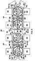
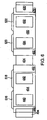
- An alternate embodiment of the invention is the clustering of two or more dual buffer chamber cluster tools, creating a multiple buffer chamber, multiple process chamber semiconductor processing tool or clustered dual buffer chamber. This embodiment is depicted in Figures 5 and 6. As such, the reader is encouraged to refer to Figures 5 and 6 simultaneously for the best understanding of the invention.
- the clustered tool 400 as shown in Figure 5, has two dual buffer chambers 402 and 406, connect by a cluster mating chamber 404.
- Dual buffer chamber 402 has a septigonal structure 408 which features sides 450 and 452 having an equal length, sides 444 and 446 having an equal length longer than the length of side 450, sides 448 and 454 having an equal length longer than side 444, and a seventh shortest side 456.
- Sides 448 and 454 are parallel to each other.
- Side 448 is bounded by side 450 and 444.
- Side 450 is also bounded by side 456.
- Side 456 is also bounded by side 452.
- Side 452 is also bounded by side 454.
- Side 454 is also bounded by side 446.
- Side 446 is also bounded by side 444.
- Two load lock chambers 432 and 434 are disposed on sides 444 and 446 respectively.
- a cluster mating chamber 404 is disposed on side 456.
- a pair of process chambers 436 and 438 are disposed on side 448.
- An access area 458 is defined by and separates chambers 436 and 438.
- a second pair of process chambers 440 and 442 are disposed on side 454.
- An access area 460 is defined by and separates process chambers 440 and 442. The access areas 458 and 460 are large enough to provide maintenance access to dual buffer chamber 402.
- buffer chambers 410 and 416 Disposed within the septigonal structure 408 are buffer chambers 410 and 416, and wafer transfer locations 412 and 414.
- the wafer transfer locations may be chambers.
- a central wall 418 runs perpendicular to sides 448 and 454 and separates buffer chambers 410 and 416.
- Wafer transfer locations 412 and 414 provide a passage through the central wall 418, with each transfer chamber 412 and 414 individually connecting buffer chambers 410 and 416.
- the wafer transfer locations 412 and 414 are selectively isolated from adjoining buffer chamber 410 and 416 by a plurality (i.e., four) slit valves 428.
- Each wafer transfer location 412 and 414, and the cluster mating chamber 404 has a pedestal 534, 536, and 538, respectively.
- Both buffer chambers 410 and 416 have an independently operable lid 516 and 518 respectively (see Figure 6) attached to septigonal structure 408 that allows access to said buffer chambers
- the buffer chamber 410 is circumscribed by the load lock chambers 432 and 434, process chambers 436 and 440, and wafer transfer locations 412 and 414.
- the load lock chambers 432 and 434, and process chambers 436 and 440 are selectively isolated from adjoining buffer chamber 410 by a plurality (i.e., four) of slit valves 424.
- Located within buffer chamber 410 is first vacuum port 526 and a first robotic wafer transport mechanism 420, e.g., a single blade robot (SBR). Other types of transfer mechanisms may be substituted.
- the first robotic wafer transport mechanism 420 shown has a wafer transport blade 422 attached to the distal ends of a pair of extendible arms 423a and 423b. The blade 422 is used by first robotic wafer transport mechanism 420 for carrying the individual wafers to and from the chambers surrounding buffer chamber 410.
- the second buffer chamber 416 is circumscribed by the process chambers 438 and 442, the cluster mating chamber 404, and wafer transfer locations 412 and 414.
- Each of the process chambers 438 and 442 are selectively isolated from adjoining buffer chamber 416 by a plurality (i.e., two) slit valves 424.
- the cluster mating chamber 404 is selectively isolated from the adjoining buffer chamber 416 by slit valve 430.
- Located within buffer chamber 416 is a second vacuum port 528 and a second robotic wafer transport mechanism 426, e.g., a single blade robot (SBR).
- the second robotic wafer transport mechanism 426 shown has a wafer transport blade 427 attached to the distal ends of a pair of extendible arms 429a and 429b. The blade 427 is used by second robotic wafer transport mechanism 426 for carrying the individual wafers to and from the chambers surrounding buffer chamber 416.
- Dual buffer chamber 406 has a septigonal structure 500 which features sides 474 and 480 having an equal length, sides 476 and 478 having an equal length shorter than 474, sides 472 and 482 having an equal length shorter than 476, and a seventh shortest side 470.
- Sides 474 and 480 are parallel.
- Side 476 is bounded by 478 on one side and side 474 on the other.
- Side 478 is also bounded by side 480.
- Side 480 also bounded by side 482.
- Side 482 is also bounded by side 470.
- Side 470 is also bounded by side 472.
- Mating chamber 404 is disposed on side 470.
- Two process chambers 488 and 490 are disposed on sides 476 and 478 respectively.
- a pair of process chambers 484 and 486 are disposed on side 474.
- An access area 466 is defined by and separates chamber process chambers 484 and 486.
- a second pair of process chambers 492 and 494 are disposed on side 480.
- An access area 468 is defined by and separates chamber process chambers 492 and 494. The access areas 466 and 468 are large enough to provide maintenance access to dual buffer chamber 406.
- buffer chambers 504 and 510 Disposed within the septigonal structure 500 are buffer chambers 504 and 510, and wafer transfer locations 496 and 498.
- a central wall 502 runs perpendicular to sides 474 and 480 and separate buffer chambers 504 and 510.
- wafer transfer locations 496 and 498 provide a passage through the central wall 502, with each transfer chamber 496 and 498 individually connecting buffer chambers 504 and 510.
- the wafer transfer locations 496 and 498 are selectively isolated from adjoining buffer chamber 504 and 510 by a plurality (i.e., four) slit valves 428.
- Each wafer transfer location 496 and 498 additionally has a pedestal 540 and 542, respectively.
- Both buffer chambers 504 and 510 having an independently operable lid 520 and 522 respectively ( Figure 6) attached to septigonal structure 500 that allows for access to chamber 504 and 510.
- the buffer chamber 504 is circumscribed by the cluster mating chamber 404, process chambers 484 and 494, and wafer transfer locations 496 and 498.
- Each of the process chambers 484 and 494 are selectively isolated from adjoining buffer chamber 504 by a plurality (i.e., two) slit valve 424.
- the cluster mating chamber 404 is selectively isolated from the buffer chamber 504 by a slit valve 430.
- Located within buffer chamber 504 is a third vacuum port 530 and a third robotic wafer transport mechanism 506, e.g., a single blade robot (SBR). Other types of transfer mechanisms may be substituted.
- SBR single blade robot
- the third robotic wafer transport mechanism 506 shown has a wafer transport blade 508 attached to the distal ends of a pair of extendible arms 507a and 507b.
- the blade 508 is used by third robotic wafer transport mechanism 506 for carrying the individual wafers to and from the chambers surrounding buffer chamber 504.
- the second buffer chamber 510 is circumscribed by the process chambers 486, 488, 490 and 492, and wafer transfer locations 496 and 498. Each process chamber 486, 488, 490 and 492 is selectively isolated from buffer chamber 510 by a plurality (i.e., four) slit valves 424. Located within buffer chamber 510 is a fourth vacuum port 532 and a fourth robotic wafer transport mechanism 512, e.g., a single blade robot (SBR). The fourth robotic wafer transport mechanism 512 shown has a wafer transport blade 514 attached to the distal ends of a pair of extendible arms 524a and 524b. The blade 514 is used by fourth robotic wafer transport mechanism 512 for carrying the individual wafers to and from the chambers surrounding buffer chamber 510.
- SBR single blade robot
- dual buffer chambers 402 and 406 illustrate the cluster mating chamber 404 positioned as to create a linear relation between the respective buffer chambers, this is illustrative only.
- the number of dual buffer chambers, process chambers per buffer chamber, geometry of the buffers and the location of the cluster mating chamber is dependent on a number of parameters unique to each user's needs, including but not limited to desired wafer throughput, available factory floor space, production line layouts and capital constraints. Many other configurations which embody the teachings of the invention will be readily apparent to those skilled in the arts.
- the vacuum ports 526, 528, 530, and 532 are connected to a pumping mechanism (not shown) such as a turbo molecular pump, which is capable of evacuating the environments of chambers 410, 416, 504 and 510, respectively.
- a pumping mechanism such as a turbo molecular pump, which is capable of evacuating the environments of chambers 410, 416, 504 and 510, respectively.
- the configuration and location of the vacuum ports may vary dependent on design criteria for individual systems, for example the use of a single port in conjunction with a high volume pump.
- the slit valves 424 and 428 isolating the buffer chamber 410 from the surrounding chambers remain closed unless wafer transfer requires access to a particular chamber.
- the slit valves 424, 428 and 430 isolating buffer chambers 416, 504 and 510 operate similarly.
- Wafer processing begins when the chambers 410, 416, 504, and 510 are pumped down to a vacuum condition by the pumping mechanism.
- the first wafer transfer robot 420 retrieves a wafer from one of the load lock chambers (e.g. 432) and carries that wafer to the first stage of processing, for example, a physical vapor deposition (PVD) in chamber 436.
- PVD physical vapor deposition
- the first robotic wafer transport mechanism 420 can either wait for the chamber 436 to become available or move the wafer to a pedestal 534 located within wafer transfer location (e.g. 412). Once the first robotic wafer transport mechanism 420 no longer is carrying a wafer, first robotic wafer transport mechanism 420 can tend wafers in the other chambers surrounding buffer chamber 410. If chamber 436 is available, the first robotic wafer transport mechanism 420 deposits the wafer in chamber 436. Once the wafer is processed and PVD stage deposits material upon the wafer, the wafer can then be moved to a second stage of processing, and so on.
- the wafer must be . transported into one of the wafer transfer locations (e.g., 412).
- the slit valve 428 isolating the wafer transfer location 412 front the buffer chamber 410 opens, allowing the wafer to be inserted into the wafer transfer location 412.
- the wafer transport blade 422 connected to first robotic wafer transport mechanism 420 is removed from wafer transport chamber 412 leaving the wafer on the pedestal 534.
- a second slit valve 428 separating the buffer chamber 416 and the transport chamber 412 is opened, allowing a wafer transport blade 427 connected to the second robotic wafer transport mechanism. 426 to be inserted into wafer transport chamber 412 to retrieve the wafer.
- the second slit valve 428 is closed and the second robotic wafer transport mechanism 426 is free to move the wafer to the desired processing chamber or sequence of chambers serviced by buffer chamber 416 and second robotic wafer transport mechanism 426.
- the wafer is then transported by second robotic wafer transport mechanism 426 to the cluster mating chamber 404 and deposited on a pedestal 538.
- a second slit valve 430 separating the buffer chamber 504 and the cluster mating chamber 404 is opened, allowing a wafer transport blade 508 connected to the third robotic wafer transport mechanism 506 to be inserted into the cluster mating chamber 404 to retrieve the wafer.
- the second slit valve 430 is closed and the third robotic wafer transport mechanism 506 is free to move the wafer to the desired processing chamber or sequence of chambers serviced by buffer chamber 504 and third robotic wafer transport mechanism 506.
- the wafer is then transported by third robotic wafer transport mechanism 506 into one of the wafer transfer location (e.g., 496).
- the wafer transport blade 508 connected to third robotic wafer transport mechanism 506 is removed from wafer transport chamber 496 leaving the wafer on the pedestal 540.
- a fourth slit valve 428 separating the buffer chamber 510 and the transport chamber 496 is opened, allowing a wafer transport blade 514 connected to the fourth robotic wafer transport mechanism 512 to be inserted into wafer transport chamber 496 to retrieve the wafer.
- the second slit valve 428 is closed and the fourth robotic wafer transport mechanism 512 is free to move the wafer to the desired processing chamber or sequence of chambers serviced by buffer chamber 510 and fourth robotic wafer transport mechanism 512.
- the wafer is loaded into a cassette (not shown) in a load lock (e.g., 434), moving back through the wafer transfer and cluster mating chambers when necessary.
- a load lock e.g., 434
- wafer processing requirements in buffer chambers to the left of wafer location may require movement to the left during over the course of wafer processing. This may be accomplished by reversing the order of the steps required to transfer the wafer through any of the transfer or cluster mating chambers as needed.
- the sequencing of the slit valves between the buffer chambers 410 416, 504, and 510, transfer chambers 412, 414, 496 and 498 and the cluster mating chamber 404 is for example only. Some slit valves remain open dependant upon desired vacuum condition in the adjoining chamber or to reduce wafer transfer time as necessary.
- the chambers 410, 416, 504 and 510 may require service. Maintenance personnel can reach the chambers 410, 416, 504 and 510 at access areas 458, 460, 466 and 468, and gain access to the interior of said chambers by opening or removing the lids 516, 518, 520 and 522.
- serial processing of wafers is facilitated by allowing a large number of process chambers to be clustered within one tool. This yields the important benefits of maintaining the wafer within a controlled environment, saving time and preventing costly damage and contamination to the wafer, minimizing tool foot-print, increasing wafer throughput by having more process chambers available within a tool and having more robots available for the increased demands of wafer transfer, and allowing the tool to share peripheral components which assist in keeping capital costs at a minimum.
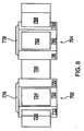
- FIG. 7 A third embodiment of the invention, a modular dual buffer chamber cluster tool 700 is shown in Figure 7 and Figure 8. As such, the reader should refer to Figures 7 and 8 simultaneously for the best understanding of the invention.
- the tool 700 has first and second modules 702 and 704, respectively, joined by a module mating chamber 706.
- the first module 702 has a septigonal chamber body 708 featuring sides 710, 712, 714 and 722 having an equal length, sides 716 and 720 having an equal length, and a seventh side 718.
- Sides 716 and 720 are shorter than the other sides.
- Side 714 is parallel to side 722 and is bordered by sides 712 and 716.
- Side 712 is also bordered by side 710.
- Side 710 is also bordered by side 722.
- Side 722 is also bordered by side 720.
- Side 720 is also bordered by side 718.
- Load lock chambers 726 and 728 are disposed on sides 710 and 712, respectively.
- Process chambers 724 and 730 are disposed on sides 722 and 714, respectively.
- the module mating chamber 706 is disposed on side 718.
- a buffer chamber 732 is centrally located within chamber body 708.
- a plurality (i.e., four) of slit valves 738 selectively isolate the buffer chamber 732 from the process chambers 730 and 724, and the load lock chambers 726 and 728.
- a slit valve 740 selectively isolates the module mating chamber 706 from buffer chamber 732.
- the module mating chamber 706 additionally has a pedestal 784.
- a first vacuum port 780 and a first robotic wafer transport mechanism 734 e.g., a single blade robot (SBR). Other types of transport mechanisms may be substituted.
- SBR single blade robot
- the first robotic wafer transport mechanism 734 shown has a wafer transport blade 736 attached to the distal ends of a pair of extendible arms 786a and 786b.
- the blade 736 is used by first robotic water transport mechanism 734 for carrying the individual wafers to and from the chambers surrounding chamber 732.
- the second module 704 has a chamber body 746 featuring sides 754, 756, 758 and 760 having an equal length, sides 748 and 752 having an equal length, and a seventh side 750.
- Side 754 is parallel to side 760.
- Sides 748 and 752 are shorter than the other sides.
- Side 754 is bordered by sides 752 and 756.
- Side 752 is also bordered by side 750.
- Side 750 is also bordered by side 748.
- Sides 748 is also bordered by 760.
- Side 760 is also bordered by side 758.
- Side 758 is also bordered by side 756.
- Process chambers 762, 764, 766 and 768 are disposed to sides 760, 754, 756 and 758 respectively.
- the module mating chamber 706 is disposed to side 750.
- a buffer chamber 770 is centrally located within chamber body 746.
- the buffer chamber 770 is circumscribed by the process chambers 762, 764, 766 and 768, and a module mating chamber 706.
- a plurality (i.e., four) of slit valves 738 isolate the buffer chamber 770 from the process chambers 762, 764, 766 and 768.
- a slit valve 740 isolates the module mating chamber 706 from buffer chamber 770.
- Located within buffer chamber 770 is a second vacuum port 782 and a second robotic wafer transport mechanism 772, e.g., a single blade robot (SBR). Other types of transport mechanisms may be substituted.
- SBR single blade robot
- the second robotic wafer transport mechanism 772 shown has a wafer transport blade 774 attached to the distal ends of a pair of extendible arms 738a and 738b.
- the blade 774 is used by second robotic wafer transport mechanism 772 for carrying the individual wafers to and from the chambers surrounding chamber 770.
- Both buffer chambers 732 and 770 have an independently operable lid 776 and 778 (see Figure 8) respectively attached to chamber bodies 708 and 746 that allow access to buffer chambers 732 and 770.
- modules 702 and 704 illustrate the cluster mating chamber 706 secured to a particular side of the modules, this is for example only.
- the particular side attached to the mating chamber 706, the number of buffer chambers, process chambers per buffer chamber, geometry of the modules and the location of the cluster mating chamber is dependent on a number of parameters unique to each user's needs, including but not limited to the wafer throughput desired, available factory floor space, production line layout and capital constraints.
- a person skilled in the art may readily use these teaching to obtain varied embodiments while remaining within the spirit of invention.
- the vacuum ports 780 and 782 are connected to a pumping mechanism (not shown) such as a turbo molecular pump, which is capable of evacuating the environments of chambers 732 and 770, respectively.
- a pumping mechanism such as a turbo molecular pump, which is capable of evacuating the environments of chambers 732 and 770, respectively.
- the configuration and location of the vacuum ports may vary dependent on design criteria for individual systems, for example the use of a single port in conjunction with a high volume pump.
- the slit valves isolating the buffer chamber 732 from the surrounding chambers remain closed unless wafer transfer requires access to a particular chamber.
- the slit valves isolating buffer chamber 770 operate similarly. Wafer processing, for example, begins when the buffer chambers 732 and 770 are pumped to a vacuum condition by the pumping mechanism.
- the first robotic wafer transport mechanism 734 retrieves a wafer from one of the load lock chambers (e.g. 728) and carries that wafer to the first stage of processing, for example, physical vapor deposition (PVD) in process chamber 730.
- PVD physical vapor deposition
- the first, robotic wafer transport mechanism 734 can either wait for the process chamber 730 to become available or move the wafer to a pedestal 784 located within the module mating chamber 706. Once the first robotic wafer transport mechanism 734 no longer is carrying a wafer, first robotic wafer transport mechanism 734 can tend wafers in the other chambers surrounding buffer chamber 732. If process chamber 730 is available, the first robotic wafer transport mechanism 734 deposits the wafer in process chamber 730. Once the wafer is processed and PVD stage deposits material upon the wafer, the wafer can then be moved to a second stage of processing, and so on.
- the wafer must be transported into the module mating chamber 706.
- the slit valve 740 isolating the buffer chamber 732 and the mating chamber 706 is opened to allow the water to enter the mating chamber 706.
- the wafer transport blade 736 connected to first robotic wafer transport mechanism 734 is removed from the module mating chamber 706 leaving the wafer on the pedestal 784.
- a second slit valve 740 separating the buffer chamber 770 and the module mating chamber 706 is opened, allowing a wafer transport blade 774 connected to the second robotic wafer transport mechanism 772 to be inserted into the module mating chamber 706 to retrieve the wafer.
- the second slit valve 740 is closed and the second robotic wafer transport mechanism 772 is free to move the wafer to the desired processing chamber or sequence of chambers serviced by buffer chamber 770 and second robotic wafer transport, mechanism 772.
- the wafer is loaded into a cassette (not shown) in a load lock (e.g., 726), moving back through the module mating chamber 706 when necessary.
- a load lock e.g., 726
- the buffer chambers 732 and 770 may require service. Maintenance personnel can reach the buffer chambers 732 and 770 at service locations 742 and 744, and gain access to the interior of buffer chambers 732 and 770 by opening or removing the lids 776 and 778.
- the robots can directly access the pedestals within the transfer and mating chambers. The direct access increases the speed of wafer transfer and throughput while allowing for a more cost effective and smaller tool.
- Tool 900 has a septigonal chamber body 902 which features a pair of equal length sides 910 and 916, a second pair of equal length sides 912 and 914, a third pair of equal length sides 904 and 908, and a seventh side 906.
- Side 914 is bounded by 916 on one side and side 912 on the other.
- Side 916 is also bounded by side 904.
- Sides 910 and 916 are parallel to each other and are the longer than sides 904, 906 and 912.
- Side 910 is bounded by sides 908 and 912. Sides 904 and 908 are shorter than side 912, and are separated by side 906.
- Two load lock chambers 940 and 942 are disposed on sides 912 and 914 respectively.
- a set of process chambers 930 and 932 are disposed on side 916.
- a second set of process chambers 936 and 938 are disposed on side 910.
- a first and second buffer chamber 922 and 928 Disposed within the septigonal chamber body 902 are a first and second buffer chamber 922 and 928, respectively, and wafer transfer locations 924 and 926, respectively.
- the wafer transfer locations may be a chamber.
- a central wall 920 runs perpendicularly from side 910 to side 916 and separates buffer chambers 922 and 928.
- Wafer transfer locations 924 and 926 provide a passage through the central wall 920, each chamber 924 and 926 individually connects buffer chambers 922 and 928, creating a single environment 972.
- Each wafer transfer location 924 and 926 has a pedestal 968 and 970, respectively.
- Both buffer chambers 922 and 928 have an independent lid 960 and 962 respectively (see Figure 10).
- Access areas 946 and 948 are defined by process chambers 930 and 932 along side 916 and by process chamber 936 and 938 along side 910 and provide access to the buffer chambers 922 and 928.
- the first buffer chamber 922 is circumscribed by the load lock chambers 940 and 942, process chambers 930 and 938, and wafer transfer locations 924 and 926.
- the load lock chambers 940 and 942, and process chambers 930 and 938 are selectively isolated from adjoining buffer chamber 922 by a plurality (i.e., four) slit valves 958.
- Located within buffer chamber 922 is a first vacuum port 962 and a first robotic wafer transport mechanism 950, e.g., a single blade robot (SBR). Other types of transfer mechanisms may be substituted.
- the first robotic wafer transport mechanism 950 shown has a wafer transport blade 952 attached to the distal ends of a pair of extendible arms 960a and 960b. The blade 952 is used by first robotic wafer transport mechanism 950 for carrying the individual wafers to and from the chambers surrounding buffer chamber 922.
- a second buffer chamber 928 is circumscribed by the process chambers 932, 934 and 936, and wafer transfer locations 924 and 926.
- the process chambers 932, 934 and 936 are selectively isolated from adjoining buffer chamber 928 by a plurality (i.e., four) slit valves 958.
- Located within second buffer chamber 928 is a second vacuum port 964 and a second robotic wafer transport mechanism 954, e.g., a single blade robot (SBR).
- the second robotic wafer transport mechanism 954 shown has a wafer transport blade 956 attached to the distal ends of a pair of extendible arms 966a and 966b. The blade 956 is used by second robotic wafer transport mechanism 954 for carrying the individual wafers to and from the chambers surrounding buffer chamber 928.
- the configuration of the tool 900 is shown having seven sides, it is noted that a six-sided structure may be desired in certain applications where the sides 904, 906 and 908 are replaced with two sides equal in length to side 912. This will allow an additional process chamber to be added to the tool.
- Many other configurations in addition to the one described above which embody the teachings of the invention will be readily apparent to those skilled in the arts.
- the vacuum ports 962 and 964 are connected to a pumping mechanism (not shown) such as a turbo molecular pump, which is capable of evacuating the environments of chambers 922 and 928, respectively.
- a pumping mechanism such as a turbo molecular pump, which is capable of evacuating the environments of chambers 922 and 928, respectively.
- the configuration and location of the vacuum ports may vary dependent on design criteria for individual systems, for example the use of a single port in conjunction with a high volume pump.
- the slit valves 958 isolating the buffer chamber 922 from the surrounding process chambers 930 and 938, and load lock chambers 940 and 942 remain closed unless wafer transfer requires access to those particular chambers.
- the slit valves 958 isolating buffer chamber 928 operate similarly to isolate process chambers 932, 934 and 936.
- Wafer processing begins when the chamber 922 and 928 are pumped to a vacuum condition by the pumping mechanism.
- the first robotic wafer transport mechanism 950 retrieves a wafer from one of the load lock chambers (e.g., 942) and carries that wafer to the first stage of processing, for example, physical vapor deposition (PVD) in chamber 930.
- PVD physical vapor deposition
- the first robotic wafer transport mechanism 950 can either wait for the chamber 930 to become available or move the wafer to a pedestal 968 located within wafer transfer location (e.g., 924). Once the first robotic wafer transport mechanism 950 no longer is carrying a wafer, first robotic wafer transport mechanism 950 can tend wafers in the other chambers surrounding buffer chamber 922. If chamber 930 is available, the first robotic wafer transport mechanism 950 deposits the wafer in chamber 930. Once the wafer is processed and PVD stage deposits material upon the wafer, the wafer can then be moved to a second stage of processing, and so on.
- the wafer must be transported into one of the wafer transfer location (e.g., 924).
- the wafer transport blade 952 connected to first robotic wafer transport mechanism 950 is removed from wafer transport chamber 924 leaving the wafer on the pedestal 968.
- Wafer transport blade 956 connected to the second robotic wafer transport mechanism 954 to be inserted into wafer transport chamber 924 to retrieve the wafer.
- the second robotic wafer transport mechanism 954 is free to move the wafer to the desired processing chamber or sequence of chambers serviced by buffer chamber 928 and second robotic wafer transport mechanism 954.
- the wafer is loaded into a cassette (not shown) in a load lock (e.g., 940), moving back through the wafer transfer locations when necessary.
- a load lock e.g. 940
- wafer processing requirements may require additional wafer transfer between buffer chambers during the course of wafer processing.
- the chambers 922 and 928 may require service. Maintenance personnel can reach the chambers 922 and 928 at access areas 946 and 948, and gain access to the interior of chambers 922 and 928 by opening or removing the lids 960 and 962
- the present invention saves significant time by facilitating wafer transport between robotic wafer transport mechanisms without having to wait for the opening and closing of slit valves and environmental changes to occur within a transfer chamber. Additionally, the elimination of the slit valves allows the non-isolated tool 900 disclosed in Figure 9 to enjoy the cost savings associated with fewer components and simpler operation as compared to prior art processing tools.
- An embodiment which maximizes the ability to reduce further the foot-print and costs savings of the non-isolated dual buffer chamber cluster tool is a "squeezed" non-isolated dual buffer chamber, multiple process chamber semiconductor processing tool or “squeezed” dual buffer chamber cluster tool.
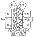
- the “squeezed” tool is depicted in Figures 11 and 12. As such, the reader should refer to Figures 11 and 12 simultaneously for the best understanding of the invention.
- the "squeezed" tool 1100 referring primarily to Figure 11 has octagonal chamber body 1130 which features sides 1140 and 1146 having an equal length, sides 1142 and 1144 having an equal length shorter than side 1140, sides 1134 and 1136 having an equal length shorter than side 1142, and sides 1132 and 1138 having an equal length shorter than side 1134.
- Sides 1140 and 1146 are parallel to each.
- Side 1140 is bounded by 1136 and side 1142.
- Side 1142 is also bounded by side 1144.
- Side 1144 is also bounded by 1146.
- Side 1146 is also bounded by side 1132.
- Side 1132 is also bounded by 1134.
- Side 1134 is also bounded by side 1136.
- a buffer chamber 1116 Disposed within the octagonal chamber body 1130 is a buffer chamber 1116.
- the environment 1172 of buffer chamber 1116 is selectively isolated from adjoining load locks and process chambers by a plurality (i.e., eight) of slit valves 1162.
- Buffer chamber 1116 additionally has a singular lid 1150 (see Figure 12).
- Disposed within the buffer chamber 1116 are a first robotic wafer transport mechanism 1118, a second robotic wafer transport mechanism 1120, a vacuum port 1164, and a first and second pedestal 1122 and 1124, respectively.
- the vacuum port connects the buffer chamber 1116 to a pumping mechanism (not shown) such as a turbo molecular pump.
- the first robotic wafer transport mechanism 1118 is for example, a single blade robot (SBR). Other types of transport mechanism may be substituted.
- the first robotic wafer transport mechanism 1118 shown has a wafer transport blade 1166 attached to the distal ends of a pair of extendible arms, 1168a and 1168b.
- the pedestals 1122 and 1124 are located along an imaginary axis 1160 which bisects sides 1140 and 1146.
- Two load lock chambers 1112 and 1114 are attached to sides 1136 and 1134, respectively.
- a set of process chambers 1101 and 1102 are disposed on side 1140 and define an access area 1176.
- a second set of process chambers 1108 and 1110 are disposed on side 1146 and define an access area 1178.
- Access area 1176 and 1178 may be eliminated if a minimized foot-print is desired.
- Process chambers 1104 and 1106 are disposed on sides 1142 and 1144, respectively.
- the first robotic wafer transport mechanism 1118 is substantially centrally located to the load lock chambers 1112 and 1114, process chambers 1101 and 1110 and the pedestals 1122 and 1124.
- First robotic wafer transport mechanism 1118 is additionally equidistant from pedestals 1122 and 1124.
- the blade 1166 is used by first robotic wafer transport mechanism 1118 to facilitate transfer of wafers among the load lock chambers 1112 and 1114, process chambers 1101 and 11101 and the pedestals 1122 and 1124.
- the second robotic wafer transport mechanism 1120 is for example, a single blade robot (SBR). Other types of transport mechanism may be substituted.
- the second robotic wafer transport mechanism 1120 shown has a wafer transport blade 1170 attached to the distal ends of a pair of extendible arms, 1172a and 1172b.
- the second robotic wafer transport mechanism 1120 is substantially centrally located to the process chambers 1102, 1104, 1106 and 1108 and the pedestals 1122 and 1124.
- Second robotic wafer transport mechanism 1120 is additionally equidistant from pedestals 1122 and 1124.
- the blade 1166 is used by second robotic wafer transport mechanism 1120 to facilitate transfer of wafers among process chambers 1102, 1104, 1106 and 1108, and the pedestals 1122 and 1124.
- the vacuum port 1164 is connected to a pumping mechanism (not shown) such as a turbo molecular pump, which is capable of evacuating the environment of buffer chamber 1116.
- a pumping mechanism such as a turbo molecular pump
- the configuration and location of the vacuum ports may vary dependent on design criteria for individual systems, for example the use of a single port in conjunction with a high volume pump.
- the slit valves isolating the buffer chamber 1116 from the surrounding process chambers (1101, 1102, 1104, 1106, 1108, 1110) and load lock chambers (1112, 1114) chambers remain closed unless wafer transfer requires access to those particular chambers.
- Wafer processing begins when the buffer chamber 1116 is pumped down to a vacuum condition by the pumping mechanism.
- the first robotic wafer transfer mechanism 1118 retrieves a wafer from one of the load lock chambers (e.g. 1112) and carries that wafer to the first stage of processing, for example, physical vapor deposition (PVD) in chamber 1101. If the chamber is occupied, the first robotic transfer mechanism 1118 can either wait for the chamber 1101 to become available or move the wafer to a pedestal 1122.
- PVD physical vapor deposition
- first robotic transfer mechanism 1118 can tend wafers in the other chambers and platforms serviced by first robotic transfer mechanism 1118. If chamber 1101 is available, the first robotic transfer mechanism 1118 deposits the wafer in chamber 1101. Once the wafer is processed and PVD stage deposits material upon the wafer, the wafer can then be moved to a second stage of processing, and so on.
- Second robotic transfer mechanism 1120 retrieves the wafer from pedestal 1122 and delivers the wafer to the desired processing chamber or sequence of chambers serviced by second robotic transfer mechanism 1120.
- the wafer is loaded into a cassette (not shown) in a load lock (e.g., 1114), moving back across the pedestals when necessary.
- a load lock e.g., 1114
- wafer processing requirements may require additional wafer transfer across the pedestals during the course of wafer processing.
- the present invention saves significant time by facilitating wafer transport between robotic mechanisms without having to wait for the opening and closing of slit valves and environmental changes to occur when using a transfer chamber. Additionally, the elimination of the transfer chambers and the use of a singular lid 1150 allow the "squeezed" tool 1100 disclosed in Figure 11 to enjoy a reduced foot-print and the cost savings associated with fewer components and simpler operation as compared to the other embodiments.
Landscapes
- Container, Conveyance, Adherence, Positioning, Of Wafer (AREA)
- Drying Of Semiconductors (AREA)
Abstract
Description
Claims (16)
- A semiconductor workpiece processing apparatus (300) comprising:at least one polygonal structure (344) having a plurality of sides;at least one of said sides having at least two process chambers disposed thereupon, defining an access area to said polygonal structure between said process chambers.
- The apparatus of claim 1 further comprising:a first buffer chamber (346) disposed in said at least one polygonal structure, anda second buffer chamber (350) disposed in said at least one polygonal structure.
- The apparatus according to any one of the preceding claims further comprising:at least one wafer transfer location (314, 316) disposed within said polygonal structure.
- The apparatus of claim 3 wherein said wafer transfer location is a chamber.
- The apparatus according to any one of claims 2 to 4, wherein said first and second buffer chambers (346, 350) further comprise:a first (354) and a second (356) lid disposed above said first (346) and second (350) buffer chambers, respectively, thereby defining a single environment within said first and second buffer chambers.
- The apparatus according to any one of claims 2 to 4, wherein said first (346) and second (350) buffer chambers further comprise:a plurality of slit valves (322) disposed about and selectively isolating said first and second buffer chamber, anda first and a second lid (354, 356) disposed above said first and second buffer chambers, respectively, thereby defining a first and second environment within said first and second buffer chambers, respectively.
- A semiconductor workpiece processing apparatus (400) comprising:a first polygonal module (402) having a plurality of sides,at least a second polygonal module (406) having a plurality of sides, andat least one mating chamber (404) for connecting said first and said at least second polygonal modules.
- The apparatus of claim 7 wherein said first and said at least second polygonal modules each further comprise:a first and a second process chamber disposed on at least one side of said first and at least said second polygonal modules defining an access area.
- The apparatus of any one of claims 7 and 8 further comprising:at least one buffer chamber disposed within said first polygonal module.
- The apparatus of claim 9 wherein said at least one buffer chamber is:a first buffer chamber and a second buffer chamber.
- The apparatus of any one of claims 7 to 10 further comprising:at least one wafer transfer location disposed within said at least one mating chamber.
- The apparatus of any one of claims 10 and 11, wherein said first and second buffer chambers further comprise:a plurality of slit valves creating a first and a second environment within said first and said second buffer chamber, respectfully.
- A semiconductor workpiece processing apparatus comprising:at least one polygonal structure having a plurality of sides;a buffer chamber disposed within said at least one polygonal structure;a lid disposed above said at least one polygonal structure thereby defining a single environment within said buffer chamber; andat least two wafer transfer mechanisms disposed within said buffer chamber.
- The apparatus of claim 13 further comprising:at least six slit valves disposed within said buffer chamber.
- The apparatus of any one of claims 13 and 14 further comprising:a first and a second process chamber disposed on one of said sides defining an access area between said first and said second process chambers and said one side.
- The apparatus of any one of claims 13 to 15 further comprising a single vacuum port.
Applications Claiming Priority (2)
| Application Number | Priority Date | Filing Date | Title |
|---|---|---|---|
| US318233 | 1981-11-04 | ||
| US09/318,233 US6440261B1 (en) | 1999-05-25 | 1999-05-25 | Dual buffer chamber cluster tool for semiconductor wafer processing |
Publications (2)
| Publication Number | Publication Date |
|---|---|
| EP1056123A2 true EP1056123A2 (en) | 2000-11-29 |
| EP1056123A3 EP1056123A3 (en) | 2001-04-18 |
Family
ID=23237282
Family Applications (1)
| Application Number | Title | Priority Date | Filing Date |
|---|---|---|---|
| EP00111298A Withdrawn EP1056123A3 (en) | 1999-05-25 | 2000-05-25 | Dual buffer chamber cluster tool for semiconductor wafer processing |
Country Status (3)
| Country | Link |
|---|---|
| US (1) | US6440261B1 (en) |
| EP (1) | EP1056123A3 (en) |
| JP (1) | JP2001135705A (en) |
Cited By (1)
| Publication number | Priority date | Publication date | Assignee | Title |
|---|---|---|---|---|
| WO2003017354A1 (en) * | 2001-08-14 | 2003-02-27 | Tokyo Electron Limited | Semiconductor processing system |
Families Citing this family (374)
| Publication number | Priority date | Publication date | Assignee | Title |
|---|---|---|---|---|
| TW504941B (en) * | 1999-07-23 | 2002-10-01 | Semiconductor Energy Lab | Method of fabricating an EL display device, and apparatus for forming a thin film |
| JP4644926B2 (en) * | 2000-10-13 | 2011-03-09 | ソニー株式会社 | Semiconductor manufacturing apparatus and semiconductor device manufacturing method |
| US6962471B2 (en) * | 2000-10-26 | 2005-11-08 | Leica Microsystems Jena Gmbh | Substrate conveying module and system made up of substrate conveying module and workstation |
| US6852194B2 (en) * | 2001-05-21 | 2005-02-08 | Tokyo Electron Limited | Processing apparatus, transferring apparatus and transferring method |
| JP2003060005A (en) * | 2001-08-20 | 2003-02-28 | Ulvac Japan Ltd | Vacuum processing equipment |
| JP4821074B2 (en) * | 2001-08-31 | 2011-11-24 | 東京エレクトロン株式会社 | Processing system |
| US6604853B2 (en) * | 2001-10-11 | 2003-08-12 | Taiwan Semiconductor Manufacturing Co., Ltd | Accelerated thermal stress cycle test |
| CN100423179C (en) * | 2002-06-21 | 2008-10-01 | 应用材料股份有限公司 | Transfer chambers for vacuum processing systems |
| KR100490702B1 (en) * | 2002-11-21 | 2005-05-19 | 주성엔지니어링(주) | Multi cluster module |
| KR101077630B1 (en) * | 2003-01-02 | 2011-10-27 | 로마 린다 유니버시티 메디칼 센터 | Configuration management and retrieval system for proton beam therapy system |
| DE10350517A1 (en) * | 2003-10-29 | 2005-06-09 | Sieghard Schiller Gmbh & Co. Kg | Holder for semiconductor wafer stack has robotic handling arm and separate stacks rotatable about a vertical axis for free access and transportation |
| KR100578134B1 (en) * | 2003-11-10 | 2006-05-10 | 삼성전자주식회사 | Multi-chamber system |
| US8029226B2 (en) * | 2003-11-10 | 2011-10-04 | Brooks Automation, Inc. | Semiconductor manufacturing systems |
| US8812150B2 (en) * | 2003-11-10 | 2014-08-19 | Brooks Automation, Inc. | Semiconductor manufacturing process modules |
| US20070269297A1 (en) * | 2003-11-10 | 2007-11-22 | Meulen Peter V D | Semiconductor wafer handling and transport |
| US10086511B2 (en) | 2003-11-10 | 2018-10-02 | Brooks Automation, Inc. | Semiconductor manufacturing systems |
| US7458763B2 (en) | 2003-11-10 | 2008-12-02 | Blueshift Technologies, Inc. | Mid-entry load lock for semiconductor handling system |
| US8313277B2 (en) | 2003-11-10 | 2012-11-20 | Brooks Automation, Inc. | Semiconductor manufacturing process modules |
| US20050223837A1 (en) | 2003-11-10 | 2005-10-13 | Blueshift Technologies, Inc. | Methods and systems for driving robotic components of a semiconductor handling system |
| US8696298B2 (en) * | 2003-11-10 | 2014-04-15 | Brooks Automation, Inc. | Semiconductor manufacturing process modules |
| US8403613B2 (en) * | 2003-11-10 | 2013-03-26 | Brooks Automation, Inc. | Bypass thermal adjuster for vacuum semiconductor processing |
| TWD107408S1 (en) * | 2004-05-28 | 2005-11-01 | 東京威力科創股份有限公司 | Transmission Processing Room |
| CN101866828B (en) * | 2004-06-02 | 2013-03-20 | 应用材料公司 | Electron device manufacturing chamber and forming method thereof |
| US20060201074A1 (en) * | 2004-06-02 | 2006-09-14 | Shinichi Kurita | Electronic device manufacturing chamber and methods of forming the same |
| US7784164B2 (en) * | 2004-06-02 | 2010-08-31 | Applied Materials, Inc. | Electronic device manufacturing chamber method |
| WO2006004718A1 (en) * | 2004-06-28 | 2006-01-12 | Brooks Automation, Inc. | Non productive wafer buffer module for substrate processing apparatus |
| US20060137609A1 (en) * | 2004-09-13 | 2006-06-29 | Puchacz Jerzy P | Multi-single wafer processing apparatus |
| US20070020890A1 (en) * | 2005-07-19 | 2007-01-25 | Applied Materials, Inc. | Method and apparatus for semiconductor processing |
| KR100803726B1 (en) * | 2005-08-12 | 2008-02-15 | 주식회사 아이피에스 | Structure of the conveying chamber |
| TWI342058B (en) * | 2005-12-20 | 2011-05-11 | Applied Materials Inc | Extended mainframe designs for semiconductor device manufacturing equipment |
| JP2009533876A (en) * | 2006-04-11 | 2009-09-17 | アプライド マテリアルズ インコーポレイテッド | System configuration and method for forming solar cell panels |
| WO2008011579A2 (en) * | 2006-07-21 | 2008-01-24 | Aixtron, Inc. | Small volume symmetric flow single wafer ald apparatus |
| KR100847888B1 (en) * | 2006-12-12 | 2008-07-23 | 세메스 주식회사 | Semiconductor device manufacturing apparatus |
| US20080276867A1 (en) | 2007-05-09 | 2008-11-13 | Jason Schaller | Transfer chamber with vacuum extension for shutter disks |
| WO2008149446A1 (en) * | 2007-06-07 | 2008-12-11 | Canon Anelva Corporation | Semiconductor production apparatus and process |
| US20100012036A1 (en) * | 2008-07-11 | 2010-01-21 | Hugo Silva | Isolation for multi-single-wafer processing apparatus |
| US9394608B2 (en) | 2009-04-06 | 2016-07-19 | Asm America, Inc. | Semiconductor processing reactor and components thereof |
| US20100304027A1 (en) * | 2009-05-27 | 2010-12-02 | Applied Materials, Inc. | Substrate processing system and methods thereof |
| US8802201B2 (en) | 2009-08-14 | 2014-08-12 | Asm America, Inc. | Systems and methods for thin-film deposition of metal oxides using excited nitrogen-oxygen species |
| WO2011156650A2 (en) | 2010-06-10 | 2011-12-15 | Applied Materials, Inc. | Low resistivity tungsten pvd with enhanced ionization and rf power coupling |
| JP2012028659A (en) * | 2010-07-27 | 2012-02-09 | Hitachi High-Technologies Corp | Vacuum processing apparatus |
| WO2012098871A1 (en) * | 2011-01-20 | 2012-07-26 | 東京エレクトロン株式会社 | Vacuum processing apparatus |
| US20130023129A1 (en) | 2011-07-20 | 2013-01-24 | Asm America, Inc. | Pressure transmitter for a semiconductor processing environment |
| US9017481B1 (en) | 2011-10-28 | 2015-04-28 | Asm America, Inc. | Process feed management for semiconductor substrate processing |
| DE102012103295A1 (en) | 2012-01-09 | 2013-07-11 | Aixtron Se | Device useful for coating semiconductor substrates, comprises processing unit, which is centrally arranged transfer module, loading- or unloading interface, power modules comprising a gas mixing system, pipelines, and a service space |
| TWI725303B (en) * | 2012-02-10 | 2021-04-21 | 美商布魯克斯自動機械公司 | Substrate processing apparatus |
| US20140001576A1 (en) | 2012-06-27 | 2014-01-02 | Applied Materials, Inc. | Lowering tungsten resistivity by replacing titanium nitride with titanium silicon nitride |
| US10714315B2 (en) | 2012-10-12 | 2020-07-14 | Asm Ip Holdings B.V. | Semiconductor reaction chamber showerhead |
| US20160376700A1 (en) | 2013-02-01 | 2016-12-29 | Asm Ip Holding B.V. | System for treatment of deposition reactor |
| WO2014163791A1 (en) * | 2013-03-12 | 2014-10-09 | Applied Materials, Inc | Semiconductor device manufacturing platform with single and twinned processing chambers |
| DE102013111790A1 (en) | 2013-10-25 | 2015-04-30 | Aixtron Se | Energy and material consumption optimized CVD reactor |
| DE102013113052A1 (en) | 2013-11-26 | 2015-05-28 | Aixtron Se | Heating device for a CVD reactor |
| US11015245B2 (en) | 2014-03-19 | 2021-05-25 | Asm Ip Holding B.V. | Gas-phase reactor and system having exhaust plenum and components thereof |
| US10858737B2 (en) | 2014-07-28 | 2020-12-08 | Asm Ip Holding B.V. | Showerhead assembly and components thereof |
| US9890456B2 (en) | 2014-08-21 | 2018-02-13 | Asm Ip Holding B.V. | Method and system for in situ formation of gas-phase compounds |
| US10941490B2 (en) | 2014-10-07 | 2021-03-09 | Asm Ip Holding B.V. | Multiple temperature range susceptor, assembly, reactor and system including the susceptor, and methods of using the same |
| US10276355B2 (en) | 2015-03-12 | 2019-04-30 | Asm Ip Holding B.V. | Multi-zone reactor, system including the reactor, and method of using the same |
| US10458018B2 (en) | 2015-06-26 | 2019-10-29 | Asm Ip Holding B.V. | Structures including metal carbide material, devices including the structures, and methods of forming same |
| US10014196B2 (en) * | 2015-10-20 | 2018-07-03 | Lam Research Corporation | Wafer transport assembly with integrated buffers |
| US10211308B2 (en) | 2015-10-21 | 2019-02-19 | Asm Ip Holding B.V. | NbMC layers |
| US11139308B2 (en) | 2015-12-29 | 2021-10-05 | Asm Ip Holding B.V. | Atomic layer deposition of III-V compounds to form V-NAND devices |
| US10529554B2 (en) | 2016-02-19 | 2020-01-07 | Asm Ip Holding B.V. | Method for forming silicon nitride film selectively on sidewalls or flat surfaces of trenches |
| US10343920B2 (en) | 2016-03-18 | 2019-07-09 | Asm Ip Holding B.V. | Aligned carbon nanotubes |
| US10190213B2 (en) | 2016-04-21 | 2019-01-29 | Asm Ip Holding B.V. | Deposition of metal borides |
| US10865475B2 (en) | 2016-04-21 | 2020-12-15 | Asm Ip Holding B.V. | Deposition of metal borides and silicides |
| US10367080B2 (en) | 2016-05-02 | 2019-07-30 | Asm Ip Holding B.V. | Method of forming a germanium oxynitride film |
| US11453943B2 (en) | 2016-05-25 | 2022-09-27 | Asm Ip Holding B.V. | Method for forming carbon-containing silicon/metal oxide or nitride film by ALD using silicon precursor and hydrocarbon precursor |
| US9859151B1 (en) | 2016-07-08 | 2018-01-02 | Asm Ip Holding B.V. | Selective film deposition method to form air gaps |
| US10612137B2 (en) | 2016-07-08 | 2020-04-07 | Asm Ip Holdings B.V. | Organic reactants for atomic layer deposition |
| US9812320B1 (en) | 2016-07-28 | 2017-11-07 | Asm Ip Holding B.V. | Method and apparatus for filling a gap |
| KR102532607B1 (en) | 2016-07-28 | 2023-05-15 | 에이에스엠 아이피 홀딩 비.브이. | Substrate processing apparatus and method of operating the same |
| US9887082B1 (en) | 2016-07-28 | 2018-02-06 | Asm Ip Holding B.V. | Method and apparatus for filling a gap |
| US10643826B2 (en) | 2016-10-26 | 2020-05-05 | Asm Ip Holdings B.V. | Methods for thermally calibrating reaction chambers |
| US11532757B2 (en) | 2016-10-27 | 2022-12-20 | Asm Ip Holding B.V. | Deposition of charge trapping layers |
| US10229833B2 (en) | 2016-11-01 | 2019-03-12 | Asm Ip Holding B.V. | Methods for forming a transition metal nitride film on a substrate by atomic layer deposition and related semiconductor device structures |
| US10714350B2 (en) | 2016-11-01 | 2020-07-14 | ASM IP Holdings, B.V. | Methods for forming a transition metal niobium nitride film on a substrate by atomic layer deposition and related semiconductor device structures |
| KR102546317B1 (en) | 2016-11-15 | 2023-06-21 | 에이에스엠 아이피 홀딩 비.브이. | Gas supply unit and substrate processing apparatus including the same |
| KR102762543B1 (en) | 2016-12-14 | 2025-02-05 | 에이에스엠 아이피 홀딩 비.브이. | Substrate processing apparatus |
| US11447861B2 (en) | 2016-12-15 | 2022-09-20 | Asm Ip Holding B.V. | Sequential infiltration synthesis apparatus and a method of forming a patterned structure |
| US11581186B2 (en) | 2016-12-15 | 2023-02-14 | Asm Ip Holding B.V. | Sequential infiltration synthesis apparatus |
| KR102700194B1 (en) * | 2016-12-19 | 2024-08-28 | 에이에스엠 아이피 홀딩 비.브이. | Substrate processing apparatus |
| US10269558B2 (en) | 2016-12-22 | 2019-04-23 | Asm Ip Holding B.V. | Method of forming a structure on a substrate |
| US10867788B2 (en) | 2016-12-28 | 2020-12-15 | Asm Ip Holding B.V. | Method of forming a structure on a substrate |
| US11390950B2 (en) | 2017-01-10 | 2022-07-19 | Asm Ip Holding B.V. | Reactor system and method to reduce residue buildup during a film deposition process |
| US10468261B2 (en) | 2017-02-15 | 2019-11-05 | Asm Ip Holding B.V. | Methods for forming a metallic film on a substrate by cyclical deposition and related semiconductor device structures |
| US10529563B2 (en) | 2017-03-29 | 2020-01-07 | Asm Ip Holdings B.V. | Method for forming doped metal oxide films on a substrate by cyclical deposition and related semiconductor device structures |
| KR102457289B1 (en) | 2017-04-25 | 2022-10-21 | 에이에스엠 아이피 홀딩 비.브이. | Method for depositing a thin film and manufacturing a semiconductor device |
| US10770286B2 (en) | 2017-05-08 | 2020-09-08 | Asm Ip Holdings B.V. | Methods for selectively forming a silicon nitride film on a substrate and related semiconductor device structures |
| US10892156B2 (en) | 2017-05-08 | 2021-01-12 | Asm Ip Holding B.V. | Methods for forming a silicon nitride film on a substrate and related semiconductor device structures |
| US10886123B2 (en) | 2017-06-02 | 2021-01-05 | Asm Ip Holding B.V. | Methods for forming low temperature semiconductor layers and related semiconductor device structures |
| US10043693B1 (en) | 2017-06-06 | 2018-08-07 | Applied Materials, Inc. | Method and apparatus for handling substrates in a processing system having a buffer chamber |
| US12040200B2 (en) | 2017-06-20 | 2024-07-16 | Asm Ip Holding B.V. | Semiconductor processing apparatus and methods for calibrating a semiconductor processing apparatus |
| US11306395B2 (en) | 2017-06-28 | 2022-04-19 | Asm Ip Holding B.V. | Methods for depositing a transition metal nitride film on a substrate by atomic layer deposition and related deposition apparatus |
| TWI794238B (en) | 2017-07-13 | 2023-03-01 | 荷蘭商Asm智慧財產控股公司 | Apparatus and method for removal of oxide and carbon from semiconductor films in a single processing chamber |
| KR20190009245A (en) | 2017-07-18 | 2019-01-28 | 에이에스엠 아이피 홀딩 비.브이. | Methods for forming a semiconductor device structure and related semiconductor device structures |
| US11018002B2 (en) | 2017-07-19 | 2021-05-25 | Asm Ip Holding B.V. | Method for selectively depositing a Group IV semiconductor and related semiconductor device structures |
| US11374112B2 (en) | 2017-07-19 | 2022-06-28 | Asm Ip Holding B.V. | Method for depositing a group IV semiconductor and related semiconductor device structures |
| US10541333B2 (en) | 2017-07-19 | 2020-01-21 | Asm Ip Holding B.V. | Method for depositing a group IV semiconductor and related semiconductor device structures |
| US10590535B2 (en) | 2017-07-26 | 2020-03-17 | Asm Ip Holdings B.V. | Chemical treatment, deposition and/or infiltration apparatus and method for using the same |
| TWI815813B (en) | 2017-08-04 | 2023-09-21 | 荷蘭商Asm智慧財產控股公司 | Showerhead assembly for distributing a gas within a reaction chamber |
| US10692741B2 (en) | 2017-08-08 | 2020-06-23 | Asm Ip Holdings B.V. | Radiation shield |
| US10770336B2 (en) | 2017-08-08 | 2020-09-08 | Asm Ip Holding B.V. | Substrate lift mechanism and reactor including same |
| US11139191B2 (en) | 2017-08-09 | 2021-10-05 | Asm Ip Holding B.V. | Storage apparatus for storing cassettes for substrates and processing apparatus equipped therewith |
| US11769682B2 (en) | 2017-08-09 | 2023-09-26 | Asm Ip Holding B.V. | Storage apparatus for storing cassettes for substrates and processing apparatus equipped therewith |
| US11830730B2 (en) | 2017-08-29 | 2023-11-28 | Asm Ip Holding B.V. | Layer forming method and apparatus |
| KR102491945B1 (en) | 2017-08-30 | 2023-01-26 | 에이에스엠 아이피 홀딩 비.브이. | Substrate processing apparatus |
| US11056344B2 (en) | 2017-08-30 | 2021-07-06 | Asm Ip Holding B.V. | Layer forming method |
| US11295980B2 (en) | 2017-08-30 | 2022-04-05 | Asm Ip Holding B.V. | Methods for depositing a molybdenum metal film over a dielectric surface of a substrate by a cyclical deposition process and related semiconductor device structures |
| KR102401446B1 (en) | 2017-08-31 | 2022-05-24 | 에이에스엠 아이피 홀딩 비.브이. | Substrate processing apparatus |
| KR102630301B1 (en) | 2017-09-21 | 2024-01-29 | 에이에스엠 아이피 홀딩 비.브이. | Method of sequential infiltration synthesis treatment of infiltrateable material and structures and devices formed using same |
| US10844484B2 (en) | 2017-09-22 | 2020-11-24 | Asm Ip Holding B.V. | Apparatus for dispensing a vapor phase reactant to a reaction chamber and related methods |
| US10658205B2 (en) | 2017-09-28 | 2020-05-19 | Asm Ip Holdings B.V. | Chemical dispensing apparatus and methods for dispensing a chemical to a reaction chamber |
| US10403504B2 (en) | 2017-10-05 | 2019-09-03 | Asm Ip Holding B.V. | Method for selectively depositing a metallic film on a substrate |
| US10923344B2 (en) | 2017-10-30 | 2021-02-16 | Asm Ip Holding B.V. | Methods for forming a semiconductor structure and related semiconductor structures |
| US10910262B2 (en) | 2017-11-16 | 2021-02-02 | Asm Ip Holding B.V. | Method of selectively depositing a capping layer structure on a semiconductor device structure |
| US11022879B2 (en) | 2017-11-24 | 2021-06-01 | Asm Ip Holding B.V. | Method of forming an enhanced unexposed photoresist layer |
| TWI791689B (en) | 2017-11-27 | 2023-02-11 | 荷蘭商Asm智慧財產控股私人有限公司 | Apparatus including a clean mini environment |
| WO2019103613A1 (en) | 2017-11-27 | 2019-05-31 | Asm Ip Holding B.V. | A storage device for storing wafer cassettes for use with a batch furnace |
| US10872771B2 (en) | 2018-01-16 | 2020-12-22 | Asm Ip Holding B. V. | Method for depositing a material film on a substrate within a reaction chamber by a cyclical deposition process and related device structures |
| US11482412B2 (en) | 2018-01-19 | 2022-10-25 | Asm Ip Holding B.V. | Method for depositing a gap-fill layer by plasma-assisted deposition |
| TWI799494B (en) | 2018-01-19 | 2023-04-21 | 荷蘭商Asm 智慧財產控股公司 | Deposition method |
| US11018047B2 (en) | 2018-01-25 | 2021-05-25 | Asm Ip Holding B.V. | Hybrid lift pin |
| USD880437S1 (en) | 2018-02-01 | 2020-04-07 | Asm Ip Holding B.V. | Gas supply plate for semiconductor manufacturing apparatus |
| US11081345B2 (en) | 2018-02-06 | 2021-08-03 | Asm Ip Holding B.V. | Method of post-deposition treatment for silicon oxide film |
| US10896820B2 (en) | 2018-02-14 | 2021-01-19 | Asm Ip Holding B.V. | Method for depositing a ruthenium-containing film on a substrate by a cyclical deposition process |
| WO2019158960A1 (en) | 2018-02-14 | 2019-08-22 | Asm Ip Holding B.V. | A method for depositing a ruthenium-containing film on a substrate by a cyclical deposition process |
| US10731249B2 (en) | 2018-02-15 | 2020-08-04 | Asm Ip Holding B.V. | Method of forming a transition metal containing film on a substrate by a cyclical deposition process, a method for supplying a transition metal halide compound to a reaction chamber, and related vapor deposition apparatus |
| KR102636427B1 (en) | 2018-02-20 | 2024-02-13 | 에이에스엠 아이피 홀딩 비.브이. | Substrate processing method and apparatus |
| US10975470B2 (en) | 2018-02-23 | 2021-04-13 | Asm Ip Holding B.V. | Apparatus for detecting or monitoring for a chemical precursor in a high temperature environment |
| US11473195B2 (en) | 2018-03-01 | 2022-10-18 | Asm Ip Holding B.V. | Semiconductor processing apparatus and a method for processing a substrate |
| US11629406B2 (en) | 2018-03-09 | 2023-04-18 | Asm Ip Holding B.V. | Semiconductor processing apparatus comprising one or more pyrometers for measuring a temperature of a substrate during transfer of the substrate |
| US11114283B2 (en) | 2018-03-16 | 2021-09-07 | Asm Ip Holding B.V. | Reactor, system including the reactor, and methods of manufacturing and using same |
| KR102646467B1 (en) | 2018-03-27 | 2024-03-11 | 에이에스엠 아이피 홀딩 비.브이. | Method of forming an electrode on a substrate and a semiconductor device structure including an electrode |
| US11230766B2 (en) | 2018-03-29 | 2022-01-25 | Asm Ip Holding B.V. | Substrate processing apparatus and method |
| US11088002B2 (en) | 2018-03-29 | 2021-08-10 | Asm Ip Holding B.V. | Substrate rack and a substrate processing system and method |
| KR102501472B1 (en) | 2018-03-30 | 2023-02-20 | 에이에스엠 아이피 홀딩 비.브이. | Substrate processing method |
| KR102600229B1 (en) | 2018-04-09 | 2023-11-10 | 에이에스엠 아이피 홀딩 비.브이. | Substrate supporting device, substrate processing apparatus including the same and substrate processing method |
| TWI843623B (en) | 2018-05-08 | 2024-05-21 | 荷蘭商Asm Ip私人控股有限公司 | Methods for depositing an oxide film on a substrate by a cyclical deposition process and related device structures |
| US12025484B2 (en) | 2018-05-08 | 2024-07-02 | Asm Ip Holding B.V. | Thin film forming method |
| US12272527B2 (en) | 2018-05-09 | 2025-04-08 | Asm Ip Holding B.V. | Apparatus for use with hydrogen radicals and method of using same |
| KR20190129718A (en) | 2018-05-11 | 2019-11-20 | 에이에스엠 아이피 홀딩 비.브이. | Methods for forming a doped metal carbide film on a substrate and related semiconductor device structures |
| KR102596988B1 (en) | 2018-05-28 | 2023-10-31 | 에이에스엠 아이피 홀딩 비.브이. | Method of processing a substrate and a device manufactured by the same |
| TWI840362B (en) | 2018-06-04 | 2024-05-01 | 荷蘭商Asm Ip私人控股有限公司 | Wafer handling chamber with moisture reduction |
| US11718913B2 (en) | 2018-06-04 | 2023-08-08 | Asm Ip Holding B.V. | Gas distribution system and reactor system including same |
| US11286562B2 (en) | 2018-06-08 | 2022-03-29 | Asm Ip Holding B.V. | Gas-phase chemical reactor and method of using same |
| KR102568797B1 (en) | 2018-06-21 | 2023-08-21 | 에이에스엠 아이피 홀딩 비.브이. | Substrate processing system |
| US10797133B2 (en) | 2018-06-21 | 2020-10-06 | Asm Ip Holding B.V. | Method for depositing a phosphorus doped silicon arsenide film and related semiconductor device structures |
| WO2020003000A1 (en) | 2018-06-27 | 2020-01-02 | Asm Ip Holding B.V. | Cyclic deposition methods for forming metal-containing material and films and structures including the metal-containing material |
| KR20250134000A (en) | 2018-06-27 | 2025-09-09 | 에이에스엠 아이피 홀딩 비.브이. | Cyclic deposition methods for forming metal-containing material and films and structures including the metal-containing material |
| US10612136B2 (en) | 2018-06-29 | 2020-04-07 | ASM IP Holding, B.V. | Temperature-controlled flange and reactor system including same |
| KR102686758B1 (en) | 2018-06-29 | 2024-07-18 | 에이에스엠 아이피 홀딩 비.브이. | Method for depositing a thin film and manufacturing a semiconductor device |
| US10755922B2 (en) | 2018-07-03 | 2020-08-25 | Asm Ip Holding B.V. | Method for depositing silicon-free carbon-containing film as gap-fill layer by pulse plasma-assisted deposition |
| US10388513B1 (en) | 2018-07-03 | 2019-08-20 | Asm Ip Holding B.V. | Method for depositing silicon-free carbon-containing film as gap-fill layer by pulse plasma-assisted deposition |
| US10767789B2 (en) | 2018-07-16 | 2020-09-08 | Asm Ip Holding B.V. | Diaphragm valves, valve components, and methods for forming valve components |
| US11053591B2 (en) | 2018-08-06 | 2021-07-06 | Asm Ip Holding B.V. | Multi-port gas injection system and reactor system including same |
| US10883175B2 (en) | 2018-08-09 | 2021-01-05 | Asm Ip Holding B.V. | Vertical furnace for processing substrates and a liner for use therein |
| US10829852B2 (en) | 2018-08-16 | 2020-11-10 | Asm Ip Holding B.V. | Gas distribution device for a wafer processing apparatus |
| US11430674B2 (en) | 2018-08-22 | 2022-08-30 | Asm Ip Holding B.V. | Sensor array, apparatus for dispensing a vapor phase reactant to a reaction chamber and related methods |
| KR102707956B1 (en) | 2018-09-11 | 2024-09-19 | 에이에스엠 아이피 홀딩 비.브이. | Method for deposition of a thin film |
| US11024523B2 (en) | 2018-09-11 | 2021-06-01 | Asm Ip Holding B.V. | Substrate processing apparatus and method |
| US11049751B2 (en) | 2018-09-14 | 2021-06-29 | Asm Ip Holding B.V. | Cassette supply system to store and handle cassettes and processing apparatus equipped therewith |
| CN110970344B (en) | 2018-10-01 | 2024-10-25 | Asmip控股有限公司 | Substrate holding device, system including the same and method of using the same |
| US11232963B2 (en) | 2018-10-03 | 2022-01-25 | Asm Ip Holding B.V. | Substrate processing apparatus and method |
| KR102592699B1 (en) | 2018-10-08 | 2023-10-23 | 에이에스엠 아이피 홀딩 비.브이. | Substrate support unit and apparatuses for depositing thin film and processing the substrate including the same |
| KR102546322B1 (en) | 2018-10-19 | 2023-06-21 | 에이에스엠 아이피 홀딩 비.브이. | Substrate processing apparatus and substrate processing method |
| KR102605121B1 (en) | 2018-10-19 | 2023-11-23 | 에이에스엠 아이피 홀딩 비.브이. | Substrate processing apparatus and substrate processing method |
| USD948463S1 (en) | 2018-10-24 | 2022-04-12 | Asm Ip Holding B.V. | Susceptor for semiconductor substrate supporting apparatus |
| US12378665B2 (en) | 2018-10-26 | 2025-08-05 | Asm Ip Holding B.V. | High temperature coatings for a preclean and etch apparatus and related methods |
| US11087997B2 (en) | 2018-10-31 | 2021-08-10 | Asm Ip Holding B.V. | Substrate processing apparatus for processing substrates |
| KR102748291B1 (en) | 2018-11-02 | 2024-12-31 | 에이에스엠 아이피 홀딩 비.브이. | Substrate support unit and substrate processing apparatus including the same |
| US11572620B2 (en) | 2018-11-06 | 2023-02-07 | Asm Ip Holding B.V. | Methods for selectively depositing an amorphous silicon film on a substrate |
| US11031242B2 (en) | 2018-11-07 | 2021-06-08 | Asm Ip Holding B.V. | Methods for depositing a boron doped silicon germanium film |
| US10818758B2 (en) | 2018-11-16 | 2020-10-27 | Asm Ip Holding B.V. | Methods for forming a metal silicate film on a substrate in a reaction chamber and related semiconductor device structures |
| US10847366B2 (en) | 2018-11-16 | 2020-11-24 | Asm Ip Holding B.V. | Methods for depositing a transition metal chalcogenide film on a substrate by a cyclical deposition process |
| US12040199B2 (en) | 2018-11-28 | 2024-07-16 | Asm Ip Holding B.V. | Substrate processing apparatus for processing substrates |
| US11217444B2 (en) | 2018-11-30 | 2022-01-04 | Asm Ip Holding B.V. | Method for forming an ultraviolet radiation responsive metal oxide-containing film |
| KR102636428B1 (en) | 2018-12-04 | 2024-02-13 | 에이에스엠 아이피 홀딩 비.브이. | A method for cleaning a substrate processing apparatus |
| US11158513B2 (en) | 2018-12-13 | 2021-10-26 | Asm Ip Holding B.V. | Methods for forming a rhenium-containing film on a substrate by a cyclical deposition process and related semiconductor device structures |
| JP7504584B2 (en) | 2018-12-14 | 2024-06-24 | エーエスエム・アイピー・ホールディング・ベー・フェー | Method and system for forming device structures using selective deposition of gallium nitride - Patents.com |
| TWI866480B (en) | 2019-01-17 | 2024-12-11 | 荷蘭商Asm Ip 私人控股有限公司 | Methods of forming a transition metal containing film on a substrate by a cyclical deposition process |
| KR102727227B1 (en) | 2019-01-22 | 2024-11-07 | 에이에스엠 아이피 홀딩 비.브이. | Semiconductor processing device |
| CN111524788B (en) | 2019-02-01 | 2023-11-24 | Asm Ip私人控股有限公司 | Method for forming topologically selective films of silicon oxide |
| TWI838458B (en) | 2019-02-20 | 2024-04-11 | 荷蘭商Asm Ip私人控股有限公司 | Apparatus and methods for plug fill deposition in 3-d nand applications |
| KR102626263B1 (en) | 2019-02-20 | 2024-01-16 | 에이에스엠 아이피 홀딩 비.브이. | Cyclical deposition method including treatment step and apparatus for same |
| TWI845607B (en) | 2019-02-20 | 2024-06-21 | 荷蘭商Asm Ip私人控股有限公司 | Cyclical deposition method and apparatus for filling a recess formed within a substrate surface |
| KR102638425B1 (en) | 2019-02-20 | 2024-02-21 | 에이에스엠 아이피 홀딩 비.브이. | Method and apparatus for filling a recess formed within a substrate surface |
| TWI842826B (en) | 2019-02-22 | 2024-05-21 | 荷蘭商Asm Ip私人控股有限公司 | Substrate processing apparatus and method for processing substrate |
| KR102782593B1 (en) | 2019-03-08 | 2025-03-14 | 에이에스엠 아이피 홀딩 비.브이. | Structure Including SiOC Layer and Method of Forming Same |
| US11742198B2 (en) | 2019-03-08 | 2023-08-29 | Asm Ip Holding B.V. | Structure including SiOCN layer and method of forming same |
| KR102858005B1 (en) | 2019-03-08 | 2025-09-09 | 에이에스엠 아이피 홀딩 비.브이. | Method for Selective Deposition of Silicon Nitride Layer and Structure Including Selectively-Deposited Silicon Nitride Layer |
| JP2020167398A (en) | 2019-03-28 | 2020-10-08 | エーエスエム・アイピー・ホールディング・ベー・フェー | Door openers and substrate processing equipment provided with door openers |
| KR102809999B1 (en) | 2019-04-01 | 2025-05-19 | 에이에스엠 아이피 홀딩 비.브이. | Method of manufacturing semiconductor device |
| KR102897355B1 (en) | 2019-04-19 | 2025-12-08 | 에이에스엠 아이피 홀딩 비.브이. | Layer forming method and apparatus |
| KR20200125453A (en) | 2019-04-24 | 2020-11-04 | 에이에스엠 아이피 홀딩 비.브이. | Gas-phase reactor system and method of using same |
| KR102869364B1 (en) | 2019-05-07 | 2025-10-10 | 에이에스엠 아이피 홀딩 비.브이. | Method for Reforming Amorphous Carbon Polymer Film |
| KR102929471B1 (en) | 2019-05-07 | 2026-02-20 | 에이에스엠 아이피 홀딩 비.브이. | Chemical source vessel with dip tube |
| KR102929472B1 (en) | 2019-05-10 | 2026-02-20 | 에이에스엠 아이피 홀딩 비.브이. | Method of depositing material onto a surface and structure formed according to the method |
| JP7612342B2 (en) | 2019-05-16 | 2025-01-14 | エーエスエム・アイピー・ホールディング・ベー・フェー | Wafer boat handling apparatus, vertical batch furnace and method |
| JP7598201B2 (en) | 2019-05-16 | 2024-12-11 | エーエスエム・アイピー・ホールディング・ベー・フェー | Wafer boat handling apparatus, vertical batch furnace and method |
| USD975665S1 (en) | 2019-05-17 | 2023-01-17 | Asm Ip Holding B.V. | Susceptor shaft |
| USD947913S1 (en) | 2019-05-17 | 2022-04-05 | Asm Ip Holding B.V. | Susceptor shaft |
| USD935572S1 (en) | 2019-05-24 | 2021-11-09 | Asm Ip Holding B.V. | Gas channel plate |
| US10998209B2 (en) | 2019-05-31 | 2021-05-04 | Applied Materials, Inc. | Substrate processing platforms including multiple processing chambers |
| USD922229S1 (en) | 2019-06-05 | 2021-06-15 | Asm Ip Holding B.V. | Device for controlling a temperature of a gas supply unit |
| KR20200141003A (en) | 2019-06-06 | 2020-12-17 | 에이에스엠 아이피 홀딩 비.브이. | Gas-phase reactor system including a gas detector |
| KR102918757B1 (en) | 2019-06-10 | 2026-01-28 | 에이에스엠 아이피 홀딩 비.브이. | Method for cleaning quartz epitaxial chambers |
| KR20200143254A (en) | 2019-06-11 | 2020-12-23 | 에이에스엠 아이피 홀딩 비.브이. | Method of forming an electronic structure using an reforming gas, system for performing the method, and structure formed using the method |
| USD944946S1 (en) | 2019-06-14 | 2022-03-01 | Asm Ip Holding B.V. | Shower plate |
| USD931978S1 (en) | 2019-06-27 | 2021-09-28 | Asm Ip Holding B.V. | Showerhead vacuum transport |
| KR102911421B1 (en) | 2019-07-03 | 2026-01-12 | 에이에스엠 아이피 홀딩 비.브이. | Temperature control assembly for substrate processing apparatus and method of using same |
| JP7316121B2 (en) * | 2019-07-05 | 2023-07-27 | 東京エレクトロン株式会社 | Substrate transfer device and substrate transfer method |
| JP7499079B2 (en) | 2019-07-09 | 2024-06-13 | エーエスエム・アイピー・ホールディング・ベー・フェー | Plasma device using coaxial waveguide and substrate processing method |
| CN112216646B (en) | 2019-07-10 | 2026-02-10 | Asmip私人控股有限公司 | Substrate support assembly and substrate processing apparatus including the thereof |
| KR102895115B1 (en) | 2019-07-16 | 2025-12-03 | 에이에스엠 아이피 홀딩 비.브이. | Substrate processing apparatus |
| KR102955799B1 (en) | 2019-07-17 | 2026-04-21 | 에이에스엠 아이피 홀딩 비.브이. | Radical assist ignition plasma system and method |
| KR102860110B1 (en) | 2019-07-17 | 2025-09-16 | 에이에스엠 아이피 홀딩 비.브이. | Methods of forming silicon germanium structures |
| US11643724B2 (en) | 2019-07-18 | 2023-05-09 | Asm Ip Holding B.V. | Method of forming structures using a neutral beam |
| KR102903090B1 (en) | 2019-07-19 | 2025-12-19 | 에이에스엠 아이피 홀딩 비.브이. | Method of Forming Topology-Controlled Amorphous Carbon Polymer Film |
| TWI839544B (en) | 2019-07-19 | 2024-04-21 | 荷蘭商Asm Ip私人控股有限公司 | Method of forming topology-controlled amorphous carbon polymer film |
| TWI851767B (en) | 2019-07-29 | 2024-08-11 | 荷蘭商Asm Ip私人控股有限公司 | Methods for selective deposition utilizing n-type dopants and/or alternative dopants to achieve high dopant incorporation |
| JP7240980B2 (en) * | 2019-07-29 | 2023-03-16 | 東京エレクトロン株式会社 | SUBSTRATE PROCESSING APPARATUS AND SUBSTRATE CONVEYING METHOD |
| CN112309899B (en) | 2019-07-30 | 2025-11-14 | Asmip私人控股有限公司 | Substrate processing equipment |
| CN112309900B (en) | 2019-07-30 | 2025-11-04 | Asmip私人控股有限公司 | Substrate processing equipment |
| KR102971074B1 (en) | 2019-07-30 | 2026-05-29 | 에이에스엠 아이피 홀딩 비.브이. | Substrate processing apparatus and method |
| US12622218B2 (en) | 2019-07-31 | 2026-05-05 | Asm Ip Holding B.V. | Cassette lid opening device |
| US11587815B2 (en) | 2019-07-31 | 2023-02-21 | Asm Ip Holding B.V. | Vertical batch furnace assembly |
| US11587814B2 (en) | 2019-07-31 | 2023-02-21 | Asm Ip Holding B.V. | Vertical batch furnace assembly |
| US11227782B2 (en) | 2019-07-31 | 2022-01-18 | Asm Ip Holding B.V. | Vertical batch furnace assembly |
| CN112323048B (en) | 2019-08-05 | 2024-02-09 | Asm Ip私人控股有限公司 | Liquid level sensor for chemical source container |
| CN112342526A (en) | 2019-08-09 | 2021-02-09 | Asm Ip私人控股有限公司 | Heater assembly including cooling device and method of using same |
| USD965044S1 (en) | 2019-08-19 | 2022-09-27 | Asm Ip Holding B.V. | Susceptor shaft |
| USD965524S1 (en) | 2019-08-19 | 2022-10-04 | Asm Ip Holding B.V. | Susceptor support |
| JP7810514B2 (en) | 2019-08-21 | 2026-02-03 | エーエスエム・アイピー・ホールディング・ベー・フェー | Film-forming raw material mixed gas generating device and film-forming device |
| USD940837S1 (en) | 2019-08-22 | 2022-01-11 | Asm Ip Holding B.V. | Electrode |
| USD979506S1 (en) | 2019-08-22 | 2023-02-28 | Asm Ip Holding B.V. | Insulator |
| USD949319S1 (en) | 2019-08-22 | 2022-04-19 | Asm Ip Holding B.V. | Exhaust duct |
| KR102983146B1 (en) | 2019-08-22 | 2026-06-26 | 에이에스엠 아이피 홀딩 비.브이. | Method for forming a structure with a hole |
| USD930782S1 (en) | 2019-08-22 | 2021-09-14 | Asm Ip Holding B.V. | Gas distributor |
| KR102928101B1 (en) | 2019-08-23 | 2026-02-13 | 에이에스엠 아이피 홀딩 비.브이. | Method for depositing silicon oxide film having improved quality by peald using bis(diethylamino)silane |
| US11286558B2 (en) | 2019-08-23 | 2022-03-29 | Asm Ip Holding B.V. | Methods for depositing a molybdenum nitride film on a surface of a substrate by a cyclical deposition process and related semiconductor device structures including a molybdenum nitride film |
| CN112442674A (en) | 2019-09-03 | 2021-03-05 | Asm Ip私人控股有限公司 | Method and apparatus for depositing chalcogenide films and structures including films |
| KR102806450B1 (en) | 2019-09-04 | 2025-05-12 | 에이에스엠 아이피 홀딩 비.브이. | Methods for selective deposition using a sacrificial capping layer |
| KR102733104B1 (en) | 2019-09-05 | 2024-11-22 | 에이에스엠 아이피 홀딩 비.브이. | Substrate processing apparatus |
| US12469693B2 (en) | 2019-09-17 | 2025-11-11 | Asm Ip Holding B.V. | Method of forming a carbon-containing layer and structure including the layer |
| US11562901B2 (en) | 2019-09-25 | 2023-01-24 | Asm Ip Holding B.V. | Substrate processing method |
| CN112593212B (en) | 2019-10-02 | 2023-12-22 | Asm Ip私人控股有限公司 | Method for forming topologically selective silicon oxide film through cyclic plasma enhanced deposition process |
| TWI925822B (en) | 2019-10-08 | 2026-05-21 | 荷蘭商Asm Ip私人控股有限公司 | Gas injection system, reactor system, and method of depositing material on surface of substratewithin reaction chamber |
| KR102948143B1 (en) | 2019-10-08 | 2026-04-07 | 에이에스엠 아이피 홀딩 비.브이. | Reactor system including a gas distribution assembly for use with activated species and method of using same |
| TWI846953B (en) | 2019-10-08 | 2024-07-01 | 荷蘭商Asm Ip私人控股有限公司 | Substrate processing device |
| KR102879443B1 (en) | 2019-10-10 | 2025-11-03 | 에이에스엠 아이피 홀딩 비.브이. | Method of forming a photoresist underlayer and structure including same |
| US12009241B2 (en) | 2019-10-14 | 2024-06-11 | Asm Ip Holding B.V. | Vertical batch furnace assembly with detector to detect cassette |
| TWI834919B (en) | 2019-10-16 | 2024-03-11 | 荷蘭商Asm Ip私人控股有限公司 | Method of topology-selective film formation of silicon oxide |
| US11637014B2 (en) | 2019-10-17 | 2023-04-25 | Asm Ip Holding B.V. | Methods for selective deposition of doped semiconductor material |
| KR102845724B1 (en) | 2019-10-21 | 2025-08-13 | 에이에스엠 아이피 홀딩 비.브이. | Apparatus and methods for selectively etching films |
| KR102960940B1 (en) | 2019-10-25 | 2026-05-04 | 에이에스엠 아이피 홀딩 비.브이. | Methods for filling a gap feature on a substrate surface and related semiconductor structures |
| US11646205B2 (en) | 2019-10-29 | 2023-05-09 | Asm Ip Holding B.V. | Methods of selectively forming n-type doped material on a surface, systems for selectively forming n-type doped material, and structures formed using same |
| KR102890638B1 (en) | 2019-11-05 | 2025-11-25 | 에이에스엠 아이피 홀딩 비.브이. | Structures with doped semiconductor layers and methods and systems for forming same |
| US11501968B2 (en) | 2019-11-15 | 2022-11-15 | Asm Ip Holding B.V. | Method for providing a semiconductor device with silicon filled gaps |
| KR102861314B1 (en) | 2019-11-20 | 2025-09-17 | 에이에스엠 아이피 홀딩 비.브이. | Method of depositing carbon-containing material on a surface of a substrate, structure formed using the method, and system for forming the structure |
| CN112951697B (en) | 2019-11-26 | 2025-07-29 | Asmip私人控股有限公司 | Substrate processing apparatus |
| KR20210065848A (en) | 2019-11-26 | 2021-06-04 | 에이에스엠 아이피 홀딩 비.브이. | Methods for selectivley forming a target film on a substrate comprising a first dielectric surface and a second metallic surface |
| CN120998766A (en) | 2019-11-29 | 2025-11-21 | Asm Ip私人控股有限公司 | Substrate processing equipment |
| CN120432376A (en) | 2019-11-29 | 2025-08-05 | Asm Ip私人控股有限公司 | Substrate processing equipment |
| JP7527928B2 (en) | 2019-12-02 | 2024-08-05 | エーエスエム・アイピー・ホールディング・ベー・フェー | Substrate processing apparatus and substrate processing method |
| KR20210070898A (en) | 2019-12-04 | 2021-06-15 | 에이에스엠 아이피 홀딩 비.브이. | Substrate processing apparatus |
| CN112992667A (en) | 2019-12-17 | 2021-06-18 | Asm Ip私人控股有限公司 | Method of forming vanadium nitride layer and structure including vanadium nitride layer |
| KR102943768B1 (en) | 2019-12-19 | 2026-03-26 | 에이에스엠 아이피 홀딩 비.브이. | Methods for filling a gap feature on a substrate and related semiconductor structures |
| KR102974179B1 (en) | 2020-01-06 | 2026-06-05 | 에이에스엠 아이피 홀딩 비.브이. | Channeled lift pin |
| TWI901623B (en) | 2020-01-06 | 2025-10-21 | 荷蘭商Asm Ip私人控股有限公司 | Gas supply assembly and valve plate assembly |
| US11993847B2 (en) | 2020-01-08 | 2024-05-28 | Asm Ip Holding B.V. | Injector |
| KR102882467B1 (en) | 2020-01-16 | 2025-11-05 | 에이에스엠 아이피 홀딩 비.브이. | Method of forming high aspect ratio features |
| KR102675856B1 (en) | 2020-01-20 | 2024-06-17 | 에이에스엠 아이피 홀딩 비.브이. | Method of forming thin film and method of modifying surface of thin film |
| TWI889744B (en) | 2020-01-29 | 2025-07-11 | 荷蘭商Asm Ip私人控股有限公司 | Contaminant trap system, and baffle plate stack |
| TWI871421B (en) | 2020-02-03 | 2025-02-01 | 荷蘭商Asm Ip私人控股有限公司 | Devices and structures including a vanadium or indium layer and methods and systems for forming the same |
| KR20210100010A (en) | 2020-02-04 | 2021-08-13 | 에이에스엠 아이피 홀딩 비.브이. | Method and apparatus for transmittance measurements of large articles |
| US11776846B2 (en) | 2020-02-07 | 2023-10-03 | Asm Ip Holding B.V. | Methods for depositing gap filling fluids and related systems and devices |
| KR102916725B1 (en) | 2020-02-13 | 2026-01-23 | 에이에스엠 아이피 홀딩 비.브이. | Substrate processing apparatus including light receiving device and calibration method of light receiving device |
| TWI915339B (en) | 2020-02-13 | 2026-02-21 | 荷蘭商Asm Ip私人控股有限公司 | Gas distribution assembly, shower plate assembly, and method of adjusting conductance of gas to reaction chamber |
| TWI855223B (en) | 2020-02-17 | 2024-09-11 | 荷蘭商Asm Ip私人控股有限公司 | Method for growing phosphorous-doped silicon layer |
| TWI895326B (en) | 2020-02-28 | 2025-09-01 | 荷蘭商Asm Ip私人控股有限公司 | System dedicated for parts cleaning |
| TWI914330B (en) | 2020-03-04 | 2026-02-11 | 荷蘭商Asm Ip私人控股有限公司 | Reactor system, and alignment fixture |
| US11876356B2 (en) | 2020-03-11 | 2024-01-16 | Asm Ip Holding B.V. | Lockout tagout assembly and system and method of using same |
| KR20210116240A (en) | 2020-03-11 | 2021-09-27 | 에이에스엠 아이피 홀딩 비.브이. | Substrate handling device with adjustable joints |
| KR102775390B1 (en) | 2020-03-12 | 2025-02-28 | 에이에스엠 아이피 홀딩 비.브이. | Method for Fabricating Layer Structure Having Target Topological Profile |
| US12173404B2 (en) | 2020-03-17 | 2024-12-24 | Asm Ip Holding B.V. | Method of depositing epitaxial material, structure formed using the method, and system for performing the method |
| KR102755229B1 (en) | 2020-04-02 | 2025-01-14 | 에이에스엠 아이피 홀딩 비.브이. | Thin film forming method |
| TWI887376B (en) | 2020-04-03 | 2025-06-21 | 荷蘭商Asm Ip私人控股有限公司 | Method for manufacturing semiconductor device |
| TWI888525B (en) | 2020-04-08 | 2025-07-01 | 荷蘭商Asm Ip私人控股有限公司 | Apparatus and methods for selectively etching silcon oxide films |
| US11821078B2 (en) | 2020-04-15 | 2023-11-21 | Asm Ip Holding B.V. | Method for forming precoat film and method for forming silicon-containing film |
| KR102970066B1 (en) | 2020-04-15 | 2026-05-28 | 에이에스엠 아이피 홀딩 비.브이. | Method of forming chromium nitride layer and structure including the chromium nitride layer |
| US11996289B2 (en) | 2020-04-16 | 2024-05-28 | Asm Ip Holding B.V. | Methods of forming structures including silicon germanium and silicon layers, devices formed using the methods, and systems for performing the methods |
| TW202143328A (en) | 2020-04-21 | 2021-11-16 | 荷蘭商Asm Ip私人控股有限公司 | Method for adjusting a film stress |
| KR20210132600A (en) | 2020-04-24 | 2021-11-04 | 에이에스엠 아이피 홀딩 비.브이. | Methods and systems for depositing a layer comprising vanadium, nitrogen, and a further element |
| TWI921332B (en) | 2020-04-24 | 2026-04-11 | 荷蘭商Asm Ip私人控股有限公司 | Methods of forming structures including vanadium boride and vanadium phosphide layers, structures and devices formed thereby, and systems for manufacturing the devices |
| TWI913262B (en) | 2020-04-24 | 2026-02-01 | 荷蘭商Asm Ip私人控股有限公司 | Vertical batch furnace assembly, and method for cooling vertical batch furnace |
| JP7816915B2 (en) | 2020-04-24 | 2026-02-18 | エーエスエム・アイピー・ホールディング・ベー・フェー | Method for forming a vanadium nitride-containing layer and structures including a vanadium nitride-containing layer |
| TWI887400B (en) | 2020-04-24 | 2025-06-21 | 荷蘭商Asm Ip私人控股有限公司 | Methods and apparatus for stabilizing vanadium compounds |
| KR102783898B1 (en) | 2020-04-29 | 2025-03-18 | 에이에스엠 아이피 홀딩 비.브이. | Solid source precursor vessel |
| KR20210134869A (en) | 2020-05-01 | 2021-11-11 | 에이에스엠 아이피 홀딩 비.브이. | Fast FOUP swapping with a FOUP handler |
| TWI907417B (en) | 2020-05-04 | 2025-12-11 | 荷蘭商Asm Ip私人控股有限公司 | Semiconductor processing system |
| KR20210137395A (en) | 2020-05-07 | 2021-11-17 | 에이에스엠 아이피 홀딩 비.브이. | Apparatus and methods for performing an in-situ etch of reaction chambers with fluorine-based radicals |
| JP7736446B2 (en) | 2020-05-07 | 2025-09-09 | エーエスエム・アイピー・ホールディング・ベー・フェー | Reactor system with tuned circuit |
| TWI867219B (en) * | 2020-05-12 | 2024-12-21 | 荷蘭商Asm Ip私人控股有限公司 | Semiconductor processing system |
| KR102788543B1 (en) | 2020-05-13 | 2025-03-27 | 에이에스엠 아이피 홀딩 비.브이. | Laser alignment fixture for a reactor system |
| TWI915365B (en) | 2020-05-15 | 2026-02-21 | 荷蘭商Asm Ip私人控股有限公司 | Method of forming a silicon germanium layer, semiconductor structure, semiconductor device, method of forming a deposition layer, and deposition system |
| TW202614152A (en) | 2020-05-19 | 2026-04-01 | 荷蘭商Asm Ip私人控股有限公司 | Substrate processing apparatus |
| KR20210145079A (en) | 2020-05-21 | 2021-12-01 | 에이에스엠 아이피 홀딩 비.브이. | Flange and apparatus for processing substrates |
| KR102795476B1 (en) | 2020-05-21 | 2025-04-11 | 에이에스엠 아이피 홀딩 비.브이. | Structures including multiple carbon layers and methods of forming and using same |
| TWI873343B (en) | 2020-05-22 | 2025-02-21 | 荷蘭商Asm Ip私人控股有限公司 | Reaction system for forming thin film on substrate |
| KR20210146802A (en) | 2020-05-26 | 2021-12-06 | 에이에스엠 아이피 홀딩 비.브이. | Method for depositing boron and gallium containing silicon germanium layers |
| TWI876048B (en) | 2020-05-29 | 2025-03-11 | 荷蘭商Asm Ip私人控股有限公司 | Substrate processing device |
| US12660553B2 (en) | 2020-06-01 | 2026-06-16 | Applied Materials, Inc. | High temperature and vacuum isolation processing mini-environments |
| TW202212620A (en) | 2020-06-02 | 2022-04-01 | 荷蘭商Asm Ip私人控股有限公司 | Apparatus for processing substrate, method of forming film, and method of controlling apparatus for processing substrate |
| TW202618032A (en) | 2020-06-16 | 2026-05-01 | 荷蘭商Asm Ip私人控股有限公司 | Methods and systems for epitaxially growing boron doped silicon germanium layers and field effect transistors including the same |
| TWI908816B (en) | 2020-06-24 | 2025-12-21 | 荷蘭商Asm Ip私人控股有限公司 | Method for forming a layer provided with silicon |
| TWI873359B (en) | 2020-06-30 | 2025-02-21 | 荷蘭商Asm Ip私人控股有限公司 | Substrate processing method |
| US12431354B2 (en) | 2020-07-01 | 2025-09-30 | Asm Ip Holding B.V. | Silicon nitride and silicon oxide deposition methods using fluorine inhibitor |
| US12080571B2 (en) | 2020-07-08 | 2024-09-03 | Applied Materials, Inc. | Substrate processing module and method of moving a workpiece |
| TW202202649A (en) | 2020-07-08 | 2022-01-16 | 荷蘭商Asm Ip私人控股有限公司 | Substrate processing method |
| KR20220010438A (en) | 2020-07-17 | 2022-01-25 | 에이에스엠 아이피 홀딩 비.브이. | Structures and methods for use in photolithography |
| TWI878570B (en) | 2020-07-20 | 2025-04-01 | 荷蘭商Asm Ip私人控股有限公司 | Method and system for depositing molybdenum layers |
| KR20220011092A (en) | 2020-07-20 | 2022-01-27 | 에이에스엠 아이피 홀딩 비.브이. | Method and system for forming structures including transition metal layers |
| US12322591B2 (en) | 2020-07-27 | 2025-06-03 | Asm Ip Holding B.V. | Thin film deposition process |
| US11749542B2 (en) | 2020-07-27 | 2023-09-05 | Applied Materials, Inc. | Apparatus, system, and method for non-contact temperature monitoring of substrate supports |
| US11817331B2 (en) | 2020-07-27 | 2023-11-14 | Applied Materials, Inc. | Substrate holder replacement with protective disk during pasting process |
| KR20220020210A (en) | 2020-08-11 | 2022-02-18 | 에이에스엠 아이피 홀딩 비.브이. | Methods for Depositing a Titinum Aluminun Carbide Film Structuru on a Substrate and Releated Semiconductor Structures |
| KR102915124B1 (en) | 2020-08-14 | 2026-01-19 | 에이에스엠 아이피 홀딩 비.브이. | Method for processing a substrate |
| US12040177B2 (en) | 2020-08-18 | 2024-07-16 | Asm Ip Holding B.V. | Methods for forming a laminate film by cyclical plasma-enhanced deposition processes |
| TWI911263B (en) | 2020-08-25 | 2026-01-11 | 荷蘭商Asm Ip私人控股有限公司 | Method for cleaning a substrate, method for selectively depositing, and reaction system |
| US11725280B2 (en) | 2020-08-26 | 2023-08-15 | Asm Ip Holding B.V. | Method for forming metal silicon oxide and metal silicon oxynitride layers |
| TWI911265B (en) | 2020-08-27 | 2026-01-11 | 荷蘭商Asm Ip私人控股有限公司 | Method of forming patterned structures, method of manipulating mechanical property, and device structure |
| US11600507B2 (en) | 2020-09-09 | 2023-03-07 | Applied Materials, Inc. | Pedestal assembly for a substrate processing chamber |
| TWI904232B (en) | 2020-09-10 | 2025-11-11 | 荷蘭商Asm Ip私人控股有限公司 | Methods for depositing gap filing fluids and related systems and devices |
| USD990534S1 (en) | 2020-09-11 | 2023-06-27 | Asm Ip Holding B.V. | Weighted lift pin |
| KR20220036866A (en) | 2020-09-16 | 2022-03-23 | 에이에스엠 아이피 홀딩 비.브이. | Silicon oxide deposition method |
| US11610799B2 (en) | 2020-09-18 | 2023-03-21 | Applied Materials, Inc. | Electrostatic chuck having a heating and chucking capabilities |
| USD1012873S1 (en) | 2020-09-24 | 2024-01-30 | Asm Ip Holding B.V. | Electrode for semiconductor processing apparatus |
| TWI889903B (en) | 2020-09-25 | 2025-07-11 | 荷蘭商Asm Ip私人控股有限公司 | Semiconductor processing method |
| US12009224B2 (en) | 2020-09-29 | 2024-06-11 | Asm Ip Holding B.V. | Apparatus and method for etching metal nitrides |
| CN114388427A (en) | 2020-10-06 | 2022-04-22 | Asm Ip私人控股有限公司 | Method and system for forming silicon nitride on sidewalls of features |
| KR20220045900A (en) | 2020-10-06 | 2022-04-13 | 에이에스엠 아이피 홀딩 비.브이. | Deposition method and an apparatus for depositing a silicon-containing material |
| CN114293174A (en) | 2020-10-07 | 2022-04-08 | Asm Ip私人控股有限公司 | Gas supply unit and substrate processing apparatus including the same |
| TWI918732B (en) | 2020-10-14 | 2026-03-21 | 荷蘭商Asm Ip私人控股有限公司 | Method of depositing material on stepped structure |
| KR102873665B1 (en) | 2020-10-15 | 2025-10-17 | 에이에스엠 아이피 홀딩 비.브이. | Method of manufacturing semiconductor device, and substrate treatment apparatus using ether-cat |
| KR102943887B1 (en) | 2020-10-16 | 2026-03-25 | 에이에스엠 아이피 홀딩 비.브이. | Method of forming structures for threshold voltage control |
| KR20220053482A (en) | 2020-10-22 | 2022-04-29 | 에이에스엠 아이피 홀딩 비.브이. | Method of depositing vanadium metal, structure, device and a deposition assembly |
| KR102866529B1 (en) * | 2020-10-28 | 2025-09-30 | 삼성전자주식회사 | Apparatus for manufacturing semiconductor device |
| TW202223136A (en) | 2020-10-28 | 2022-06-16 | 荷蘭商Asm Ip私人控股有限公司 | Method for forming layer on substrate, and semiconductor processing system |
| US20220139740A1 (en) * | 2020-11-02 | 2022-05-05 | Applied Materials, Inc. | Chamber interface for linked processing tools |
| TW202229620A (en) | 2020-11-12 | 2022-08-01 | 特文特大學 | Deposition system, method for controlling reaction condition, method for depositing |
| TW202229795A (en) | 2020-11-23 | 2022-08-01 | 荷蘭商Asm Ip私人控股有限公司 | A substrate processing apparatus with an injector |
| TW202235649A (en) | 2020-11-24 | 2022-09-16 | 荷蘭商Asm Ip私人控股有限公司 | Methods for filling a gap and related systems and devices |
| KR20220076343A (en) | 2020-11-30 | 2022-06-08 | 에이에스엠 아이피 홀딩 비.브이. | an injector configured for arrangement within a reaction chamber of a substrate processing apparatus |
| KR20220077875A (en) | 2020-12-02 | 2022-06-09 | 에이에스엠 아이피 홀딩 비.브이. | Cleaning fixture for showerhead assemblies |
| US12255053B2 (en) | 2020-12-10 | 2025-03-18 | Asm Ip Holding B.V. | Methods and systems for depositing a layer |
| TWI916460B (en) | 2020-12-14 | 2026-03-01 | 荷蘭商Asm Ip私人控股有限公司 | Method of forming structures for threshold voltage control |
| CN114639631A (en) | 2020-12-16 | 2022-06-17 | Asm Ip私人控股有限公司 | Fixing device for measuring jumping and swinging |
| CN114649247A (en) | 2020-12-18 | 2022-06-21 | Asm Ip私人控股有限公司 | Wafer processing apparatus with rotatable table |
| TW202226899A (en) | 2020-12-22 | 2022-07-01 | 荷蘭商Asm Ip私人控股有限公司 | Plasma treatment device having matching box |
| TWI922548B (en) | 2020-12-22 | 2026-04-21 | 荷蘭商Asm Ip私人控股有限公司 | Precursor capsule, precursor vessel, vapor deposition assembly, and method of loading solid precursor into precursor vessel |
| TWI922546B (en) | 2020-12-22 | 2026-04-21 | 荷蘭商Asm Ip私人控股有限公司 | Transition metal deposition method, transition metal layer, and deposition assembly for depositing transition metal on substrate |
| KR20220097266A (en) | 2020-12-30 | 2022-07-07 | 에이에스엠 아이피 홀딩 비.브이. | Compositions for depositing material, synthesis methods and uses |
| US12195314B2 (en) | 2021-02-02 | 2025-01-14 | Applied Materials, Inc. | Cathode exchange mechanism to improve preventative maintenance time for cluster system |
| US11674227B2 (en) | 2021-02-03 | 2023-06-13 | Applied Materials, Inc. | Symmetric pump down mini-volume with laminar flow cavity gas injection for high and low pressure |
| US11935771B2 (en) * | 2021-02-17 | 2024-03-19 | Applied Materials, Inc. | Modular mainframe layout for supporting multiple semiconductor process modules or chambers |
| USD981973S1 (en) | 2021-05-11 | 2023-03-28 | Asm Ip Holding B.V. | Reactor wall for substrate processing apparatus |
| USD980813S1 (en) | 2021-05-11 | 2023-03-14 | Asm Ip Holding B.V. | Gas flow control plate for substrate processing apparatus |
| USD980814S1 (en) | 2021-05-11 | 2023-03-14 | Asm Ip Holding B.V. | Gas distributor for substrate processing apparatus |
| USD1023959S1 (en) | 2021-05-11 | 2024-04-23 | Asm Ip Holding B.V. | Electrode for substrate processing apparatus |
| US12002668B2 (en) | 2021-06-25 | 2024-06-04 | Applied Materials, Inc. | Thermal management hardware for uniform temperature control for enhanced bake-out for cluster tool |
| USD990441S1 (en) | 2021-09-07 | 2023-06-27 | Asm Ip Holding B.V. | Gas flow control plate |
| USD1099184S1 (en) | 2021-11-29 | 2025-10-21 | Asm Ip Holding B.V. | Weighted lift pin |
| USD1060598S1 (en) | 2021-12-03 | 2025-02-04 | Asm Ip Holding B.V. | Split showerhead cover |
| CN114284190B (en) * | 2021-12-24 | 2026-05-12 | 上海谙邦半导体设备有限公司 | Equipment platform for manufacturing semiconductor device and working method thereof |
Family Cites Families (83)
| Publication number | Priority date | Publication date | Assignee | Title |
|---|---|---|---|---|
| CH626214GA3 (en) | 1979-02-07 | 1981-11-13 | ||
| US4680061A (en) | 1979-12-21 | 1987-07-14 | Varian Associates, Inc. | Method of thermal treatment of a wafer in an evacuated environment |
| US4405435A (en) | 1980-08-27 | 1983-09-20 | Hitachi, Ltd. | Apparatus for performing continuous treatment in vacuum |
| FR2498813A1 (en) | 1981-01-27 | 1982-07-30 | Instruments Sa | EQUIPMENT TREATMENT FACILITY FOR SEMICONDUCTOR PRODUCTION |
| US4681773A (en) | 1981-03-27 | 1987-07-21 | American Telephone And Telegraph Company At&T Bell Laboratories | Apparatus for simultaneous molecular beam deposition on a plurality of substrates |
| GB8332394D0 (en) | 1983-12-05 | 1984-01-11 | Pilkington Brothers Plc | Coating apparatus |
| US4607593A (en) | 1983-12-23 | 1986-08-26 | U.S. Philips Corporation | Apparatus for processing articles in a controlled environment |
| US5259881A (en) | 1991-05-17 | 1993-11-09 | Materials Research Corporation | Wafer processing cluster tool batch preheating and degassing apparatus |
| JPS60221572A (en) | 1984-03-24 | 1985-11-06 | Anelva Corp | Continuous discharge reaction treating device |
| JPS61107720A (en) | 1984-10-31 | 1986-05-26 | Hitachi Ltd | Molecular beam epitaxy equipment |
| JPS61170568A (en) | 1985-01-24 | 1986-08-01 | Mitsubishi Heavy Ind Ltd | Continuous vacuum treatment device |
| JPH0615720B2 (en) | 1985-04-24 | 1994-03-02 | 株式会社日立製作所 | Vacuum processing device |
| US4687542A (en) | 1985-10-24 | 1987-08-18 | Texas Instruments Incorporated | Vacuum processing system |
| US5044871A (en) | 1985-10-24 | 1991-09-03 | Texas Instruments Incorporated | Integrated circuit processing system |
| US4966519A (en) | 1985-10-24 | 1990-10-30 | Texas Instruments Incorporated | Integrated circuit processing system |
| JPS62116769A (en) | 1985-11-15 | 1987-05-28 | Hitachi Electronics Eng Co Ltd | Cvd device for forming thin film |
| JPS62131455A (en) | 1985-12-02 | 1987-06-13 | Nissin Electric Co Ltd | End station for ion processor |
| US4709655A (en) | 1985-12-03 | 1987-12-01 | Varian Associates, Inc. | Chemical vapor deposition apparatus |
| JPS62164875A (en) | 1986-01-13 | 1987-07-21 | Matsushita Electric Ind Co Ltd | Continuous film deposition equipment |
| US4715921A (en) | 1986-10-24 | 1987-12-29 | General Signal Corporation | Quad processor |
| US4917556A (en) | 1986-04-28 | 1990-04-17 | Varian Associates, Inc. | Modular wafer transport and processing system |
| WO1987007309A1 (en) | 1986-05-19 | 1987-12-03 | Novellus Systems, Inc. | Deposition apparatus with automatic cleaning means and method of use |
| US4717461A (en) | 1986-09-15 | 1988-01-05 | Machine Technology, Inc. | System and method for processing workpieces |
| US4733631B1 (en) | 1986-09-30 | 1993-03-09 | Apparatus for coating substrate devices | |
| US4739787A (en) | 1986-11-10 | 1988-04-26 | Stoltenberg Kevin J | Method and apparatus for improving the yield of integrated circuit devices |
| JPS63157870A (en) | 1986-12-19 | 1988-06-30 | Anelva Corp | Substrate treatment device |
| US4951601A (en) | 1986-12-19 | 1990-08-28 | Applied Materials, Inc. | Multi-chamber integrated process system |
| US5000113A (en) | 1986-12-19 | 1991-03-19 | Applied Materials, Inc. | Thermal CVD/PECVD reactor and use for thermal chemical vapor deposition of silicon dioxide and in-situ multi-step planarized process |
| US5882165A (en) | 1986-12-19 | 1999-03-16 | Applied Materials, Inc. | Multiple chamber integrated process system |
| DE3704505A1 (en) * | 1987-02-13 | 1988-08-25 | Leybold Ag | INSERT UNIT FOR VACUUM SYSTEMS |
| DE3716498C2 (en) | 1987-05-16 | 1994-08-04 | Leybold Ag | Device for introducing and removing workpieces into a coating chamber |
| US4816098A (en) | 1987-07-16 | 1989-03-28 | Texas Instruments Incorporated | Apparatus for transferring workpieces |
| US4911103A (en) | 1987-07-17 | 1990-03-27 | Texas Instruments Incorporated | Processing apparatus and method |
| DE3735284A1 (en) | 1987-10-17 | 1989-04-27 | Leybold Ag | DEVICE ACCORDING TO THE CAROUSEL PRINCIPLE FOR COATING SUBSTRATES |
| US4857160A (en) | 1988-07-25 | 1989-08-15 | Oerlikon-Buhrle U.S.A. Inc. | High vacuum processing system and method |
| US5200017A (en) * | 1989-02-27 | 1993-04-06 | Hitachi, Ltd. | Sample processing method and apparatus |
| US5088444A (en) | 1989-03-15 | 1992-02-18 | Kabushiki Kaisha Toshiba | Vapor deposition system |
| JPH0793348B2 (en) * | 1989-05-19 | 1995-10-09 | アプライド マテリアルズ インコーポレーテッド | Multi-chamber vacuum processing apparatus and multi-chamber vacuum semiconductor wafer processing apparatus |
| US5186718A (en) | 1989-05-19 | 1993-02-16 | Applied Materials, Inc. | Staged-vacuum wafer processing system and method |
| JP2926798B2 (en) | 1989-11-20 | 1999-07-28 | 国際電気株式会社 | Continuous processing etching method and apparatus |
| US5067218A (en) | 1990-05-21 | 1991-11-26 | Motorola, Inc. | Vacuum wafer transport and processing system and method using a plurality of wafer transport arms |
| JPH0487782A (en) | 1990-07-27 | 1992-03-19 | Hitachi Koki Co Ltd | Clutch type tightening tool |
| JPH0487784A (en) | 1990-07-30 | 1992-03-19 | Toshiba Corp | Running vehicle in pipe |
| JP2831820B2 (en) | 1990-07-30 | 1998-12-02 | 株式会社プラズマシステム | Substrate transfer device |
| JP2595132B2 (en) | 1990-11-26 | 1997-03-26 | 株式会社日立製作所 | Vacuum processing equipment |
| US5286296A (en) | 1991-01-10 | 1994-02-15 | Sony Corporation | Multi-chamber wafer process equipment having plural, physically communicating transfer means |
| US5199483A (en) | 1991-05-15 | 1993-04-06 | Applied Materials, Inc. | Method and apparatus for cooling wafers |
| JPH05226453A (en) * | 1992-02-17 | 1993-09-03 | Hitachi Ltd | Vacuum processing device |
| US5516732A (en) | 1992-12-04 | 1996-05-14 | Sony Corporation | Wafer processing machine vacuum front end method and apparatus |
| JP2662365B2 (en) | 1993-01-28 | 1997-10-08 | アプライド マテリアルズ インコーポレイテッド | Single-substrate vacuum processing apparatus with improved discharge system |
| JP3225170B2 (en) * | 1993-10-22 | 2001-11-05 | 東京エレクトロン株式会社 | Vacuum processing equipment |
| KR960002534A (en) | 1994-06-07 | 1996-01-26 | 이노우에 아키라 | Pressure reducing and atmospheric pressure treatment device |
| TW295677B (en) * | 1994-08-19 | 1997-01-11 | Tokyo Electron Co Ltd | |
| US5730801A (en) | 1994-08-23 | 1998-03-24 | Applied Materials, Inc. | Compartnetalized substrate processing chamber |
| US5972183A (en) | 1994-10-31 | 1999-10-26 | Saes Getter S.P.A | Getter pump module and system |
| US5520002A (en) | 1995-02-01 | 1996-05-28 | Sony Corporation | High speed pump for a processing vacuum chamber |
| US5586585A (en) | 1995-02-27 | 1996-12-24 | Asyst Technologies, Inc. | Direct loadlock interface |
| JP3288200B2 (en) | 1995-06-09 | 2002-06-04 | 東京エレクトロン株式会社 | Vacuum processing equipment |
| JPH0936198A (en) | 1995-07-19 | 1997-02-07 | Hitachi Ltd | Vacuum processing apparatus and semiconductor manufacturing line using the same |
| KR100310249B1 (en) | 1995-08-05 | 2001-12-17 | 엔도 마코토 | Substrate Processing Equipment |
| JP2713276B2 (en) | 1995-12-07 | 1998-02-16 | 日本電気株式会社 | Semiconductor device manufacturing apparatus and semiconductor device manufacturing method using the same |
| US5667592A (en) * | 1996-04-16 | 1997-09-16 | Gasonics International | Process chamber sleeve with ring seals for isolating individual process modules in a common cluster |
| US6062798A (en) * | 1996-06-13 | 2000-05-16 | Brooks Automation, Inc. | Multi-level substrate processing apparatus |
| US5784238A (en) | 1996-08-01 | 1998-07-21 | Applied Materials, Inc. | Coordinated cluster tool energy delivery system |
| US6048154A (en) | 1996-10-02 | 2000-04-11 | Applied Materials, Inc. | High vacuum dual stage load lock and method for loading and unloading wafers using a high vacuum dual stage load lock |
| US5928389A (en) | 1996-10-21 | 1999-07-27 | Applied Materials, Inc. | Method and apparatus for priority based scheduling of wafer processing within a multiple chamber semiconductor wafer processing tool |
| US5909994A (en) | 1996-11-18 | 1999-06-08 | Applied Materials, Inc. | Vertical dual loadlock chamber |
| US5902088A (en) | 1996-11-18 | 1999-05-11 | Applied Materials, Inc. | Single loadlock chamber with wafer cooling function |
| US5855681A (en) | 1996-11-18 | 1999-01-05 | Applied Materials, Inc. | Ultra high throughput wafer vacuum processing system |
| US5833426A (en) | 1996-12-11 | 1998-11-10 | Applied Materials, Inc. | Magnetically coupled wafer extraction platform |
| US5795355A (en) | 1996-12-24 | 1998-08-18 | Applied Materials, Inc. | Integrated micro-environment container loader apparatus having a semipermeable barrier |
| JPH10242233A (en) * | 1997-02-26 | 1998-09-11 | Hitachi Ltd | Semiconductor manufacturing method |
| US5944857A (en) | 1997-05-08 | 1999-08-31 | Tokyo Electron Limited | Multiple single-wafer loadlock wafer processing apparatus and loading and unloading method therefor |
| JP3694388B2 (en) * | 1997-05-26 | 2005-09-14 | 株式会社日立国際電気 | Semiconductor manufacturing equipment |
| KR100271758B1 (en) | 1997-06-25 | 2001-01-15 | 윤종용 | Semiconductor device manufacturing equipment and method of driving the same |
| US5882413A (en) * | 1997-07-11 | 1999-03-16 | Brooks Automation, Inc. | Substrate processing apparatus having a substrate transport with a front end extension and an internal substrate buffer |
| USD397346S (en) | 1997-07-16 | 1998-08-25 | Industrial Technology Research Institute | Wafer-boat positioning member of wafer container |
| JP4048387B2 (en) | 1997-09-10 | 2008-02-20 | 東京エレクトロン株式会社 | Load lock mechanism and processing device |
| JP4151855B2 (en) * | 1997-09-17 | 2008-09-17 | 株式会社エフオーアイ | Vacuum chamber |
| US6042623A (en) | 1998-01-12 | 2000-03-28 | Tokyo Electron Limited | Two-wafer loadlock wafer processing apparatus and loading and unloading method therefor |
| US5930456A (en) | 1998-05-14 | 1999-07-27 | Ag Associates | Heating device for semiconductor wafers |
| US6017820A (en) | 1998-07-17 | 2000-01-25 | Cutek Research, Inc. | Integrated vacuum and plating cluster system |
| US6145673A (en) | 1999-03-31 | 2000-11-14 | Applied Materials, Inc. | Wafer transfer cassette |
-
1999
- 1999-05-25 US US09/318,233 patent/US6440261B1/en not_active Expired - Lifetime
-
2000
- 2000-05-25 JP JP2000195302A patent/JP2001135705A/en active Pending
- 2000-05-25 EP EP00111298A patent/EP1056123A3/en not_active Withdrawn
Cited By (1)
| Publication number | Priority date | Publication date | Assignee | Title |
|---|---|---|---|---|
| WO2003017354A1 (en) * | 2001-08-14 | 2003-02-27 | Tokyo Electron Limited | Semiconductor processing system |
Also Published As
| Publication number | Publication date |
|---|---|
| EP1056123A3 (en) | 2001-04-18 |
| US6440261B1 (en) | 2002-08-27 |
| JP2001135705A (en) | 2001-05-18 |
Similar Documents
| Publication | Publication Date | Title |
|---|---|---|
| US6440261B1 (en) | Dual buffer chamber cluster tool for semiconductor wafer processing | |
| KR0165112B1 (en) | Multiple chamber staged-vacuum semiconductor wafer processing system | |
| US20030131458A1 (en) | Apparatus and method for improving throughput in a cluster tool for semiconductor wafer processing | |
| US7901539B2 (en) | Apparatus and methods for transporting and processing substrates | |
| US5186718A (en) | Staged-vacuum wafer processing system and method | |
| JP4925650B2 (en) | Substrate processing equipment | |
| EP0960434B1 (en) | Device for processing semiconductor wafers | |
| US6071055A (en) | Front end vacuum processing environment | |
| EP0475604B2 (en) | Vacuum processing apparatus and cleaning method therefor | |
| US8523507B2 (en) | Semiconductor manufacturing systems | |
| US20060102078A1 (en) | Wafer fab | |
| US10086511B2 (en) | Semiconductor manufacturing systems | |
| JPH04190840A (en) | Vacuum treatment device | |
| JP7792897B2 (en) | Substrate Processing Equipment | |
| US20140216658A1 (en) | Vacuum processing device | |
| TW201123340A (en) | Vacuum processing system and vacuum processing method of semiconductor processing substrate | |
| US20020137346A1 (en) | Workpiece distribution and processing in a high throughput stacked frame | |
| US10968052B2 (en) | Long reach vacuum robot with dual wafer pockets | |
| US10710819B1 (en) | Long reach vacuum robot with dual wafer pockets | |
| CN113782466A (en) | High throughput, multi-chamber substrate processing system | |
| JP2001053131A (en) | Vacuum processing equipment | |
| WO2001049894A1 (en) | Multi wafer introduction/single wafer conveyor mode processing system and method of processing wafers using the same | |
| JP5247094B2 (en) | Substrate processing system | |
| US6454367B1 (en) | Apparatus for processing workpieces | |
| JPH04163937A (en) | Manufacturing device for semiconductor |
Legal Events
| Date | Code | Title | Description |
|---|---|---|---|
| PUAI | Public reference made under article 153(3) epc to a published international application that has entered the european phase |
Free format text: ORIGINAL CODE: 0009012 |
|
| AK | Designated contracting states |
Kind code of ref document: A2 Designated state(s): DE GB |
|
| AX | Request for extension of the european patent |
Free format text: AL;LT;LV;MK;RO;SI |
|
| PUAL | Search report despatched |
Free format text: ORIGINAL CODE: 0009013 |
|
| AK | Designated contracting states |
Kind code of ref document: A3 Designated state(s): AT BE CH CY DE DK ES FI FR GB GR IE IT LI LU MC NL PT SE |
|
| AX | Request for extension of the european patent |
Free format text: AL;LT;LV;MK;RO;SI |
|
| 17P | Request for examination filed |
Effective date: 20010629 |
|
| AKX | Designation fees paid |
Free format text: DE GB |
|
| STAA | Information on the status of an ep patent application or granted ep patent |
Free format text: STATUS: THE APPLICATION IS DEEMED TO BE WITHDRAWN |
|
| 18D | Application deemed to be withdrawn |
Effective date: 20031201 |