EP1054262A2 - Magnetic field bias adjusting device for a SQUID modulation drive circuit - Google Patents
Magnetic field bias adjusting device for a SQUID modulation drive circuit Download PDFInfo
- Publication number
- EP1054262A2 EP1054262A2 EP00401307A EP00401307A EP1054262A2 EP 1054262 A2 EP1054262 A2 EP 1054262A2 EP 00401307 A EP00401307 A EP 00401307A EP 00401307 A EP00401307 A EP 00401307A EP 1054262 A2 EP1054262 A2 EP 1054262A2
- Authority
- EP
- European Patent Office
- Prior art keywords
- magnetic field
- squid
- bias
- field bias
- frequency
- Prior art date
- Legal status (The legal status is an assumption and is not a legal conclusion. Google has not performed a legal analysis and makes no representation as to the accuracy of the status listed.)
- Granted
Links
Images


Classifications
-
- G—PHYSICS
- G01—MEASURING; TESTING
- G01R—MEASURING ELECTRIC VARIABLES; MEASURING MAGNETIC VARIABLES
- G01R33/00—Arrangements or instruments for measuring magnetic variables
- G01R33/02—Measuring direction or magnitude of magnetic fields or magnetic flux
- G01R33/035—Measuring direction or magnitude of magnetic fields or magnetic flux using superconductive devices
- G01R33/0354—SQUIDS
- G01R33/0356—SQUIDS with flux feedback
-
- Y—GENERAL TAGGING OF NEW TECHNOLOGICAL DEVELOPMENTS; GENERAL TAGGING OF CROSS-SECTIONAL TECHNOLOGIES SPANNING OVER SEVERAL SECTIONS OF THE IPC; TECHNICAL SUBJECTS COVERED BY FORMER USPC CROSS-REFERENCE ART COLLECTIONS [XRACs] AND DIGESTS
- Y10—TECHNICAL SUBJECTS COVERED BY FORMER USPC
- Y10S—TECHNICAL SUBJECTS COVERED BY FORMER USPC CROSS-REFERENCE ART COLLECTIONS [XRACs] AND DIGESTS
- Y10S505/00—Superconductor technology: apparatus, material, process
- Y10S505/825—Apparatus per se, device per se, or process of making or operating same
- Y10S505/842—Measuring and testing
- Y10S505/843—Electrical
- Y10S505/845—Magnetometer
- Y10S505/846—Magnetometer using superconductive quantum interference device, i.e. squid
Definitions
- the present invention relates to a method and a device for adjusting magnetic field bias in a modulation drive circuit for a superconducting quantum interference device (hereinafter referred to as SQUID).
- the invention relates to a method and a device for easily adjusting magnetic field bias in a SQUID modulation drive circuit.
- Fig. 15 is a circuit diagram showing a conventional control circuit for a SQUID with a flux locked loop (hereinafter referred to as FLL).
- the conventional SQUID FLL circuit includes a SQUID 81 having two Josephson junctions formed at predetermined positions and a constant current source 88 supplying constant current to SQUID 81.
- Magnetic flux to be measured is input from a pickup coil (not shown) to SQUID 81.
- Voltage output through both ends of SQUID 81 is converted by a transformer, amplified by a preamplifier 83 and then output from an output portion through a multiplier 84 and an integrator 85.
- a modulation signal at 40 kHz is added by a modulating unit 87 to the output from multiplier 84 for feedback to a field application coil 82 adjacent to SQUID 81. Accordingly, external magnetic flux detected at SQUID 81 is cancelled.
- the output from SQUID 81 is also fed to an oscilloscope 90 provided separately from the output portion for observing the waveform thereof. Specifically, a feedback signal is partially input to the X axis of oscilloscope 90 and an output from preamplifier 83 is input to the Y axis of oscilloscope 90.
- an AC biasing method As a method of reducing low frequency noise, an AC biasing method is known.
- positive and negative currents having the same absolute value are applied to a SQUID.
- both outputs from the SQUID to which the positive and negative current biases are being applied should be in phase with each other.
- magnetic field bias is adjusted to match the phases with each other.
- the magnetic field bias has conventionally been adjusted by manually adjusting the phase of voltage waveform on oscilloscope 90 while observing change of voltage relative to the magnetic field, with respect to time. This method has a problem that adjustment of the magnetic field bias is extremely complicated and time-consuming.
- One object of the present invention is accordingly to provide a method of easily adjusting magnetic field bias in a modulation drive circuit for a SQUID.
- Another object of the present invention is to provide a device for easily adjusting magnetic field bias in a modulation drive circuit for a SQUID.
- a method of adjusting magnetic field bias in a SQUID modulation drive circuit includes the steps of applying a modulation signal at a predetermined first frequency to a flux locked loop maintaining magnetic flux supplied to the SQUID at a constant value, picking out an output voltage from the SQUID to which a predetermined bias current is being applied, and picking out the output voltage such that a frequency component of the voltage which is twice as high as the first frequency is a maximum frequency.
- the output voltage is picked out from the SQUID to which a predetermined modulation frequency is being applied and then the frequency component of the output voltage twice the frequency of the applied predetermined modulation frequency is maximized, so that the magnetic field bias can be optimized easily.
- the step of applying to the flux locked loop the modulation signal at the predetermined first frequency includes the step of applying the modulation signal at the predetermined first frequency to a coil adjacent to the SQUID, and the magnetic field bias is thus adjusted by applying magnetic field bias to the coil adjacent to the SQUID.
- a method of adjusting magnetic field bias can thus be provided with a simple structure since the magnetic field bias is adjusted by applying magnetic field bias to a coil adjacent to the SQUID, to which a modulation signal at a predetermined frequency is applied.
- the magnetic field bias may be adjusted manually.
- a low cost method of adjusting magnetic field bias can accordingly be provided.
- the magnetic field bias may be adjusted automatically.
- a laborsaving method of adjusting magnetic field bias can accordingly be provided.
- the bias current may be alternating current or direct current.
- a device for adjusting magnetic field bias in a SQUID modulation drive circuit includes a unit for applying a modulation signal at a predetermined first frequency to a flux locked loop maintaining magnetic flux supplied to the SQUID at a constant value, a unit for picking out an output voltage from the SQUID to which a predetermined bias current is being applied, and a filter for picking out the output voltage such that a frequency component of the voltage which is twice as high as the first frequency is a maximum frequency.
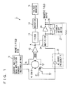
- Fig. 1 is a block diagram showing an entire structure of a SQUID modulation drive circuit.
- Figs. 2A to 2C illustrate a magnetic field - voltage characteristic in the SQUID.
- Figs. 3A and 3B illustrate a magnetic field - voltage characteristic.
- Fig. 4 illustrates a current - voltage characteristic in the SQUID.
- Fig. 5 illustrates a current - voltage characteristic in the SQUID to which AC bias is applied.
- Figs. 6A to 6C illustrate a current - voltage characteristic when AC bias is applied.
- Fig. 7 illustrates a characteristic of change in voltage with time.
- Fig. 8 illustrates change in voltage relative to time with feedback ON.
- Fig. 9 shows the state of Fig. 8 on a voltage monitor.
- Figs. 10 A and 10B illustrate a magnetic field - voltage characteristic after adjustment.
- Fig. 11 shows a display status on the voltage monitor in manual mode.
- Fig. 12 shows magnetic a field - voltage characteristic on the voltage monitor in the manual mode.
- Fig. 13 illustrates a magnetic field - voltage characteristic after adjustment.
- Fig. 14 is a block diagram showing an entire structure of a SQUID modulation drive circuit in a second embodiment.
- Fig. 15 is a block diagram showing a SQUID modulation drive circuit using a conventional FLL.
- a SQUID magnetic flux detection device 1 includes a SQUID 10, a current and magnetic field bias application circuit 11 which applies a predetermined bias current to SQUID 10, a voltage amplifier 12 which amplifies output voltage through both ends of SQUID 10, a filter 13 which passes among components of the voltage amplified by voltage amplifier 12 only a frequency component 2f twice a predetermined frequency f, the frequency component 2f being a modulation signal component described later, a rectifier 14 which rectifies only the frequency component 2f passed through filter 13, and a voltage monitor 15 for monitoring the rectified voltage.
- the voltage amplified by voltage amplifier 12 is fed to a multiplier 24 which supplies a feedback signal for compensating for change of magnetic flux input to SQUID 10 and then to an integrator 25 which determines the integral of the output voltage from multiplier 24, and integrator 25 supplies an output as a measured magnetic field output.
- the output signal from integrator 25 is supplied as a feedback to a coil 21 adjacent to SQUID 10.
- An AC field at frequency f applied from an AC source 23, a field bias with a rectangular wave from current and field bias application circuit 11, and a feedback field from integrator 25 are superimposed on coil 21.
- a capacitor 26 and a feedback ON/OFF switch 27 are provided in parallel with integrator 25.
- a magnetic field bias signal represented by the dotted line shown in Fig. 1 is to be adjusted.
- the adjustment is manually made with observation of voltage monitor 15.
- Fig. 2A is a graph illustrating a relation between magnetic field and output voltage from SQUID 10, the signal waveform taken at the portion indicated by A in Fig. 1.
- Fig. 2B illustrates change of the signal waveform with respect to time, the waveform corresponding to a half period of the signal waveform in Fig 2A.
- the period of the magnetic field is ⁇ 0 in Fig. 2A.
- the amplitude of the voltage resulting from this magnetic field is represented by Vpp. This value changes with application of a bias current Ib from current and field bias application circuit 11, attaining the maximum at a certain optimum value.
- FIG. 2A an arbitrary section corresponding to a half period shown as a bold line is picked out from the waveform.
- the arbitrary section of the waveform corresponding to the half period which changes with time as shown in Fig. 2B.
- the waveform section varies at a modulation frequency f, 40 kHz, applied by AC source 23.
- the voltage changes in half the period ⁇ 0 , from the point indicated by 1 ⁇ to the point 2 ⁇ along the arrow indicated by a , and to the point 3 ⁇ along the arrow indicated by b .
- the change from 1 ⁇ to 3 ⁇ corresponds to the portion represented by the same indications 1 ⁇ to 3 ⁇ on the modulation frequency in Fig. 2B.
- Fig. 2B shows change of the magnetic field in half the period ⁇ 0 with respect to time.
- Fig. 2C shows change of voltage V with time, relative to modulation field in half the period shown in Fig. 2B.
- the indications 1 ⁇ to 3 ⁇ in Fig. 2C also correspond to those in Figs. 2A and 2B.
- Fig. 3A corresponds to Figs. 2A and 2B, showing a magnetic field - voltage characteristic in the half period, the voltage picked out such that the voltage changes between the maximum and minimum values.
- the half period is selected as shown in Fig. 3A in which the voltage changes between the maximum and minimum values, the change of voltage with respect to time coincides with 40 kHz.
- Fig. 3B corresponds to Figs. 2A and 2B, showing a magnetic field - voltage characteristic in the half period, the voltage picked out having the minimum amplitude.
- the signal frequency is 80 kHz, which is twice as high as the modulation frequency.
- the state shown in Fig. 2A is accordingly the intermediate between respective states shown in Figs. 3A and 3B. Therefore, the voltage signal varying with time relative to the modulation field has both of the modulation frequency 40 kHz and twice that frequency, 80 kHz, in the state of Fig. 2A.
- the output voltage of SQUID 10 has a frequency component equal to that of the modulation field and/or a frequency component twice that of the modulation field, and the maximum value of the output Vpp of SQUID 10 is obtained when the sum of the modulation field frequency component and the component twice the modulation field frequency component of the output voltage attains the maximum, i.e. when an optimum bias current value Ib is obtained.
- optimization of magnetic field bias ⁇ b is required when AC bias Ib is applied. Optimization of magnetic field bias ⁇ b enables reduction of low frequency noise if DC bias is applied.
- Fig. 4 shows a current - voltage characteristic of SQUID 10 to which DC bias is applied.
- the optimum bias current value is represented by Ib, which is obtained when the magnetic field applied to SQUID 10 is n times as high as ⁇ 0 .
- Fig. 5 shows a current - voltage characteristic when AC bias is applied.
- current bias +Ib and -Ib are set on the + and - sides.
- Fig. 6A shows a current - voltage characteristic exhibited when the rectangular wave of 1 kHz shown in Fig. 6B is applied as AC bias.
- the bias current values +Ib and -Ib produce respective phases inverted relative to each other, with respect to the same modulation field.
- the output voltage waveforms have respective phases inverted relative to each other with respect to the same modulation field ⁇ .
- Fig. 7 shows the states in Figs. 6A to 6C by using a curve showing voltage change with time that is employed for optimization of bias current Ib as shown in Fig. 2C. Referring to Fig. 7, the time periods in which +Ib and -Ib are applied respectively are illustrated.
- bias current Ib is adjusted as described above, a feedback loop is made ON to effect a flux locked state (feedback ON/OFF switch 27 is turned on).
- Fig. 8 shows change of the output voltage with respect to time.
- this status is displayed as shown in Fig. 9 on voltage monitor 15 in Fig. 1. Specifically, orderly curved waveforms in phase with each other appear to be arranged shifted from each other. A frequency component of 80 kHz which is twice the modulation frequency is to be output in this way.
- Modulation field offsets having the same absolute value and different polarities are applied depending on the polarities of current bias.
- respective phases of output voltages when the current biases are + and - respectively change by the same phase amount in a direction to allow phases to match with each other. (Although the phases could seemingly separate from each other, they match every 360°.) Consequently, the voltages are in phase with each other at a certain point as shown in Figs. 10A and 10B.
- Fig. 10A illustrates a modulation field - voltage characteristic
- Fig. 10B illustrates change of the modulation field with respect to time.
- the output signal has only the component of 80 kHz. Optimization of the magnetic field bias is thus achieved by maximizing the frequency component which is twice the modulation frequency. Accordingly, the sum of modulation field frequency component and component twice the modulation field frequency is maximized to optimize current bias Ib, and then feedback is performed.
- the magnetic field bias is optimized by making adjustment such that the sum of modulation field frequency component and component twice the modulation field frequency is the maximum. Finally, re-lock (feedback) is done.
- the magnetic field bias is adjusted in manual mode by matching phases for +Ib and -Ib respectively and then performing feedback.
- current bias Ib is adjusted on voltage monitor 15 such as an oscilloscope, then the phases as shown in Fig. 11 are adjusted by magnetic field bias as shown in Fig. 12, and the following feedback provides the operating state as shown in Fig. 13.
- Fig. 14 is a circuit diagram in the second embodiment that corresponds to Fig. 1.
- magnetic field bias is automatically adjusted by using a personal computer 17 in the second embodiment. Specifically, a rectified analog signal is transformed to a digital signal by an A/D converter 16, and the digital signal is input to personal computer 17 to automatically control the magnetic field bias via a current and field bias application circuit 22.
- Other components and operations are identical to those of the first embodiment, and the identical components are represented accordingly by the same reference characters and description thereof is not repeated here.
Abstract
Description
- The present invention relates to a method and a device for adjusting magnetic field bias in a modulation drive circuit for a superconducting quantum interference device (hereinafter referred to as SQUID). In particular, the invention relates to a method and a device for easily adjusting magnetic field bias in a SQUID modulation drive circuit.
- Fig. 15 is a circuit diagram showing a conventional control circuit for a SQUID with a flux locked loop (hereinafter referred to as FLL). Referring to Fig. 15, the conventional SQUID FLL circuit includes a SQUID 81 having two Josephson junctions formed at predetermined positions and a constant
current source 88 supplying constant current to SQUID 81. Magnetic flux to be measured is input from a pickup coil (not shown) toSQUID 81. Voltage output through both ends of SQUID 81 is converted by a transformer, amplified by apreamplifier 83 and then output from an output portion through amultiplier 84 and anintegrator 85. A modulation signal at 40 kHz is added by a modulatingunit 87 to the output frommultiplier 84 for feedback to afield application coil 82 adjacent toSQUID 81. Accordingly, external magnetic flux detected at SQUID 81 is cancelled. - The output from SQUID 81 is also fed to an
oscilloscope 90 provided separately from the output portion for observing the waveform thereof. Specifically, a feedback signal is partially input to the X axis ofoscilloscope 90 and an output frompreamplifier 83 is input to the Y axis ofoscilloscope 90. - As a method of reducing low frequency noise, an AC biasing method is known. According to the AC biasing method, positive and negative currents having the same absolute value (the absolute value is equal to that of the constant current) are applied to a SQUID. In order to achieve a stable feedback, both outputs from the SQUID to which the positive and negative current biases are being applied should be in phase with each other. In order to achieve this, magnetic field bias is adjusted to match the phases with each other.
- The magnetic field bias has conventionally been adjusted by manually adjusting the phase of voltage waveform on
oscilloscope 90 while observing change of voltage relative to the magnetic field, with respect to time. This method has a problem that adjustment of the magnetic field bias is extremely complicated and time-consuming. - One object of the present invention is accordingly to provide a method of easily adjusting magnetic field bias in a modulation drive circuit for a SQUID.
- Another object of the present invention is to provide a device for easily adjusting magnetic field bias in a modulation drive circuit for a SQUID.
- The objects above are accomplished by a method of adjusting magnetic field bias in a SQUID modulation drive circuit that includes following steps. Specifically, according to one aspect of the present invention, a method of adjusting magnetic field bias in a SQUID modulation drive circuit includes the steps of applying a modulation signal at a predetermined first frequency to a flux locked loop maintaining magnetic flux supplied to the SQUID at a constant value, picking out an output voltage from the SQUID to which a predetermined bias current is being applied, and picking out the output voltage such that a frequency component of the voltage which is twice as high as the first frequency is a maximum frequency.
- The output voltage is picked out from the SQUID to which a predetermined modulation frequency is being applied and then the frequency component of the output voltage twice the frequency of the applied predetermined modulation frequency is maximized, so that the magnetic field bias can be optimized easily.
- Preferably, the step of applying to the flux locked loop the modulation signal at the predetermined first frequency includes the step of applying the modulation signal at the predetermined first frequency to a coil adjacent to the SQUID, and the magnetic field bias is thus adjusted by applying magnetic field bias to the coil adjacent to the SQUID.
- A method of adjusting magnetic field bias can thus be provided with a simple structure since the magnetic field bias is adjusted by applying magnetic field bias to a coil adjacent to the SQUID, to which a modulation signal at a predetermined frequency is applied.
- The magnetic field bias may be adjusted manually. A low cost method of adjusting magnetic field bias can accordingly be provided.
- The magnetic field bias may be adjusted automatically. A laborsaving method of adjusting magnetic field bias can accordingly be provided.
- The bias current may be alternating current or direct current.
- According to another aspect of the invention, a device for adjusting magnetic field bias in a SQUID modulation drive circuit includes a unit for applying a modulation signal at a predetermined first frequency to a flux locked loop maintaining magnetic flux supplied to the SQUID at a constant value, a unit for picking out an output voltage from the SQUID to which a predetermined bias current is being applied, and a filter for picking out the output voltage such that a frequency component of the voltage which is twice as high as the first frequency is a maximum frequency.
- The foregoing and other objects, features, aspects and advantages of the present invention will become more apparent from the following detailed description of the present invention when taken in conjunction with the accompanying drawings.
- Fig. 1 is a block diagram showing an entire structure of a SQUID modulation drive circuit.
- Figs. 2A to 2C illustrate a magnetic field - voltage characteristic in the SQUID.
- Figs. 3A and 3B illustrate a magnetic field - voltage characteristic.
- Fig. 4 illustrates a current - voltage characteristic in the SQUID.
- Fig. 5 illustrates a current - voltage characteristic in the SQUID to which AC bias is applied.
- Figs. 6A to 6C illustrate a current - voltage characteristic when AC bias is applied.
- Fig. 7 illustrates a characteristic of change in voltage with time.
- Fig. 8 illustrates change in voltage relative to time with feedback ON.
- Fig. 9 shows the state of Fig. 8 on a voltage monitor.
- Figs. 10 A and 10B illustrate a magnetic field - voltage characteristic after adjustment.
- Fig. 11 shows a display status on the voltage monitor in manual mode.
- Fig. 12 shows magnetic a field - voltage characteristic on the voltage monitor in the manual mode.
- Fig. 13 illustrates a magnetic field - voltage characteristic after adjustment.
- Fig. 14 is a block diagram showing an entire structure of a SQUID modulation drive circuit in a second embodiment.
- Fig. 15 is a block diagram showing a SQUID modulation drive circuit using a conventional FLL.
- Embodiments of the present invention will be described below in conjunction with the drawings.
- Referring to Fig. 1, a SQUID magnetic
flux detection device 1 includes aSQUID 10, a current and magnetic fieldbias application circuit 11 which applies a predetermined bias current toSQUID 10, avoltage amplifier 12 which amplifies output voltage through both ends ofSQUID 10, afilter 13 which passes among components of the voltage amplified byvoltage amplifier 12 only a frequency component 2f twice a predetermined frequency f, the frequency component 2f being a modulation signal component described later, arectifier 14 which rectifies only the frequency component 2f passed throughfilter 13, and avoltage monitor 15 for monitoring the rectified voltage. - The voltage amplified by
voltage amplifier 12 is fed to amultiplier 24 which supplies a feedback signal for compensating for change of magnetic flux input toSQUID 10 and then to anintegrator 25 which determines the integral of the output voltage frommultiplier 24, andintegrator 25 supplies an output as a measured magnetic field output. The output signal fromintegrator 25 is supplied as a feedback to acoil 21 adjacent toSQUID 10. An AC field at frequency f applied from anAC source 23, a field bias with a rectangular wave from current and fieldbias application circuit 11, and a feedback field fromintegrator 25 are superimposed oncoil 21. Acapacitor 26 and a feedback ON/OFF switch 27 are provided in parallel withintegrator 25. - Adjustment in the circuit shown in Fig. 1 is described now. A magnetic field bias signal represented by the dotted line shown in Fig. 1 is to be adjusted. In the first embodiment, the adjustment is manually made with observation of
voltage monitor 15. - Specific description is now given. Fig. 2A is a graph illustrating a relation between magnetic field and output voltage from
SQUID 10, the signal waveform taken at the portion indicated by A in Fig. 1. Fig. 2B illustrates change of the signal waveform with respect to time, the waveform corresponding to a half period of the signal waveform in Fig 2A. The period of the magnetic field is Φ0 in Fig. 2A. The amplitude of the voltage resulting from this magnetic field is represented by Vpp. This value changes with application of a bias current Ib from current and fieldbias application circuit 11, attaining the maximum at a certain optimum value. - Referring to Fig. 2A, an arbitrary section corresponding to a half period shown as a bold line is picked out from the waveform. The arbitrary section of the waveform corresponding to the half period which changes with time as shown in Fig. 2B. The waveform section varies at a modulation frequency f, 40 kHz, applied by
AC source 23. In Fig. 2A, the voltage changes in half the period Φ0, from the point indicated by 1 ○ to thepoint 2 ○ along the arrow indicated by a, and to thepoint 3 ○ along the arrow indicated by b. The change from 1 ○ to 3 ○ corresponds to the portion represented by thesame indications 1 ○ to 3 ○ on the modulation frequency in Fig. 2B. In other words, Fig. 2B shows change of the magnetic field in half the period Φ0 with respect to time. - Fig. 2C shows change of voltage V with time, relative to modulation field in half the period shown in Fig. 2B. The
indications 1 ○ to 3 ○ in Fig. 2C also correspond to those in Figs. 2A and 2B. - Fig. 3A corresponds to Figs. 2A and 2B, showing a magnetic field - voltage characteristic in the half period, the voltage picked out such that the voltage changes between the maximum and minimum values. When the half period is selected as shown in Fig. 3A in which the voltage changes between the maximum and minimum values, the change of voltage with respect to time coincides with 40 kHz.
- Fig. 3B corresponds to Figs. 2A and 2B, showing a magnetic field - voltage characteristic in the half period, the voltage picked out having the minimum amplitude. When the voltage in this state changing with time is picked out, as shown in Fig. 3B, the signal frequency is 80 kHz, which is twice as high as the modulation frequency.
- The state shown in Fig. 2A is accordingly the intermediate between respective states shown in Figs. 3A and 3B. Therefore, the voltage signal varying with time relative to the modulation field has both of the modulation frequency 40 kHz and twice that frequency, 80 kHz, in the state of Fig. 2A.
- Accordingly, the output voltage of
SQUID 10 has a frequency component equal to that of the modulation field and/or a frequency component twice that of the modulation field, and the maximum value of the output Vpp ofSQUID 10 is obtained when the sum of the modulation field frequency component and the component twice the modulation field frequency component of the output voltage attains the maximum, i.e. when an optimum bias current value Ib is obtained. - Optimization of magnetic field bias Φb is required when AC bias Ib is applied. Optimization of magnetic field bias Φb enables reduction of low frequency noise if DC bias is applied.
- Fig. 4 shows a current - voltage characteristic of
SQUID 10 to which DC bias is applied. The optimum bias current value is represented by Ib, which is obtained when the magnetic field applied toSQUID 10 is n times as high as Φ0. - Fig. 5 shows a current - voltage characteristic when AC bias is applied. In this case, current bias +Ib and -Ib are set on the + and - sides.
- Fig. 6A shows a current - voltage characteristic exhibited when the rectangular wave of 1 kHz shown in Fig. 6B is applied as AC bias. The bias current values +Ib and -Ib produce respective phases inverted relative to each other, with respect to the same modulation field. As a result, the output voltage waveforms have respective phases inverted relative to each other with respect to the same modulation field Φ.
- Fig. 7 shows the states in Figs. 6A to 6C by using a curve showing voltage change with time that is employed for optimization of bias current Ib as shown in Fig. 2C. Referring to Fig. 7, the time periods in which +Ib and -Ib are applied respectively are illustrated.
- After bias current Ib is adjusted as described above, a feedback loop is made ON to effect a flux locked state (feedback ON/
OFF switch 27 is turned on). - In the time periods in which bias currents +Ib and -Ib are applied respectively, the phases do not match and there is generated an unstable state. The circuit operates in this case to output a waveform which achieves a normal feedback status as shown in Fig. 8. Fig. 8 shows change of the output voltage with respect to time.
- Actually, this status is displayed as shown in Fig. 9 on voltage monitor 15 in Fig. 1. Specifically, orderly curved waveforms in phase with each other appear to be arranged shifted from each other. A frequency component of 80 kHz which is twice the modulation frequency is to be output in this way.
- Modulation field offsets having the same absolute value and different polarities are applied depending on the polarities of current bias. By changing the absolute value, respective phases of output voltages when the current biases are + and - respectively change by the same phase amount in a direction to allow phases to match with each other. (Although the phases could seemingly separate from each other, they match every 360°.) Consequently, the voltages are in phase with each other at a certain point as shown in Figs. 10A and 10B. Fig. 10A illustrates a modulation field - voltage characteristic and Fig. 10B illustrates change of the modulation field with respect to time.
- As shown in Figs. 10A and 10B, the output signal has only the component of 80 kHz. Optimization of the magnetic field bias is thus achieved by maximizing the frequency component which is twice the modulation frequency. Accordingly, the sum of modulation field frequency component and component twice the modulation field frequency is maximized to optimize current bias Ib, and then feedback is performed. The magnetic field bias is optimized by making adjustment such that the sum of modulation field frequency component and component twice the modulation field frequency is the maximum. Finally, re-lock (feedback) is done.
- It is noted that the magnetic field bias is adjusted in manual mode by matching phases for +Ib and -Ib respectively and then performing feedback. For example, current bias Ib is adjusted on voltage monitor 15 such as an oscilloscope, then the phases as shown in Fig. 11 are adjusted by magnetic field bias as shown in Fig. 12, and the following feedback provides the operating state as shown in Fig. 13.
- The second embodiment is now described. Fig. 14 is a circuit diagram in the second embodiment that corresponds to Fig. 1. Referring to Fig. 14, magnetic field bias is automatically adjusted by using a
personal computer 17 in the second embodiment. Specifically, a rectified analog signal is transformed to a digital signal by an A/D converter 16, and the digital signal is input topersonal computer 17 to automatically control the magnetic field bias via a current and fieldbias application circuit 22. Other components and operations are identical to those of the first embodiment, and the identical components are represented accordingly by the same reference characters and description thereof is not repeated here. - Although the present invention has been described and illustrated in detail, it is clearly understood that the same is by way of illustration and example only and is not to be taken by way of limitation, the spirit and scope of the present invention being limited only by the terms of the appended claims.
Claims (12)
- A method of adjusting magnetic field bias in a modulation drive circuit for a SQUID (10), comprising the steps of:applying a modulation signal at a predetermined first frequency to a flux locked loop maintaining magnetic flux supplied to said SQUID (10) at a constant value;picking out output voltage from said SQUID (10) to which a predetermined bias current is being applied; andpicking out said output voltage such that a frequency component of the voltage which is twice as high as said first frequency is a maximum frequency component.
- The magnetic field bias adjusting method according to claim 1, whereinsaid step of applying the modulation signal at the predetermined first frequency to said flux locked loop includes the step of applying said modulation signal at the predetermined first frequency to a coil (21) adjacent to said SQUID (10), andsaid magnetic field bias is adjusted by applying magnetic field bias to said coil (21) adjacent to said SQUID (10).
- The magnetic field bias adjusting method according to claim 2, wherein
said magnetic field bias is manually adjusted. - The magnetic field bias adjusting method according to claim 2, wherein
said magnetic field bias is automatically adjusted. - The magnetic field bias adjusting method according to claim 2, wherein
said bias current is alternating current. - The magnetic field bias adjusting method according to claim 2, wherein
said bias current is direct current. - A device for adjusting magnetic field bias in a modulation drive circuit for a SQUID (10), comprising:means (23) for applying a modulation signal at a predetermined first frequency to a flux locked loop maintaining magnetic flux supplied to said SQUID at a constant value;means (12) for picking out output voltage from said SQUID (10) to which a predetermined bias current is being applied; anda filter (13) for picking out said output voltage such that a frequency component of the voltage which is twice as high as said first frequency is a maximum frequency component.
- The magnetic field bias adjusting device according to claim 7, further comprising a coil (21) adjacent to said SQUID (10), whereinsaid means (23) for applying the modulation signal at the predetermined first frequency applies said modulation signal at the predetermined first frequency to said coil (21), andsaid magnetic field bias is adjusted by applying magnetic field bias to said coil (21).
- The magnetic field bias adjusting device according to claim 8, wherein
said magnetic field bias is manually adjusted. - The magnetic field bias adjusting device according to claim 8, wherein
said magnetic field bias is automatically adjusted. - The magnetic field bias adjusting device according to claim 8, wherein
said bias current is alternating current. - The magnetic field bias adjusting device according to claim 8, wherein
said bias current is direct current.
Applications Claiming Priority (2)
| Application Number | Priority Date | Filing Date | Title |
|---|---|---|---|
| JP11132086A JP2000321343A (en) | 1999-05-13 | 1999-05-13 | Method and device for adjusting magnetic field bias in modulation drive circuit for squid |
| JP13208699 | 1999-05-13 |
Publications (3)
| Publication Number | Publication Date |
|---|---|
| EP1054262A2 true EP1054262A2 (en) | 2000-11-22 |
| EP1054262A3 EP1054262A3 (en) | 2001-04-11 |
| EP1054262B1 EP1054262B1 (en) | 2006-08-23 |
Family
ID=15073181
Family Applications (1)
| Application Number | Title | Priority Date | Filing Date |
|---|---|---|---|
| EP00401307A Expired - Lifetime EP1054262B1 (en) | 1999-05-13 | 2000-05-12 | Magnetic field bias adjusting method and device for a SQUID modulation drive circuit |
Country Status (7)
| Country | Link |
|---|---|
| US (1) | US6388440B1 (en) |
| EP (1) | EP1054262B1 (en) |
| JP (1) | JP2000321343A (en) |
| KR (1) | KR20000077237A (en) |
| CA (1) | CA2304839A1 (en) |
| DE (1) | DE60030199T2 (en) |
| NO (1) | NO322383B1 (en) |
Families Citing this family (8)
| Publication number | Priority date | Publication date | Assignee | Title |
|---|---|---|---|---|
| JP2002148322A (en) * | 2000-11-09 | 2002-05-22 | Seiko Instruments Inc | Signal detector using superconducting quantum interference element and its measuring method |
| US20040163578A1 (en) * | 2003-02-21 | 2004-08-26 | Mcdonald Roger C. | Seed eductor assembly |
| DE10312172B4 (en) * | 2003-03-14 | 2007-06-28 | Institut für Physikalische Hochtechnologie e.V. | Method for operating a SQUID and device for carrying out the method |
| JP5758450B2 (en) * | 2013-07-18 | 2015-08-05 | 株式会社フジクラ | Magnetic sensor driving circuit, magnetic sensor, current sensor, and magnetic sensor driving method |
| CN104422903B (en) * | 2013-08-23 | 2017-09-26 | 中国科学院上海微系统与信息技术研究所 | Debugging system and method for the sensor using SPUID |
| CN104198961B (en) * | 2014-07-18 | 2017-06-13 | 中国科学院上海微系统与信息技术研究所 | Using the superconducting quantum interference device Magnetic Sensor of single operational amplifier |
| CN106019181B (en) * | 2016-05-13 | 2018-09-25 | 中国科学院上海微系统与信息技术研究所 | The superconducting quantum interference device Magnetic Sensor and detection method of high speed wide range |
| JP2018124156A (en) * | 2017-01-31 | 2018-08-09 | 富士通株式会社 | FLL circuit and SQUID sensor |
Citations (5)
| Publication number | Priority date | Publication date | Assignee | Title |
|---|---|---|---|---|
| JPH03131781A (en) * | 1989-10-18 | 1991-06-05 | Hitachi Ltd | Squid fluxmeter measurement system |
| EP0499968A2 (en) * | 1991-02-22 | 1992-08-26 | Seiko Instruments Inc. | Highly sensitive magnetic field detecting device |
| JPH04340488A (en) * | 1991-05-17 | 1992-11-26 | Seiko Instr Inc | Highly-sensitive apparatus for detecting magnetic field |
| US5291135A (en) * | 1990-09-28 | 1994-03-01 | Hitachi Ltd. | Weak magnetic field measuring system using dc-SQUID magnetometer with bias current adjustment and/or detecting function of abnormal operation |
| EP0837337A2 (en) * | 1996-10-17 | 1998-04-22 | Sumitomo Electric Industries, Limited | Circuit device for driving magnetometric sensor |
Family Cites Families (4)
| Publication number | Priority date | Publication date | Assignee | Title |
|---|---|---|---|---|
| JPH01269074A (en) * | 1988-04-20 | 1989-10-26 | Hitachi Ltd | Squid fluxmeter |
| JPH0660934B2 (en) * | 1990-09-28 | 1994-08-10 | 通商産業省工業技術院長 | DC SQUID magnetometer |
| JPH05312929A (en) * | 1992-05-15 | 1993-11-26 | Fujitsu Ltd | Magnetic-flux measuring apparatus using digital superconducting quantum interferrometer |
| KR100198555B1 (en) * | 1996-04-25 | 1999-06-15 | 구자홍 | Magnetometer |
-
1999
- 1999-05-13 JP JP11132086A patent/JP2000321343A/en active Pending
-
2000
- 2000-04-11 CA CA002304839A patent/CA2304839A1/en not_active Abandoned
- 2000-04-13 US US09/548,737 patent/US6388440B1/en not_active Expired - Fee Related
- 2000-05-12 EP EP00401307A patent/EP1054262B1/en not_active Expired - Lifetime
- 2000-05-12 DE DE60030199T patent/DE60030199T2/en not_active Expired - Fee Related
- 2000-05-12 KR KR1020000025273A patent/KR20000077237A/en not_active Application Discontinuation
- 2000-05-12 NO NO20002491A patent/NO322383B1/en not_active IP Right Cessation
Patent Citations (5)
| Publication number | Priority date | Publication date | Assignee | Title |
|---|---|---|---|---|
| JPH03131781A (en) * | 1989-10-18 | 1991-06-05 | Hitachi Ltd | Squid fluxmeter measurement system |
| US5291135A (en) * | 1990-09-28 | 1994-03-01 | Hitachi Ltd. | Weak magnetic field measuring system using dc-SQUID magnetometer with bias current adjustment and/or detecting function of abnormal operation |
| EP0499968A2 (en) * | 1991-02-22 | 1992-08-26 | Seiko Instruments Inc. | Highly sensitive magnetic field detecting device |
| JPH04340488A (en) * | 1991-05-17 | 1992-11-26 | Seiko Instr Inc | Highly-sensitive apparatus for detecting magnetic field |
| EP0837337A2 (en) * | 1996-10-17 | 1998-04-22 | Sumitomo Electric Industries, Limited | Circuit device for driving magnetometric sensor |
Non-Patent Citations (2)
| Title |
|---|
| PATENT ABSTRACTS OF JAPAN vol. 015, no. 347 (P-1246), 3 September 1991 (1991-09-03) -& JP 03 131781 A (HITACHI LTD), 5 June 1991 (1991-06-05) * |
| PATENT ABSTRACTS OF JAPAN vol. 017, no. 189 (P-1521), 13 April 1993 (1993-04-13) -& JP 04 340488 A (SEIKO INSTR INC), 26 November 1992 (1992-11-26) * |
Also Published As
| Publication number | Publication date |
|---|---|
| DE60030199T2 (en) | 2007-07-26 |
| NO322383B1 (en) | 2006-09-25 |
| NO20002491L (en) | 2000-11-14 |
| KR20000077237A (en) | 2000-12-26 |
| US6388440B1 (en) | 2002-05-14 |
| EP1054262B1 (en) | 2006-08-23 |
| CA2304839A1 (en) | 2000-11-13 |
| DE60030199D1 (en) | 2006-10-05 |
| NO20002491D0 (en) | 2000-05-12 |
| JP2000321343A (en) | 2000-11-24 |
| EP1054262A3 (en) | 2001-04-11 |
Similar Documents
| Publication | Publication Date | Title |
|---|---|---|
| EP1903228B1 (en) | Magnetic bearing device and magnetic bearing method | |
| US5469057A (en) | Method and apparatus for extending the dynamic range of DC-squid measurements using a flux tracking loop | |
| US6388440B1 (en) | Magnetic field bias adjusting device for SQUID modulation drive circuit achieving easy adjustment | |
| EP0427412A2 (en) | Current measuring method and apparatus therefor | |
| WO2005112239A2 (en) | Power converter apparatus and methods using a phase reference derived from a dc bus voltage | |
| KR20020027491A (en) | Ac current detection device | |
| EP0499968B1 (en) | Highly sensitive magnetic field detecting device | |
| US6498483B1 (en) | Device and method for easily adjusting working point of SQUID | |
| JP4269445B2 (en) | SQUID magnetic field detector | |
| JP2018207785A (en) | Power converter | |
| EP0501241B1 (en) | Highly sensitive magnetic field detecting device | |
| JPH07280903A (en) | Superconducting magnetometer | |
| JP3198746B2 (en) | SQUID magnetometer | |
| US5900730A (en) | Magnetometer using two squids | |
| JP3387445B2 (en) | SQUID operating point adjustment device and method | |
| JP2000292511A (en) | Apparatus and method for adjusting operating point of squid | |
| JPH0868834A (en) | Superconducting magnetometer | |
| JPH03131781A (en) | Squid fluxmeter measurement system | |
| JPH09257895A (en) | Magnetometer | |
| CN116780884A (en) | Power factor correction circuit | |
| JPH04208886A (en) | Multi-input magnetic field detector | |
| JPH0572235A (en) | Current detector and dc power supply device using the same | |
| Furukawa et al. | Proposal for a Beat Oscillating Superconducting Quantum Interference Device | |
| JPH09230014A (en) | Low noise squid magnetic fluxmeter | |
| JPH01199177A (en) | Superconducting magnetometer |
Legal Events
| Date | Code | Title | Description |
|---|---|---|---|
| PUAI | Public reference made under article 153(3) epc to a published international application that has entered the european phase |
Free format text: ORIGINAL CODE: 0009012 |
|
| AK | Designated contracting states |
Kind code of ref document: A2 Designated state(s): DE FR GB IT |
|
| AX | Request for extension of the european patent |
Free format text: AL;LT;LV;MK;RO;SI |
|
| PUAL | Search report despatched |
Free format text: ORIGINAL CODE: 0009013 |
|
| AK | Designated contracting states |
Kind code of ref document: A3 Designated state(s): AT BE CH CY DE DK ES FI FR GB GR IE IT LI LU MC NL PT SE |
|
| AX | Request for extension of the european patent |
Free format text: AL;LT;LV;MK;RO;SI |
|
| 17P | Request for examination filed |
Effective date: 20010618 |
|
| AKX | Designation fees paid |
Free format text: DE FR GB IT |
|
| 17Q | First examination report despatched |
Effective date: 20020228 |
|
| GRAP | Despatch of communication of intention to grant a patent |
Free format text: ORIGINAL CODE: EPIDOSNIGR1 |
|
| RTI1 | Title (correction) |
Free format text: MAGNETIC FIELD BIAS ADJUSTING METHOD AND DEVICE FOR A SQUID MODULATION DRIVE CIRCUIT |
|
| GRAS | Grant fee paid |
Free format text: ORIGINAL CODE: EPIDOSNIGR3 |
|
| GRAA | (expected) grant |
Free format text: ORIGINAL CODE: 0009210 |
|
| AK | Designated contracting states |
Kind code of ref document: B1 Designated state(s): DE FR GB IT |
|
| PG25 | Lapsed in a contracting state [announced via postgrant information from national office to epo] |
Ref country code: IT Free format text: LAPSE BECAUSE OF FAILURE TO SUBMIT A TRANSLATION OF THE DESCRIPTION OR TO PAY THE FEE WITHIN THE PRESCRIBED TIME-LIMIT;WARNING: LAPSES OF ITALIAN PATENTS WITH EFFECTIVE DATE BEFORE 2007 MAY HAVE OCCURRED AT ANY TIME BEFORE 2007. THE CORRECT EFFECTIVE DATE MAY BE DIFFERENT FROM THE ONE RECORDED. Effective date: 20060823 |
|
| REG | Reference to a national code |
Ref country code: GB Ref legal event code: FG4D |
|
| REF | Corresponds to: |
Ref document number: 60030199 Country of ref document: DE Date of ref document: 20061005 Kind code of ref document: P |
|
| EN | Fr: translation not filed | ||
| PLBE | No opposition filed within time limit |
Free format text: ORIGINAL CODE: 0009261 |
|
| STAA | Information on the status of an ep patent application or granted ep patent |
Free format text: STATUS: NO OPPOSITION FILED WITHIN TIME LIMIT |
|
| 26N | No opposition filed |
Effective date: 20070524 |
|
| GBPC | Gb: european patent ceased through non-payment of renewal fee |
Effective date: 20070512 |
|
| PG25 | Lapsed in a contracting state [announced via postgrant information from national office to epo] |
Ref country code: FR Free format text: LAPSE BECAUSE OF FAILURE TO SUBMIT A TRANSLATION OF THE DESCRIPTION OR TO PAY THE FEE WITHIN THE PRESCRIBED TIME-LIMIT Effective date: 20070511 |
|
| PG25 | Lapsed in a contracting state [announced via postgrant information from national office to epo] |
Ref country code: GB Free format text: LAPSE BECAUSE OF NON-PAYMENT OF DUE FEES Effective date: 20070512 |
|
| PG25 | Lapsed in a contracting state [announced via postgrant information from national office to epo] |
Ref country code: FR Free format text: LAPSE BECAUSE OF FAILURE TO SUBMIT A TRANSLATION OF THE DESCRIPTION OR TO PAY THE FEE WITHIN THE PRESCRIBED TIME-LIMIT Effective date: 20060823 |
|
| PGFP | Annual fee paid to national office [announced via postgrant information from national office to epo] |
Ref country code: DE Payment date: 20090511 Year of fee payment: 10 |
|
| PG25 | Lapsed in a contracting state [announced via postgrant information from national office to epo] |
Ref country code: DE Free format text: LAPSE BECAUSE OF NON-PAYMENT OF DUE FEES Effective date: 20101201 |