EP1052782A1 - Mobiltelefon mit einer Demodulationsschaltung mit einem verbesserten Überlagerungsoszillator - Google Patents
Mobiltelefon mit einer Demodulationsschaltung mit einem verbesserten Überlagerungsoszillator Download PDFInfo
- Publication number
- EP1052782A1 EP1052782A1 EP00401220A EP00401220A EP1052782A1 EP 1052782 A1 EP1052782 A1 EP 1052782A1 EP 00401220 A EP00401220 A EP 00401220A EP 00401220 A EP00401220 A EP 00401220A EP 1052782 A1 EP1052782 A1 EP 1052782A1
- Authority
- EP
- European Patent Office
- Prior art keywords
- frequency
- signal
- oscillator
- excess
- khz
- Prior art date
- Legal status (The legal status is an assumption and is not a legal conclusion. Google has not performed a legal analysis and makes no representation as to the accuracy of the status listed.)
- Granted
Links
Images
Classifications
-
- H—ELECTRICITY
- H04—ELECTRIC COMMUNICATION TECHNIQUE
- H04B—TRANSMISSION
- H04B1/00—Details of transmission systems, not covered by a single one of groups H04B3/00 - H04B13/00; Details of transmission systems not characterised by the medium used for transmission
- H04B1/06—Receivers
- H04B1/16—Circuits
- H04B1/30—Circuits for homodyne or synchrodyne receivers
-
- H—ELECTRICITY
- H04—ELECTRIC COMMUNICATION TECHNIQUE
- H04L—TRANSMISSION OF DIGITAL INFORMATION, e.g. TELEGRAPHIC COMMUNICATION
- H04L27/00—Modulated-carrier systems
- H04L27/18—Phase-modulated carrier systems, i.e. using phase-shift keying
- H04L27/22—Demodulator circuits; Receiver circuits
- H04L27/233—Demodulator circuits; Receiver circuits using non-coherent demodulation
- H04L27/2332—Demodulator circuits; Receiver circuits using non-coherent demodulation using a non-coherent carrier
Definitions
- the subject of the present invention is a demodulation circuit with improved local oscillator, usable mainly in the field of cellular telephony, in particular of GSM type.
- recognition protocols are instituted at the time of implementation mobile phone service in a network. These protocols impose technical constraints difficult to satisfy for the equipment of mobile phones.
- the object of the present invention is to resolve effectively a problem that arises at the time of commissioning and which, in the state of the art, can only be resolved by choosing perfect local oscillators, and whose cost of development is excessive.
- beacon signal transmitted by the base station of a cell has different types of signals that are needed to the hanging of new mobile phones in the cell, and the maintenance under surveillance of mobile phones already present.
- This beacon signal is generally emitted at a fixed beacon frequency Fi. From one cell to another Fi may vary. In some cases some adjacent cells may share the same beacon frequency.
- the signal sent to the beacon frequency is emitted at a higher power level than the signals useful for communications exchanged between the base station of the cell and a mobile phone even the most distant from this base station in this cell.
- the beacon signal is also permanent. Well who is cut into frames, and in these frames in time windows whose meaning changes from one window to another, the program is constant and at same level of power.
- the beacon signal is formed by a pattern repeated after a certain number of frames, by examples 51 frames within the framework of GSM. Duration a time window being 577 microseconds and in this example a frame comprising eight windows, the duration of a frame is 4.615 milliseconds while the duration of a pattern is of the order of 235 milliseconds. This pattern has groupings of ten or eleven frames.
- a first grouping of frames of this pattern is different from a next grouping. It includes in each of the ten frames which the consists respectively of so-called FCH, SCH, BCCH and CCCH signals.
- the FCH signals mean Frequency Control cHannel whose translation is frequency correction channel. They correspond to a broadcast of a carrier Fi (that of the beacon) modulated by a pure sinusoid at 67.7 KHz from the center of the canal. Such a modulation frequency in fact results in GSM type coding with a twelve-fold modulation constellation points, to transmit I and Q coding values successively (1,0), (0,1), (-1,0) and (0, -1) and to repeat these codings.
- the broadcast of the modulated carrier lasts for a whole time window.
- a mobile phone which has just been put into service can thus first find out which carrier is receiving the most power.
- the mobile phone searches for a carrier at a tag frequency it receives best. This is achieved by scanning in the band and by simple detection, carried out for example directly at the output of a reception circuit, even before demodulation.
- the scrutiny thus involves observing what is happening in wide channels standardized, 200 KHz for GSM. Indeed, while the carrier frequencies dedicated to the transmission of communication are subject to frequency agility, a window time to another, the beacon frequency Fi is kept constant. he It is therefore enough for a mobile phone to listen successively to all bands to know which one is the best received.
- the phone mobile seeks to detect what is the time window during which it receives an FCH signal modulating this carrier Fi by a pure sinusoid at 67.7 KHz. It is in this research that appear more particularly the problems solved by the invention. Indeed, given the width imposed for channels, 200 KHz, demodulators of demodulation circuits normally have a filter, called channel filter, at the output. The width of band of a channel filter, at low frequency, goes from - 100 KHz to + 100 KHz. In fact, demodulation transposes the modulated signal by mixing the signal received with a signal at the carrier frequency Fi produced by a local oscillator. However, this demodulation is not carried out perfectly due to the imprecision of the local oscillator. Yes the local oscillator, instead of producing a signal at a frequency Fi produces a signal at a frequency Fi - ⁇ , the demodulated signal at output will have a frequency equal to 67.7 KHz + ⁇ .
- the local oscillator can be set so that £ is low or zero.
- the difference ⁇ tolerated must be less than 23.5 parts per million (ppm) for the GSM band at 900 MHz and below at 12.1 ppm in the DCS band at 1800 MHz, and is also less than 11.4 ppm in the PCS band at 2100 MHz. This avoids demodulation problems due to the presence of the channel filter.
- correction circuits are provided in a mobile telephone for measure the difference ⁇ and to modify the value of the demodulated signals by match (not to change the demodulation frequency Fi + ⁇ ).
- the frequency of the local oscillator may drift. This drift may be large enough that the presence of the channel disrupts the reception and demodulation of the signal at the frequency of 67.7 KHz. Indeed the band of the channel filter, at the edge of band around 100 KHz, is not steep but has a slope significant. In practice, the damping of received signals starts well before a limit frequency of 100 KHz. Note that with regard to the reception of communication signals, this progressive cut-off (which also offers the advantage of a simpler realization of the channel filter and of a less penalizing phase rotation) is not annoying because the amount of information transmitted by hertz at the edge of the band is low. Most of the information is included in the low frequencies demodulated.
- the offset ⁇ ' (expressed in absolute terms) is small. Her contribution can be easily compensated by the correction circuits of known type already in place in reception circuits, and which have the effect to neutralize the offset ⁇ envisaged in the state of the art.
- the offset ⁇ 'of the local oscillator is obviously performed by excess so that the demodulated FCH signal is rather drawn towards the low frequencies, and becomes a signal below 67.7 KHz rather than high frequencies where, being well above 67.7 KHz, it would risk reaching the channel filter cut-off strip, and where its damping would prevent simply its correct detection.
- the invention therefore relates to a mobile telephone provided with a circuit demodulation comprising a local oscillator and a mixer with a local oscillator input and a demodulation input, the input of demodulation receiving a signal modulating a carrier at a frequency Fi, characterized in that the local oscillator is out of tune with respect to at the frequency Fi.
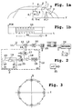
- Figure 1a shows a spectral diagram 1 of a channel filter usable in a demodulation circuit according to the invention or according to the state of the technique. It also shows the spectral diagram 2 of a signal modulating a carrier intended to be demodulated by such a circuit demodulation. She still schematically shows a diagram spectral 3 of a pure sinusoidal signal received (or almost pure because undergoing all transmission distortions) modulating a carrier to a frequency Fi.
- the signal modulating the carrier Fi is a signal at a fixed frequency which, in the example of GSM, DCS or PCS standards is worth 67.7 KHz.
- FIG. 1a shows figuratively (before transposition-demodulation) the center frequency 4, at the value Fi, of the channel filter and the spectrum of signal 2 whereas in practice, after demodulation, normally this center frequency is zero.
- this frequency central 4 we have included, with an excess shift a frequency of demodulation according to the invention 5 of value Fi + ⁇ '.
- Demodulation returning to subtract from a signal whose frequency is Fi + 67.7 KHz a Fi signal we naturally results in a demodulated signal at 67.7 KHz.
- the gap 6 ⁇ 'then sounds as a relative displacement of the spectrum of signal 3 inside filter 1 towards the center frequency of this filter 1.
- this displacement has the effect of passing through the filter of channel 1 a signal whose spectrum 7 is better centered in this channel filter.
- the channel filter having no active element, its cut-off band 8 does not move with aging.
- a local oscillator can have a frequency that drifts over time due to such aging. If in particular this drift was done by default, Fi becoming Fi- ⁇ , without the invention spectrum 3 would shift towards high frequency values i.e. around 67.7 KHz + ⁇ . This high value would risk meeting the cut-off strip 8. In this case, the FCH signal would be bad or even more than all, detected preventing the hanging of the mobile phone on a based.
- Figure 1b shows the time course of a signal whose spectrum 3 is shown in Figure 1a.
- the signal FCH 10 modulating the carrier is in the example a signal at 67.7 KHz.
- FIG. 2 shows a demodulation circuit according to the invention.
- This one comprises a local oscillator 12 and a mixer 13.
- the mixer 13 has two entrances. On a first input 14 the signal coming from the oscillator room 12 is introduced. On another demodulation input 15, we apply a signal from an aerial 11 of the mobile telephone.
- This signal typically the signal of FIG. 1b, is a modulating signal (67.7 KHz) a carrier at a frequency Fi.
- the local oscillator 12 is detuned by excess with respect to the frequency Fi.
- the local oscillator 12 is generally constituted in principle a voltage controlled oscillator 16 (VCO) connected to the input 14 by its exit.
- the output of oscillator 16 is also connected to the input of a divider 17 which divides the frequency of the signal from this oscillator 16 by a value M.
- the output of the divider 17 is connected to a first input of a comparator 18 with two inputs.
- a second comparator input 18 receives a signal produced by a stable oscillator 19.
- the stable oscillator 19 is a quartz.
- the oscillator at quartz 19 produces a signal whose frequency is divided into a divider 20 by a value N.
- the frequency of oscillation of the quartz 19 is around 13 MHz.
- the value of N is 65 of so that the frequency of the signal introduced on the second input of the comparator 18 is 200 KHz.
- the divider 17 divides by 4500 so that the frequency of the signal available at input 14 is of the order of 900 MHz. Indeed, 900 MHz divided by 4500 is also equal to 200 KHz. Consequently, to satisfy frequency hops by 200 kHz band, it suffices to impose on the divisor 17 values of M varying by one.
- the diagram of oscillator 12 may be different in convenient. In principle it is the one shown, the divider 17 and the divider 20 receiving the M and N division signals from a microprocessor 21 who drives the mobile phone.
- the quartz oscillator 19 is set at the factory in a definitive way, in particular by 22 foot capacitors. principle the value of the signal frequency of oscillator 19 is very stable and should not vary over time. It is therefore set so that the signal available at the output of divider 20, ie exactly 200 KHz.
- the oscillator 12 is adjusted so that it produces a signal at a frequency Fi + ⁇ 'by excess and here, taking into account the architecture presented the quartz oscillator 19 is adjusted so that it causes this excess. Because of the multiplication by M / N, the signal frequency of oscillator 12 is proportional to that of quartz 19.
- the frequency agility of the mobile phone in increments of 200 KHz can be realized by the divider 17, as much it is not possible finely shift each of the frequencies Fi produced by the oscillator 12 when, with age, it begins to drift.
- the excess adjustment is such that, relative to the value of the frequency Fi, the excess difference is less than 10 KHz.
- the difference is 5.10 3 / 900.10 6 or 10 4 / 900.10 6 respectively, i.e. 5 ppm and 10 ppm.
- a distinction must be made according to the mode of use desired. Indeed, due to the multiplications caused by the dividers 17 and 20, a difference of 5 KHz in GSM mode (where M is of the order of 4500) is equivalent to a difference of 10 KHz in DCS or PCS (where M is of around 9000 or 10500).
- a switching of foot capacitors 22 or 23 depending on a desired mode of use.
- knowing that we can tolerate 10 KHz we can choose to perform a setting at 5 KHz by excess for GSM 900 MHz mode knowing that this adjustment by excess induces a 10 KHz adjustment in DCS or PCS modes.
- the common offset will be a valid offset between 800 MHz and 2200 MHz.
- a switching circuit also controlled by the microprocessor 21, can perform the switching of capacitors 22 into capacitors 23.
- the demodulation circuit further comprises a channel filter 24 of low pass type and whose spectrum 1 is shown in Figure 1a.
- the signal available at the output of filter 24 is introduced into a sampler 25 of signal controlled by microprocessor 21.
- This sampler 25 produces in a known manner samples I and Q whose useful number is 141 by time window. In practice in a time window of 577 microseconds we have 156.25 possible samples, but the first and the last ones in the window have no meaning and may not be received without altering the meaning of the communication.
- These samples form a series of I and Q signals relating to a demodulation in quadrature by the demodulator 13.
- the sampler 25 produces I and Q samples which are transmitted to a decoder 26.
- the decoder 26 is capable extract, at the time of reception of the FCH signals, information ⁇ relating to the drift of oscillator 12. This information ⁇ is used by elsewhere by the decoder 26 to correct, not the frequency of the oscillator 12 (which we have seen was hardly possible), but the values of I and Q samples received.
- This digital correction is of a nature known.
- the peculiarity in the invention lies in the fact that the error ⁇ of drift is partly compensated by a preset ⁇ '. In other words the decoder 26 now produces an error signal equal to ⁇ - ⁇ '. At the beginning, when the mobile phone is new, ⁇ is zero, and the decoder 26 develops the expected error ⁇ 'with which are further made the corrections.
- the immediate result obtained with the invention is that on leaving the filter 24 there are signals resulting from their demodulation in the demodulator 13, whereas if we had tolerated, without correcting it in advance, the derives from oscillator 12, there would be cases where the filter 24 would attenuate too much strongly FCH signals to the point that you wouldn't even detect them in the sampler 25.
- Figure 3 shows, in the context of GSM-DCS-PCS, the appearance of a modulation coding corresponding to the signal at 67.7 KHz. It is made up, in the constellation selected with 12 positions, by four preferred positions where the signals I and Q are respectively 1 and 0, 0 and 1, -1 and 0, and 0 and -1.
- the generation of the FCH signal is synthesized by a phase accumulator receiving this type of signal digital.
- the signals I and Q themselves quantized over several bits show an angular offset from these values.
- the drift may have an effect of offset by excess or by default of the frequency of the local oscillator.
- this offset is necessarily by excess. It is therefore possible to modify the correction algorithm to take into account this a priori knowledge of way to make it converge faster.
Applications Claiming Priority (2)
| Application Number | Priority Date | Filing Date | Title |
|---|---|---|---|
| FR9905925A FR2793641B1 (fr) | 1999-05-10 | 1999-05-10 | Telephone mobile muni d'un circuit de demodulation avec oscillateur local ameliore |
| FR9905925 | 1999-05-10 |
Publications (2)
| Publication Number | Publication Date |
|---|---|
| EP1052782A1 true EP1052782A1 (de) | 2000-11-15 |
| EP1052782B1 EP1052782B1 (de) | 2007-01-03 |
Family
ID=9545402
Family Applications (1)
| Application Number | Title | Priority Date | Filing Date |
|---|---|---|---|
| EP00401220A Expired - Lifetime EP1052782B1 (de) | 1999-05-10 | 2000-05-04 | Mobiltelefon mit einer Demodulationsschaltung mit einem verbesserten Überlagerungsoszillator |
Country Status (11)
| Country | Link |
|---|---|
| US (1) | US6735425B1 (de) |
| EP (1) | EP1052782B1 (de) |
| JP (1) | JP2001028555A (de) |
| CN (1) | CN1130092C (de) |
| AT (1) | ATE350814T1 (de) |
| AU (1) | AU3257700A (de) |
| DE (1) | DE60032667T2 (de) |
| ES (1) | ES2280180T3 (de) |
| FR (1) | FR2793641B1 (de) |
| HU (1) | HUP0001815A3 (de) |
| PT (1) | PT1052782E (de) |
Families Citing this family (3)
| Publication number | Priority date | Publication date | Assignee | Title |
|---|---|---|---|---|
| JP4316198B2 (ja) * | 2002-07-24 | 2009-08-19 | 富士通マイクロエレクトロニクス株式会社 | 半導体装置、受信機及び半導体装置の制御方法 |
| US8665799B2 (en) * | 2006-09-14 | 2014-03-04 | Qualcomm Incorporated | Beacon assisted cell search in a wireless communication system |
| UA94482C2 (ru) | 2006-10-03 | 2011-05-10 | Квелкомм Інкорпорейтед | Передача синхронизации в системе беспроводной связи |
Citations (2)
| Publication number | Priority date | Publication date | Assignee | Title |
|---|---|---|---|---|
| EP0483090A1 (de) * | 1990-10-26 | 1992-04-29 | Ericsson Inc. | Digitale Hochfrequenzkompensation |
| US5557643A (en) * | 1995-04-07 | 1996-09-17 | Hughes Electronics | Automatic frequency control system for GMSK-modulated signals |
Family Cites Families (5)
| Publication number | Priority date | Publication date | Assignee | Title |
|---|---|---|---|---|
| GB2063603B (en) * | 1979-10-05 | 1983-10-05 | Seikosha Kk | Frequency controlled oscillator circuit |
| US4837852A (en) * | 1985-06-17 | 1989-06-06 | Toko, Inc. | Electronic tuning circuit for AM receiver which is easy to effect tracking adjustment |
| JP3252653B2 (ja) * | 1995-06-05 | 2002-02-04 | 三菱電機株式会社 | 送受信機 |
| US5703540A (en) * | 1996-08-27 | 1997-12-30 | Microclock Incorporated | Voltage-controlled crystal oscillator with extended range |
| JPH10145255A (ja) * | 1996-11-14 | 1998-05-29 | Nec Shizuoka Ltd | 無線信号の選択呼出システムおよび選択呼出方法 |
-
1999
- 1999-05-10 FR FR9905925A patent/FR2793641B1/fr not_active Expired - Fee Related
-
2000
- 2000-05-04 DE DE60032667T patent/DE60032667T2/de not_active Expired - Fee Related
- 2000-05-04 EP EP00401220A patent/EP1052782B1/de not_active Expired - Lifetime
- 2000-05-04 ES ES00401220T patent/ES2280180T3/es not_active Expired - Lifetime
- 2000-05-04 AT AT00401220T patent/ATE350814T1/de not_active IP Right Cessation
- 2000-05-04 PT PT00401220T patent/PT1052782E/pt unknown
- 2000-05-08 AU AU32577/00A patent/AU3257700A/en not_active Abandoned
- 2000-05-09 HU HU0001815A patent/HUP0001815A3/hu unknown
- 2000-05-09 JP JP2000135588A patent/JP2001028555A/ja not_active Withdrawn
- 2000-05-09 US US09/567,759 patent/US6735425B1/en not_active Expired - Lifetime
- 2000-05-10 CN CN00120024A patent/CN1130092C/zh not_active Expired - Fee Related
Patent Citations (2)
| Publication number | Priority date | Publication date | Assignee | Title |
|---|---|---|---|---|
| EP0483090A1 (de) * | 1990-10-26 | 1992-04-29 | Ericsson Inc. | Digitale Hochfrequenzkompensation |
| US5557643A (en) * | 1995-04-07 | 1996-09-17 | Hughes Electronics | Automatic frequency control system for GMSK-modulated signals |
Also Published As
| Publication number | Publication date |
|---|---|
| JP2001028555A (ja) | 2001-01-30 |
| AU3257700A (en) | 2000-11-16 |
| US6735425B1 (en) | 2004-05-11 |
| FR2793641A1 (fr) | 2000-11-17 |
| HUP0001815A3 (en) | 2002-07-29 |
| ES2280180T3 (es) | 2007-09-16 |
| CN1274250A (zh) | 2000-11-22 |
| EP1052782B1 (de) | 2007-01-03 |
| CN1130092C (zh) | 2003-12-03 |
| HU0001815D0 (en) | 2000-07-28 |
| DE60032667T2 (de) | 2007-10-18 |
| ATE350814T1 (de) | 2007-01-15 |
| PT1052782E (pt) | 2007-04-30 |
| FR2793641B1 (fr) | 2001-08-10 |
| DE60032667D1 (de) | 2007-02-15 |
| HUP0001815A2 (hu) | 2001-01-29 |
Similar Documents
| Publication | Publication Date | Title |
|---|---|---|
| EP0559883B1 (de) | Digitale uebertragungsanordnung und direktkonvertierungsempfänger | |
| EP0941588B1 (de) | Verfahren und vorrichtung für die gleichzeitige funkübertragung von analogen und digitalen rundfunkprogrammen vom gleichen sender | |
| EP0580216B1 (de) | Anordnung und Empfänger von orthogonalen Frequenzmultiplexsignalen mit einer Frequenzsynchronisationsschaltung | |
| EP0813345B1 (de) | Vorrichtung und Verfahren zur digitalen Demodulation | |
| EP0709980B1 (de) | Frequenzsynchronisierung für OFDM-System | |
| CA2164433A1 (fr) | Paquet de signalisation pour systeme de communication avec reference modulee suivant une loi fonction du temps | |
| FR2716589A1 (fr) | Amplificateur de puissance à commande de modulation d'amplitude et commande de modulation de phase imbriquées. | |
| FR2609228A1 (fr) | Procede de diffusion numerique dans des canaux de television | |
| FR2470479A1 (fr) | Modulateur de signaux stereophoniques par modulation d'amplitude | |
| EP0606941B1 (de) | Einrichtung zur Synchronisierung eines lokalen Trägers, in OFDM-Systemen | |
| FR2719437A1 (fr) | Procédé et dispositif d'identification d'une voie de signalisation. | |
| FR2515451A1 (fr) | Recepteur de donnees fm a modulation directe | |
| EP0162514B1 (de) | Frequenzdemodulatorschaltung mit verstellbarer Bandbreite | |
| FR2580885A1 (fr) | Systeme pour la transmission secrete de signaux audio, et televiseur pour la reception de tels signaux | |
| FR2464601A1 (fr) | Systeme de radiodiffusion numerique de plusieurs signaux d'information par un reseau d'emetteurs utilisant sensiblement la meme frequence porteuse | |
| EP1052782B1 (de) | Mobiltelefon mit einer Demodulationsschaltung mit einem verbesserten Überlagerungsoszillator | |
| CA1227548A (fr) | Filtre actif hyperfrequence | |
| FR2508751A1 (fr) | Recepteur-son d'un televiseur | |
| EP0084997B1 (de) | Modulationseinrichtung für eine einseitenbandartige Modulationskette | |
| Purushothaman et al. | Synchronization of TDMA bursts with short preamble for satellite receiver | |
| FR2727813A1 (fr) | Dispositif de detection de presence ou d'absence d'une porteuse modulee en numerique, recepteur et procede correspondants | |
| AU2375499A (en) | Method for estimating phase in demodulator | |
| FR2688962A1 (fr) | Procede pour la transmission de signaux numeriques a large bande d'une station fixe a une station mobile. | |
| EP0917790B1 (de) | Demodulator mit digitaler träger- und taktrückgewinnungsschaltung | |
| EP0531757B1 (de) | Verfahren zur Steuerung eines mit einem Modulationseingang versehenen Frequenzsynthetisierers |
Legal Events
| Date | Code | Title | Description |
|---|---|---|---|
| PUAI | Public reference made under article 153(3) epc to a published international application that has entered the european phase |
Free format text: ORIGINAL CODE: 0009012 |
|
| AK | Designated contracting states |
Kind code of ref document: A1 Designated state(s): AT BE CH CY DE DK ES FI FR GB GR IE IT LI LU MC NL PT SE |
|
| AX | Request for extension of the european patent |
Free format text: AL;LT;LV;MK;RO;SI |
|
| 17P | Request for examination filed |
Effective date: 20010515 |
|
| AKX | Designation fees paid |
Free format text: AT BE CH CY DE DK ES FI FR GB GR IE IT LI LU MC NL PT SE |
|
| RAP1 | Party data changed (applicant data changed or rights of an application transferred) |
Owner name: TAM HOLDINGS LIMITED |
|
| RAP1 | Party data changed (applicant data changed or rights of an application transferred) |
Owner name: TCL & ALCATEL MOBILE PHONES LIMITED |
|
| GRAP | Despatch of communication of intention to grant a patent |
Free format text: ORIGINAL CODE: EPIDOSNIGR1 |
|
| GRAS | Grant fee paid |
Free format text: ORIGINAL CODE: EPIDOSNIGR3 |
|
| GRAA | (expected) grant |
Free format text: ORIGINAL CODE: 0009210 |
|
| AK | Designated contracting states |
Kind code of ref document: B1 Designated state(s): AT BE CH CY DE DK ES FI FR GB GR IE IT LI LU MC NL PT SE |
|
| PG25 | Lapsed in a contracting state [announced via postgrant information from national office to epo] |
Ref country code: NL Free format text: LAPSE BECAUSE OF FAILURE TO SUBMIT A TRANSLATION OF THE DESCRIPTION OR TO PAY THE FEE WITHIN THE PRESCRIBED TIME-LIMIT Effective date: 20070103 Ref country code: AT Free format text: LAPSE BECAUSE OF FAILURE TO SUBMIT A TRANSLATION OF THE DESCRIPTION OR TO PAY THE FEE WITHIN THE PRESCRIBED TIME-LIMIT Effective date: 20070103 Ref country code: DK Free format text: LAPSE BECAUSE OF FAILURE TO SUBMIT A TRANSLATION OF THE DESCRIPTION OR TO PAY THE FEE WITHIN THE PRESCRIBED TIME-LIMIT Effective date: 20070103 |
|
| REG | Reference to a national code |
Ref country code: GB Ref legal event code: FG4D Free format text: NOT ENGLISH |
|
| REF | Corresponds to: |
Ref document number: 60032667 Country of ref document: DE Date of ref document: 20070215 Kind code of ref document: P |
|
| PG25 | Lapsed in a contracting state [announced via postgrant information from national office to epo] |
Ref country code: SE Free format text: LAPSE BECAUSE OF FAILURE TO SUBMIT A TRANSLATION OF THE DESCRIPTION OR TO PAY THE FEE WITHIN THE PRESCRIBED TIME-LIMIT Effective date: 20070403 |
|
| GBT | Gb: translation of ep patent filed (gb section 77(6)(a)/1977) |
Effective date: 20070314 |
|
| REG | Reference to a national code |
Ref country code: PT Ref legal event code: SC4A Free format text: AVAILABILITY OF NATIONAL TRANSLATION Effective date: 20070329 |
|
| NLV1 | Nl: lapsed or annulled due to failure to fulfill the requirements of art. 29p and 29m of the patents act | ||
| REG | Reference to a national code |
Ref country code: ES Ref legal event code: FG2A Ref document number: 2280180 Country of ref document: ES Kind code of ref document: T3 |
|
| PLBE | No opposition filed within time limit |
Free format text: ORIGINAL CODE: 0009261 |
|
| STAA | Information on the status of an ep patent application or granted ep patent |
Free format text: STATUS: NO OPPOSITION FILED WITHIN TIME LIMIT |
|
| 26N | No opposition filed |
Effective date: 20071005 |
|
| BERE | Be: lapsed |
Owner name: TCL & ALCATEL MOBILE PHONES LIMITED Effective date: 20070531 |
|
| REG | Reference to a national code |
Ref country code: CH Ref legal event code: PL |
|
| GBPC | Gb: european patent ceased through non-payment of renewal fee |
Effective date: 20070504 |
|
| PG25 | Lapsed in a contracting state [announced via postgrant information from national office to epo] |
Ref country code: MC Free format text: LAPSE BECAUSE OF NON-PAYMENT OF DUE FEES Effective date: 20070531 Ref country code: FI Free format text: LAPSE BECAUSE OF NON-PAYMENT OF DUE FEES Effective date: 20070504 |
|
| REG | Reference to a national code |
Ref country code: PT Ref legal event code: MM4A Free format text: LAPSE DUE TO NON-PAYMENT OF FEES Effective date: 20080206 |
|
| PG25 | Lapsed in a contracting state [announced via postgrant information from national office to epo] |
Ref country code: LI Free format text: LAPSE BECAUSE OF NON-PAYMENT OF DUE FEES Effective date: 20070531 Ref country code: CH Free format text: LAPSE BECAUSE OF NON-PAYMENT OF DUE FEES Effective date: 20070531 |
|
| REG | Reference to a national code |
Ref country code: FR Ref legal event code: ST Effective date: 20080131 |
|
| PG25 | Lapsed in a contracting state [announced via postgrant information from national office to epo] |
Ref country code: BE Free format text: LAPSE BECAUSE OF NON-PAYMENT OF DUE FEES Effective date: 20070531 |
|
| PG25 | Lapsed in a contracting state [announced via postgrant information from national office to epo] |
Ref country code: IT Free format text: LAPSE BECAUSE OF NON-PAYMENT OF DUE FEES Effective date: 20070504 Ref country code: GR Free format text: LAPSE BECAUSE OF FAILURE TO SUBMIT A TRANSLATION OF THE DESCRIPTION OR TO PAY THE FEE WITHIN THE PRESCRIBED TIME-LIMIT Effective date: 20070404 Ref country code: DE Free format text: LAPSE BECAUSE OF NON-PAYMENT OF DUE FEES Effective date: 20071201 |
|
| PG25 | Lapsed in a contracting state [announced via postgrant information from national office to epo] |
Ref country code: IE Free format text: LAPSE BECAUSE OF NON-PAYMENT OF DUE FEES Effective date: 20070504 Ref country code: GB Free format text: LAPSE BECAUSE OF NON-PAYMENT OF DUE FEES Effective date: 20070504 Ref country code: PT Free format text: LAPSE BECAUSE OF NON-PAYMENT OF DUE FEES Effective date: 20080206 |
|
| PG25 | Lapsed in a contracting state [announced via postgrant information from national office to epo] |
Ref country code: FR Free format text: LAPSE BECAUSE OF NON-PAYMENT OF DUE FEES Effective date: 20070531 |
|
| REG | Reference to a national code |
Ref country code: ES Ref legal event code: FD2A Effective date: 20070505 |
|
| PG25 | Lapsed in a contracting state [announced via postgrant information from national office to epo] |
Ref country code: ES Free format text: LAPSE BECAUSE OF NON-PAYMENT OF DUE FEES Effective date: 20070505 |
|
| PG25 | Lapsed in a contracting state [announced via postgrant information from national office to epo] |
Ref country code: CY Free format text: LAPSE BECAUSE OF FAILURE TO SUBMIT A TRANSLATION OF THE DESCRIPTION OR TO PAY THE FEE WITHIN THE PRESCRIBED TIME-LIMIT Effective date: 20070103 |
|
| PG25 | Lapsed in a contracting state [announced via postgrant information from national office to epo] |
Ref country code: LU Free format text: LAPSE BECAUSE OF NON-PAYMENT OF DUE FEES Effective date: 20070504 |